
- •Devices Included In This Data Sheet:
- •High-Performance RISC CPU:
- •Special Microcontroller Features:
- •Low-Power Features/CMOS Technology:
- •Peripheral Features (PIC10F200/202):
- •Peripheral Features (PIC10F204/206):
- •SOT-23 Pin Diagrams
- •8-Pin PDIP Pin Diagrams
- •8-Pin DFN Pin Diagrams
- •Table of Contents
- •Most Current Data Sheet
- •Errata
- •Customer Notification System
- •1.0 General Description
- •1.1 Applications
- •2.0 PIC10F200/202/204/206 Device Varieties
- •2.1 Quick Turn Programming (QTP) Devices
- •3.0 Architectural Overview
- •FIGURE 3-1: PIC10F200/202 Block Diagram
- •3.1 Clocking Scheme/Instruction Cycle
- •3.2 Instruction Flow/Pipelining
- •4.0 Memory Organization
- •4.1 Program Memory Organization for the PIC10F200/204
- •FIGURE 4-1: Program Memory Map and Stack for the PIC10F200/204
- •4.2 Program Memory Organization for the PIC10F202/206
- •FIGURE 4-2: Program Memory Map and Stack for the PIC10F202/206
- •4.3 Data Memory Organization
- •4.3.1 General Purpose Register File
- •4.3.2 Special Function Registers
- •4.4 STATUS Register
- •4.5 OPTION Register
- •4.6 OSCCAL Register
- •4.7 Program Counter
- •4.7.1 Effects Of Reset
- •4.8 Stack
- •4.9 Indirect Data Addressing: INDF and FSR Registers
- •4.10 Indirect Addressing
- •FIGURE 4-6: Direct/Indirect Addressing (PIC10F200/202/204/206)
- •5.0 I/O Port
- •5.1 GPIO
- •5.2 TRIS Registers
- •5.3 I/O Interfacing
- •FIGURE 5-1: PIC10F200/202/204/206 Equivalent Circuit for a Single I/O Pin
- •TABLE 5-2: Summary of Port Registers
- •5.4 I/O Programming Considerations
- •5.4.1 Bidirectional I/O Ports
- •5.4.2 Successive Operations on I/O Ports
- •FIGURE 5-2: Successive I/O Operation (PIC10F200/202/204/206)
- •6.0 Timer0 Module and TMR0 Register (PIC10F200/202)
- •FIGURE 6-1: TIMER0 Block Diagram
- •FIGURE 6-2: TIMER0 Timing: Internal Clock/No Prescale
- •6.1 Using Timer0 with an External Clock (PIC10F200/202)
- •6.1.1 External Clock Synchronization
- •6.1.2 TIMER0 Increment Delay
- •FIGURE 6-4: TIMER0 Timing with External Clock
- •6.2 Prescaler
- •6.2.1 Switching Prescaler Assignment
- •FIGURE 6-5: Block Diagram of the TIMER0/WDT Prescaler
- •7.0 Timer0 Module and TMR0 Register (PIC10F204/206)
- •7.1 Using Timer0 with an External Clock (PIC10F204/206)
- •7.1.1 External Clock Synchronization
- •7.1.2 TIMER0 Increment Delay
- •FIGURE 7-4: TIMER0 Timing with External Clock
- •7.2 Prescaler
- •7.2.1 Switching Prescaler Assignment
- •FIGURE 7-5: Block Diagram of the TIMER0/WDT Prescaler
- •8.0 Comparator Module
- •8.1 Comparator Configuration
- •8.2 Comparator Operation
- •FIGURE 8-2: Single Comparator
- •8.3 Comparator Reference
- •8.4 Comparator Response Time
- •8.5 Comparator Output
- •8.7 Comparator Operation During Sleep
- •8.8 Effects of a Reset
- •8.9 Analog Input Connection Considerations
- •FIGURE 8-3: Analog Input Mode
- •TABLE 8-2: Registers Associated with Comparator Module
- •9.0 Special Features of the CPU
- •9.1 Configuration Bits
- •9.2 Oscillator Configurations
- •9.2.1 Oscillator Types
- •9.3 Reset
- •TABLE 9-2: Reset Condition for Special Registers
- •9.3.1 MCLR Enable
- •FIGURE 9-2: Simplified Block Diagram of On-chip Reset Circuit
- •FIGURE 9-3: Time-out Sequence on Power-up (MCLR Pulled Low)
- •FIGURE 9-4: Time-out Sequence on Power-up (MCLR Tied To Vdd): Fast Vdd Rise Time
- •FIGURE 9-5: Time-Out Sequence on Power-Up (MCLR Tied to Vdd): Slow Vdd Rise Time
- •9.5 Device Reset Timer (DRT)
- •9.6 Watchdog Timer (WDT)
- •9.6.1 WDT Period
- •9.6.2 WDT Programming Considerations
- •9.9.1 Sleep
- •9.10 Program Verification/Code Protection
- •9.11 ID Locations
- •FIGURE 9-10: Typical In-Circuit Serial Programming™ Connection
- •10.0 Instruction Set Summary
- •FIGURE 10-1: General Format for Instructions
- •TABLE 10-2: Instruction Set Summary
- •11.0 Development Support
- •11.1 MPLAB Integrated Development Environment Software
- •11.2 MPASM Assembler
- •11.3 MPLAB C18 and MPLAB C30 C Compilers
- •11.4 MPLINK Object Linker/ MPLIB Object Librarian
- •11.5 MPLAB ASM30 Assembler, Linker and Librarian
- •11.6 MPLAB SIM Software Simulator
- •11.10 MPLAB PM3 Device Programmer
- •11.11 PICSTART Plus Development Programmer
- •11.12 PICkit 2 Development Programmer
- •11.13 Demonstration, Development and Evaluation Boards
- •12.0 Electrical Characteristics
- •Absolute Maximum Ratings(†)
- •12.1 DC Characteristics: PIC10F200/202/204/206 (Industrial)
- •12.2 DC Characteristics: PIC10F200/202/204/206 (Extended)
- •12.3 DC Characteristics: PIC10F200/202/204/206 (Industrial, Extended)
- •TABLE 12-1: Comparator Specifications
- •TABLE 12-2: Pull-up Resistor Ranges
- •12.4 Timing Parameter Symbology and Load Conditions – PIC10F200/202/204/206
- •FIGURE 12-2: Load Conditions – PIC10F200/202/204/206
- •TABLE 12-3: Calibrated Internal RC Frequencies – PIC10F200/202/204/206
- •FIGURE 12-3: Reset, Watchdog Timer and Device Reset Timer Timing – PIC10F200/202/204/206
- •TABLE 12-4: Reset, Watchdog Timer and Device Reset Timer – PIC10F200/202/204/206
- •FIGURE 12-4: Timer0 Clock Timings – PIC10F200/202/204/206
- •TABLE 12-5: Timer0 Clock Requirements – PIC10F200/202/204/206
- •FIGURE 13-1: Idd vs. Vdd Over Fosc
- •FIGURE 13-2: Typical Ipd vs. Vdd (Sleep Mode, all Peripherals Disabled)
- •FIGURE 13-3: Maximum Ipd vs. Vdd (Sleep Mode, all Peripherals Disabled)
- •FIGURE 13-4: Comparator Ipd vs. Vdd (Comparator Enabled)
- •FIGURE 13-6: Maximum WDT Ipd VS. Vdd Over Temperature
- •FIGURE 13-8: Vol VS. Iol Over Temperature (Vdd = 3.0V)
- •FIGURE 13-9: Vol VS. Iol Over Temperature (Vdd = 5.0V)
- •FIGURE 13-10: Voh VS. Ioh Over Temperature (Vdd = 3.0V)
- •FIGURE 13-11: Voh VS. Ioh Over Temperature (Vdd = 5.0V)
- •FIGURE 13-12: TTL Input Threshold Vin VS. Vdd
- •FIGURE 13-14: INTOSC (Internal oscillator) powerup Times vs. Vdd
- •14.0 Packaging Information
- •14.1 Package Marking Information
- •TABLE 14-2: 6-Lead SOT-23 (OT) Package tOP mARKING
- •Appendix A: Revision History
- •Revision C (August 2006)
- •Revision D (April 2007)
- •INDEX
- •The Microchip Web Site
- •Customer Change Notification Service
- •Customer Support
- •Reader Response
- •Product Identification System

PIC10F200/202/204/206
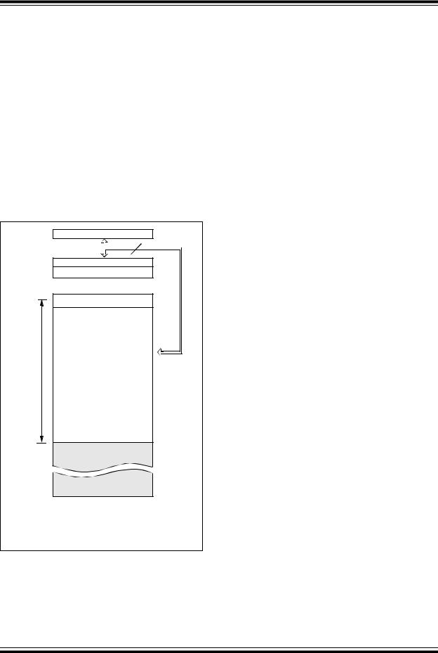
4.2Program Memory Organization for the PIC10F202/206
The PIC10F202/206 devices have a 10-bit Program Counter (PC) capable of addressing a 1024 x 12 program memory space.
Only the first 512 x 12 (0000h-01FFh) for the PIC10F202/206 are physically implemented (see Figure 4-2). Accessing a location above these boundaries will cause a wraparound within the first 512 x 12 space (PIC10F202/206). The effective Reset vector is at 0000h (see Figure 4-2). Location 01FFh (PIC10F202/206) contains the internal clock oscillator calibration value. This value should never be overwritten.
FIGURE 4-2: PROGRAM MEMORY MAP AND STACK FOR THE PIC10F202/206
PC<8:0>
CALL, RETLW |
|
|
|
10 |
|
|
|||
|
|
|
|
|
Stack Level 1 |
|
Stack Level 2 |
|
Reset Vector(1) |
0000h |
On-chip Program |
|
Memory |
|
User Memory Space |
|
512 Words |
01FFh |
|
0200h |
|
02FFh |
Note 1: Address 0000h becomes the effective Reset vector. Location 01FFh contains the MOVLW XX internal oscillator calibration value.
4.3Data Memory Organization
Data memory is composed of registers or bytes of RAM. Therefore, data memory for a device is specified by its register file. The register file is divided into two functional groups: Special Function Registers (SFR) and General Purpose Registers (GPR).
The Special Function Registers include the TMR0 register, the Program Counter (PCL), the STATUS register, the I/O register (GPIO) and the File Select Register (FSR). In addition, Special Function Registers are used to control the I/O port configuration and prescaler options.
The General Purpose registers are used for data and control information under command of the instructions.
For the PIC10F200/204, the register file is composed of 7 Special Function registers and 16 General Purpose registers (see Figure 4-3 and Figure 4-4).
For the PIC10F202/206, the register file is composed of 8 Special Function registers and 24 General Purpose registers (see Figure 4-4).
4.3.1GENERAL PURPOSE REGISTER FILE
The General Purpose Register file is accessed, either directly or indirectly, through the File Select Register (FSR). See Section 4.9 “Indirect Data Addressing: INDF and FSR Registers”.
DS41239D-page 16 |
♥ 2007 Microchip Technology Inc. |

PIC10F200/202/204/206
FIGURE 4-3: |
|
PIC10F200/204 REGISTER |
|
|
|
FILE MAP |
|
File Address |
|
|
|
|
|
|
|
|
00h |
INDF(1) |
|
|
01h |
TMR0 |
|
|
02h |
PCL |
|
|
03h |
STATUS |
|
|
04h |
FSR |
|
|
05h |
OSCCAL |
|
|
|
|
|
|
06h |
GPIO |
|
|
|
|
|
|
07h |
CMCON0(2) |
|
|
08h |
Unimplemented(3) |
|
|
|
|
|
|
0Fh |
|
|
|
10h |
|
|
|
General |
|
|
|
|
|
|
|
|
Purpose |
|
|
|
Registers |
|
|
1Fh |
|
|
Note 1: |
Not a |
physical register. See Section 4.9 |
|
|
“Indirect Data Addressing: INDF and |
||
|
FSR Registers”. |
||
2: PIC10F204 only. Unimplemented on the |
|||
|
PIC10F200 and reads as 00h. |
||
3: |
Unimplemented, read as 00h. |
||
|
|
|
|
FIGURE 4-4: |
PIC10F202/206 REGISTER |
|
|
FILE MAP |
|
File Address |
|
|
|
|
|
00h |
INDF(1) |
|
01h |
TMR0 |
|
02h |
PCL |
|
03h |
STATUS |
|
04h |
FSR |
|
05h |
OSCCAL |
|
06h |
GPIO |
|
|
|
|
07h |
CMCON0(2) |
|
08h |
|
|
|
General |
|
|
Purpose |
|
|
Registers |
|
1Fh |
|
|
Note 1: Not a physical register. See Section 4.9 |
||
“Indirect Data Addressing: INDF and |
||
FSR Registers”. |
||
2: PIC10F206 only. Unimplemented on the |
||
PIC10F202 and reads as 00h. |
||
|
|
|
♥ 2007 Microchip Technology Inc. |
DS41239D-page 17 |