

UM0470
User manual
STM8 SWIM communication protocol and debug module
Introduction
This manual has been written for developers who need to build programming, testing or debugging tools for the STM8 microcontroller family. It explains the debug architecture of the STM8 core.
The STM8 debug system consists of two modules:
●DM: Debug module
●SWIM: Single wire interface module
Related documentation:
●How to program STM8S and STM8A Flash program memory and data EEPROM (PM0051)
(STM8A version is not published yet)
●How to program STM8L Flash program memory and data EEPROM (PM0054)
June 2011 |
Doc ID 14024 Rev 3 |
1/37 |
www.st.com

Contents |
UM0470 |
|
|
Contents
1 |
Debug system overview . . . . . . . . . . . . . . . . . . . . . . . . . . . . . . . . . . . . . |
. 6 |
|
2 |
Communication layer . . . . . . . . . . . . . . . . . . . . . . . . . . . . . . . . . . . . . . . . |
7 |
|
3 |
Single wire interface module (SWIM) . . . . . . . . . . . . . . . . . . . . . . . . . . . |
8 |
|
|
3.1 |
Operating modes . . . . . . . . . . . . . . . . . . . . . . . . . . . . . . . . . . . . . . . . . . . . |
8 |
|
3.2 |
SWIM entry sequence . . . . . . . . . . . . . . . . . . . . . . . . . . . . . . . . . . . . . . . . |
9 |
|
3.3 |
Bit format . . . . . . . . . . . . . . . . . . . . . . . . . . . . . . . . . . . . . . . . . . . . . . . . . |
11 |
3.3.1 High speed bit format . . . . . . . . . . . . . . . . . . . . . . . . . . . . . . . . . . . . . . . 11 3.3.2 Low speed bit format . . . . . . . . . . . . . . . . . . . . . . . . . . . . . . . . . . . . . . . 12
3.4 SWIM communication protocol . . . . . . . . . . . . . . . . . . . . . . . . . . . . . . . . . 13 3.5 SWIM commands . . . . . . . . . . . . . . . . . . . . . . . . . . . . . . . . . . . . . . . . . . . 14
3.5.1 SRST: system reset . . . . . . . . . . . . . . . . . . . . . . . . . . . . . . . . . . . . . . . . 14 3.5.2 ROTF: read on the fly . . . . . . . . . . . . . . . . . . . . . . . . . . . . . . . . . . . . . . 14 3.5.3 WOTF: write on the fly . . . . . . . . . . . . . . . . . . . . . . . . . . . . . . . . . . . . . . 15
3.6 SWIM communication reset . . . . . . . . . . . . . . . . . . . . . . . . . . . . . . . . . . . 15 3.7 CPU register access . . . . . . . . . . . . . . . . . . . . . . . . . . . . . . . . . . . . . . . . . 16 3.8 SWIM communication in Halt mode . . . . . . . . . . . . . . . . . . . . . . . . . . . . . 16 3.9 Physical layer . . . . . . . . . . . . . . . . . . . . . . . . . . . . . . . . . . . . . . . . . . . . . . 17 3.10 STM8 SWIM registers . . . . . . . . . . . . . . . . . . . . . . . . . . . . . . . . . . . . . . . 18
3.10.1 SWIM control status register (SWIM_CSR) . . . . . . . . . . . . . . . . . . . . . . 18 3.10.2 SWIM clock control register (CLK_SWIMCCR) . . . . . . . . . . . . . . . . . . . 19
4 |
Debug module (DM) . . . . . . . . . . . . . . . . . . . . . . . . . . . . . . . . . . . . . . . . |
20 |
|
|
4.1 |
Introduction . . . . . . . . . . . . . . . . . . . . . . . . . . . . . . . . . . . . . . . . . . . . . . . |
20 |
|
4.2 |
Main features . . . . . . . . . . . . . . . . . . . . . . . . . . . . . . . . . . . . . . . . . . . . . . |
20 |
|
4.3 |
Debug . . . . . . . . . . . . . . . . . . . . . . . . . . . . . . . . . . . . . . . . . . . . . . . . . . . . |
22 |
4.3.1 Reset . . . . . . . . . . . . . . . . . . . . . . . . . . . . . . . . . . . . . . . . . . . . . . . . . . . 22 4.3.2 Breakpoints . . . . . . . . . . . . . . . . . . . . . . . . . . . . . . . . . . . . . . . . . . . . . . 22 4.3.3 Abort . . . . . . . . . . . . . . . . . . . . . . . . . . . . . . . . . . . . . . . . . . . . . . . . . . . 22 4.3.4 Watchdog control . . . . . . . . . . . . . . . . . . . . . . . . . . . . . . . . . . . . . . . . . . 22 4.3.5 Interaction with SWIM . . . . . . . . . . . . . . . . . . . . . . . . . . . . . . . . . . . . . . 22
4.4 Breakpoint decoding table . . . . . . . . . . . . . . . . . . . . . . . . . . . . . . . . . . . . 23
2/37 |
Doc ID 14024 Rev 3 |

UM0470 |
Contents |
|
|
4.5 Software breakpoint mode . . . . . . . . . . . . . . . . . . . . . . . . . . . . . . . . . . . . 24 4.6 Timing description . . . . . . . . . . . . . . . . . . . . . . . . . . . . . . . . . . . . . . . . . . 24 4.7 Abort . . . . . . . . . . . . . . . . . . . . . . . . . . . . . . . . . . . . . . . . . . . . . . . . . . . . . 24 4.8 Data breakpoint . . . . . . . . . . . . . . . . . . . . . . . . . . . . . . . . . . . . . . . . . . . . 25 4.9 Instruction breakpoint . . . . . . . . . . . . . . . . . . . . . . . . . . . . . . . . . . . . . . . . 25 4.10 Step mode . . . . . . . . . . . . . . . . . . . . . . . . . . . . . . . . . . . . . . . . . . . . . . . . 25 4.11 Application notes . . . . . . . . . . . . . . . . . . . . . . . . . . . . . . . . . . . . . . . . . . . 26
4.11.1 Illegal Memory access . . . . . . . . . . . . . . . . . . . . . . . . . . . . . . . . . . . . . . 26 4.11.2 Forbidden stack access . . . . . . . . . . . . . . . . . . . . . . . . . . . . . . . . . . . . . 26 4.11.3 DM break . . . . . . . . . . . . . . . . . . . . . . . . . . . . . . . . . . . . . . . . . . . . . . . . 26
4.12 DM registers . . . . . . . . . . . . . . . . . . . . . . . . . . . . . . . . . . . . . . . . . . . . . . . 27
4.12.1 DM breakpoint register 1 extended byte (DM_BKR1E) . . . . . . . . . . . . . 27 4.12.2 DM breakpoint register 1 high byte (DM_BKR1H) . . . . . . . . . . . . . . . . . 27 4.12.3 DM breakpoint register 1 low byte (DM_BKR1L) . . . . . . . . . . . . . . . . . . 27 4.12.4 DM breakpoint register 2 extended byte (DM_BKR2E) . . . . . . . . . . . . . 28 4.12.5 DM breakpoint register 2 high byte (DM_BKR2H) . . . . . . . . . . . . . . . . . 28 4.12.6 DM breakpoint register 2 low byte (DM_BKR2L) . . . . . . . . . . . . . . . . . . 28 4.12.7 DM control register 1 (DM_CR1) . . . . . . . . . . . . . . . . . . . . . . . . . . . . . . 29 4.12.8 DM control register 2 (DM_CR2) . . . . . . . . . . . . . . . . . . . . . . . . . . . . . . 30 4.12.9 DM control/status register 1 (DM_CSR1) . . . . . . . . . . . . . . . . . . . . . . . 31 4.12.10 DM control/status register 2 (DM_CSR2) . . . . . . . . . . . . . . . . . . . . . . . 32 4.12.11 DM enable function register (DM_ENFCTR) . . . . . . . . . . . . . . . . . . . . . 33 4.12.12 Summary of SWIM, DM and core register maps . . . . . . . . . . . . . . . . . . 34
Appendix A Description of the DM_ENFCTR register
for each STM8 product . . . . . . . . . . . . . . . . . . . . . . . . . . . . . . . . . . . 35
Revision history . . . . . . . . . . . . . . . . . . . . . . . . . . . . . . . . . . . . . . . . . . . . . . . . . . . . 36
Doc ID 14024 Rev 3 |
3/37 |

List of tables |
UM0470 |
|
|
List of tables
Table 1. SWIM command summary . . . . . . . . . . . . . . . . . . . . . . . . . . . . . . . . . . . . . . . . . . . . . . . . . 14 Table 2. CPU register memory mapping in STM8 . . . . . . . . . . . . . . . . . . . . . . . . . . . . . . . . . . . . . . 16 Table 3. SWIM pin characteristics . . . . . . . . . . . . . . . . . . . . . . . . . . . . . . . . . . . . . . . . . . . . . . . . . . 17 Table 4. Decoding table for breakpoint interrupt generation. . . . . . . . . . . . . . . . . . . . . . . . . . . . . . . 23 Table 5. STM8 registers . . . . . . . . . . . . . . . . . . . . . . . . . . . . . . . . . . . . . . . . . . . . . . . . . . . . . . . . . . 34 Table 6. Peripherals which are frozen by the bits of the DM_ENFCTR register
for each STM8 product . . . . . . . . . . . . . . . . . . . . . . . . . . . . . . . . . . . . . . . . . . . . . . . . . . . . 35 Table 7. Document revision history . . . . . . . . . . . . . . . . . . . . . . . . . . . . . . . . . . . . . . . . . . . . . . . . . 36
4/37 |
Doc ID 14024 Rev 3 |

UM0470 |
List of figures |
|
|
List of figures
Figure 1. Debug system block diagram . . . . . . . . . . . . . . . . . . . . . . . . . . . . . . . . . . . . . . . . . . . . . . . . 6 Figure 2. SWIM pin external connections . . . . . . . . . . . . . . . . . . . . . . . . . . . . . . . . . . . . . . . . . . . . . . 7 Figure 3. SWIM activation sequence . . . . . . . . . . . . . . . . . . . . . . . . . . . . . . . . . . . . . . . . . . . . . . . . . . 8 Figure 4. SWIM activation timing diagram . . . . . . . . . . . . . . . . . . . . . . . . . . . . . . . . . . . . . . . . . . . . . . 9 Figure 5. SWIM entry sequence . . . . . . . . . . . . . . . . . . . . . . . . . . . . . . . . . . . . . . . . . . . . . . . . . . . . 10 Figure 6. High speed bit format . . . . . . . . . . . . . . . . . . . . . . . . . . . . . . . . . . . . . . . . . . . . . . . . . . . . . 11 Figure 7. Low speed bit format . . . . . . . . . . . . . . . . . . . . . . . . . . . . . . . . . . . . . . . . . . . . . . . . . . . . . 12 Figure 8. Command format (Host -> Target) . . . . . . . . . . . . . . . . . . . . . . . . . . . . . . . . . . . . . . . . . . . 13 Figure 9. Data format (Target -> Host). . . . . . . . . . . . . . . . . . . . . . . . . . . . . . . . . . . . . . . . . . . . . . . . 13 Figure 10. Timings on SWIM pin . . . . . . . . . . . . . . . . . . . . . . . . . . . . . . . . . . . . . . . . . . . . . . . . . . . . . 17 Figure 11. Debug module block diagram . . . . . . . . . . . . . . . . . . . . . . . . . . . . . . . . . . . . . . . . . . . . . . . 21 Figure 12. STM8 Instruction Model . . . . . . . . . . . . . . . . . . . . . . . . . . . . . . . . . . . . . . . . . . . . . . . . . . . 24 Figure 13. STM8 Debug Module Stall Timing . . . . . . . . . . . . . . . . . . . . . . . . . . . . . . . . . . . . . . . . . . . 24 Figure 14. STM8 DM Data Break Timing. . . . . . . . . . . . . . . . . . . . . . . . . . . . . . . . . . . . . . . . . . . . . . . 25 Figure 15. STM8 DM instruction break timing . . . . . . . . . . . . . . . . . . . . . . . . . . . . . . . . . . . . . . . . . . . 25 Figure 16. STM8 DM step timing . . . . . . . . . . . . . . . . . . . . . . . . . . . . . . . . . . . . . . . . . . . . . . . . . . . . . 25
Doc ID 14024 Rev 3 |
5/37 |
Debug system overview |
UM0470 |
|
|
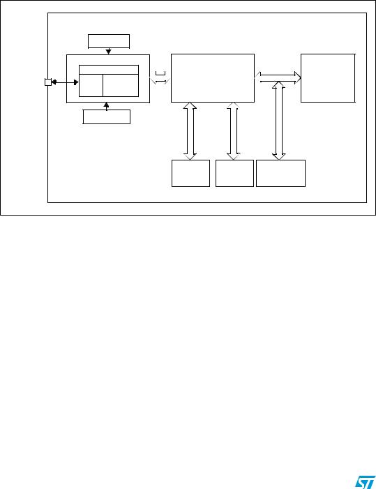
1 Debug system overview
The STM8 debug system interface allows a debugging or programming tool to be connected to the MCU through a single wire bidirectional communication based on open-drain line.
It provides non-intrusive read/write access to RAM and peripherals during program execution
The block diagram is shown in Figure 1.
Figure 1. Debug system block diagram
|
|
STM8 |
|
|
|
|
|
LSI oscillator |
|
|
|
||
|
SWIM |
|
|
|
||
|
SWIM Entry |
|
|
STM8 |
||
SWIM pin |
|
Debug module (DM) |
CPU Bus |
|||
Comm |
Core |
|||||
Command |
|
|
||||
|
Layer |
Decode |
RAMBus |
|
|
|
|
HSI |
PeripheralBus |
|
|
||
|
oscillator |
|
|
|
||
|
|
Peripherals |
RAM |
Flash/ |
|
|
|
|
Data EEPROM |
|
|||
|
|
|
|
|
||
The debug module uses the two internal clock sources present in the device, the LSI Low Speed Internal clock (usually in the range 30 kHz-200 kHz, depending on the product) one and the HSI High Speed Internal clock (usually in the range 10 MHz to 25 MHz, depending on the device). The clocks are automatically started when necessary.
6/37 |
Doc ID 14024 Rev 3 |