

- •1 Central processing unit (CPU)
- •1.1 Introduction
- •1.2 CPU registers
- •1.2.1 Description of CPU registers
- •Figure 2. Stacking order
- •1.2.2 STM8 CPU register map
- •1.3 Global configuration register (CFG_GCR)
- •1.3.1 Activation level
- •1.3.2 SWIM disable
- •1.3.3 Description of global configuration register (CFG_GCR)
- •1.3.4 Global configuration register map and reset values
- •Table 3. CFG_GCR register map
- •2 Boot ROM
- •3 Memory and register map
- •3.1 Memory layout
- •3.1.1 Memory map
- •Figure 3. Memory map
- •3.1.2 Stack handling
- •Figure 4. Default stack model
- •Figure 5. Customized stack model
- •3.2 Register description abbreviations
- •4 Flash program memory and data EEPROM
- •4.1 Introduction
- •4.2 Glossary
- •4.3 Main Flash memory features
- •4.4 Memory organization
- •4.4.1 STM8S and STM8AF memory organization
- •Figure 6. Flash memory and data EEPROM organization on low density STM8S and STM8AF
- •Figure 7. Flash memory and data EEPROM organization on medium density STM8S and STM8AF
- •Figure 8. Flash memory and data EEPROM organization high density STM8S and STM8AF
- •4.4.2 Memory access/ wait state configuration
- •4.4.3 User boot area (UBC)
- •Figure 9. UBC area size definition on low density STM8S devices
- •4.4.4 Data EEPROM (DATA)
- •4.4.5 Main program area
- •4.4.6 Option bytes
- •4.5 Memory protection
- •4.5.1 Readout protection
- •4.5.2 Memory access security system (MASS)
- •4.5.3 Enabling write access to option bytes
- •4.6 Memory programming
- •4.6.2 Byte programming
- •4.6.3 Word programming
- •4.6.4 Block programming
- •4.6.5 Option byte programming
- •4.8 Flash registers
- •4.8.1 Flash control register 1 (FLASH_CR1)
- •4.8.2 Flash control register 2 (FLASH_CR2)
- •4.8.3 Flash complementary control register 2 (FLASH_NCR2)
- •4.8.4 Flash protection register (FLASH_FPR)
- •4.8.5 Flash protection register (FLASH_NFPR)
- •4.8.6 Flash program memory unprotecting key register (FLASH_PUKR)
- •4.8.7 Data EEPROM unprotection key register (FLASH_DUKR)
- •4.8.8 Flash status register (FLASH_IAPSR)
- •4.8.9 Flash register map and reset values
- •5 Single wire interface module (SWIM) and debug module (DM)
- •5.1 Introduction
- •5.2 Main features
- •Figure 12. SWIM pin connection
- •5.3 SWIM modes
- •6 Interrupt controller (ITC)
- •6.1 ITC introduction
- •6.2 Interrupt masking and processing flow
- •Figure 13. Interrupt processing flowchart
- •6.2.1 Servicing pending interrupts
- •Figure 14. Priority decision process
- •6.2.2 Interrupt sources
- •6.3 Interrupts and low power modes
- •6.4 Activation level/low power mode control
- •6.5 Concurrent and nested interrupt management
- •6.5.1 Concurrent interrupt management mode
- •Figure 15. Concurrent interrupt management
- •6.5.2 Nested interrupt management mode
- •Table 10. Vector address map versus software priority bits
- •Figure 16. Nested interrupt management
- •6.6 External interrupts
- •6.7 Interrupt instructions
- •6.8 Interrupt mapping
- •6.9 ITC and EXTI registers
- •6.9.1 CPU condition code register interrupt bits (CCR)
- •6.9.2 Software priority register x (ITC_SPRx)
- •6.9.3 External interrupt control register 1 (EXTI_CR1)
- •6.9.4 External interrupt control register 1 (EXTI_CR2)
- •6.9.5 ITC and EXTI register map and reset values
- •7 Power supply
- •Figure 17. Power supply overview
- •8 Reset (RST)
- •Figure 18. Reset circuit
- •8.1 “Reset state” and “under reset” definitions
- •8.2 Reset circuit description
- •8.3 Internal reset sources
- •Figure 19. VDD/VDDIO voltage detection: POR/BOR threshold
- •8.3.2 Watchdog reset
- •8.3.3 Software reset
- •8.3.4 SWIM reset
- •8.3.5 Illegal opcode reset
- •8.3.6 EMC reset
- •8.4 RST register description
- •8.4.1 Reset status register (RST_SR)
- •8.5 RST register map
- •Table 13. RST register map
- •9 Clock control (CLK)
- •9.1 Master clock sources
- •Figure 21. HSE clock sources
- •Table 14. Devices with 4 trimming bits
- •Table 15. Devices with 3 trimming bits
- •9.2 Master clock switching
- •9.2.1 System startup
- •9.2.2 Master clock switching procedures
- •Figure 22. Clock switching flowchart (automatic mode example)
- •Figure 23. Clock switching flowchart (manual mode example)
- •9.3 Low speed clock selection
- •9.4 CPU clock divider
- •9.5 Peripheral clock gating (PCG)
- •9.6 Clock security system (CSS)
- •9.8 CLK interrupts
- •Table 16. CLK interrupt requests
- •9.9 CLK register description
- •9.9.1 Internal clock register (CLK_ICKR)
- •9.9.2 External clock register (CLK_ECKR)
- •9.9.3 Clock master status register (CLK_CMSR)
- •9.9.4 Clock master switch register (CLK_SWR)
- •9.9.5 Switch control register (CLK_SWCR)
- •9.9.6 Clock divider register (CLK_CKDIVR)
- •9.9.7 Peripheral clock gating register 1 (CLK_PCKENR1)
- •Table 17. Peripheral clock gating bits
- •9.9.8 Peripheral clock gating register 2 (CLK_PCKENR2)
- •Table 18. Peripheral clock gating bits
- •9.9.9 Clock security system register (CLK_CSSR)
- •9.9.10 Configurable clock output register (CLK_CCOR)
- •9.9.11 HSI clock calibration trimming register (CLK_HSITRIMR)
- •9.9.12 SWIM clock control register (CLK_SWIMCCR)
- •9.10 CLK register map and reset values
- •Table 19. CLK register map and reset values
- •10 Power management
- •10.1 General considerations
- •10.1.1 Clock management for low consumption
- •10.2 Low power modes
- •Table 20. Low power mode management
- •10.2.1 Wait mode
- •10.2.2 Halt mode
- •10.3 Additional analog power controls
- •10.3.1 Fast Flash wakeup from Halt mode
- •11 General purpose I/O ports (GPIO)
- •11.1 Introduction
- •11.2 GPIO main features
- •Figure 24. GPIO block diagram
- •11.3 Port configuration and usage
- •11.3.1 Input modes
- •11.3.2 Output modes
- •11.4 Reset configuration
- •11.5 Unused I/O pins
- •11.6 Low power modes
- •Table 22. Effect of low power modes on GPIO ports
- •11.7 Input mode details
- •11.7.1 Alternate function input
- •11.7.2 Interrupt capability
- •11.7.3 Analog channels
- •Table 23. Recommended and non-recommended configurations for analog input
- •11.7.4 Schmitt trigger
- •11.8 Output mode details
- •11.8.1 Alternate function output
- •11.8.2 Slope control
- •11.9 GPIO registers
- •11.9.1 Port x output data register (Px_ODR)
- •11.9.2 Port x pin input register (Px_IDR)
- •11.9.3 Port x data direction register (Px_DDR)
- •11.9.4 Port x control register 1 (Px_CR1)
- •11.9.5 Port x control register 2 (Px_CR2)
- •11.9.6 GPIO register map and reset values
- •12 Auto-wakeup (AWU)
- •12.1 Introduction
- •12.2 LSI clock measurement
- •Figure 25. AWU block diagram
- •12.3 AWU functional description
- •12.3.1 AWU operation
- •12.3.2 Time base selection
- •Table 25. Time base calculation table
- •12.3.3 LSI clock frequency measurement
- •12.4 AWU registers
- •12.4.1 Control/status register (AWU_CSR)
- •12.4.2 Asynchronous prescaler register (AWU_APR)
- •12.4.3 Timebase selection register (AWU_TBR)
- •12.4.4 AWU register map and reset values
- •13 Beeper (BEEP)
- •13.1 Introduction
- •Figure 26. Beep block diagram
- •13.2 Beeper functional description
- •13.2.1 Beeper operation
- •13.2.2 Beeper calibration
- •13.3 Beeper registers
- •13.3.1 Beeper control/status register (BEEP_CSR)
- •13.3.2 Beeper register map and reset values
- •14 Independent watchdog (IWDG)
- •14.1 Introduction
- •14.2 IWDG functional description
- •Figure 27. Independent watchdog (IWDG) block diagram
- •Table 28. Watchdog timeout period (LSI clock frequency = 128 kHz)
- •14.3 IWDG registers
- •14.3.1 Key register (IWDG_KR)
- •14.3.2 Prescaler register (IWDG_PR)
- •14.3.3 Reload register (IWDG_RLR)
- •14.3.4 IWDG register map and reset values
- •15 Window watchdog (WWDG)
- •15.1 Introduction
- •15.2 WWDG main features
- •15.3 WWDG functional description
- •Figure 28. Watchdog block diagram
- •15.4 How to program the watchdog timeout
- •Figure 29. Approximate timeout duration
- •Figure 30. Window watchdog timing diagram
- •Table 30. Window watchdog timing example
- •15.5 WWDG low power modes
- •15.6 Hardware watchdog option
- •15.7 Using Halt mode with the WWDG (WWDGHALT option)
- •15.8 WWDG interrupts
- •15.9 WWDG registers
- •15.9.1 Control register (WWDG_CR)
- •15.9.2 Window register (WWDG_WR)
- •15.10 Window watchdog register map and reset values
- •16 Timer overview
- •Table 33. Timer characteristics
- •16.1 Timer feature comparison
- •16.2 Glossary of timer signal names
- •17 16-bit advanced control timer (TIM1)
- •17.1 Introduction
- •17.2 TIM1 main features
- •Figure 31. TIM1 general block diagram
- •17.3 TIM1 time base unit
- •Figure 32. Time base unit
- •Figure 33. 16-bit read sequence for the counter (TIM1_CNTR)
- •17.3.3 Prescaler
- •Figure 34. Counter in up-counting mode
- •Figure 35. Counter update when ARPE = 0 (ARR not preloaded) with prescaler = 2
- •Figure 36. Counter update event when ARPE = 1 (TIM1_ARR preloaded)
- •Figure 37. Counter in down-counting mode
- •Figure 38. Counter update when ARPE = 0 (ARR not preloaded) with prescaler = 2
- •Figure 39. Counter update when ARPE = 1 (ARR preloaded), with prescaler = 1
- •Figure 40. Counter in center-aligned mode
- •Figure 41. Counter timing diagram, fCK_CNT = fCK_PSC, TIM1_ARR = 06h, ARPE = 1
- •Figure 42. Update rate examples depending on mode and TIM1_RCR register settings
- •17.4 TIM1 clock/trigger controller
- •Figure 43. Clock/trigger controller block diagram
- •17.4.1 Prescaler clock (CK_PSC)
- •Figure 44. Control circuit in normal mode, fCK_PSC = fMASTER
- •17.4.3 External clock source mode 1
- •Figure 45. TI2 external clock connection example
- •Figure 46. Control circuit in external clock mode 1
- •17.4.4 External clock source mode 2
- •Figure 47. External trigger input block diagram
- •Figure 48. Control circuit in external clock mode 2
- •17.4.5 Trigger synchronization
- •Figure 49. Control circuit in trigger mode
- •Figure 50. Control circuit in trigger reset mode
- •Figure 51. Control circuit in trigger gated mode
- •Figure 52. Control circuit in external clock mode 2 + trigger mode
- •17.4.6 Synchronization between TIM1, TIM5 and TIM6 timers
- •Figure 53. Timer chaining system implementation example
- •Figure 54. Trigger/master mode selection blocks
- •Figure 55. Master/slave timer example
- •Figure 56. Gating timer B with OC1REF of timer A
- •Figure 57. Gating timer B with the counter enable signal of timer A (CNT_EN)
- •Figure 58. Triggering timer B with the UEV of timer A (TIMERA-UEV)
- •Figure 59. Triggering timer B with counter enable CNT_EN of timer A
- •Figure 60. Triggering Timer A and B with Timer A TI1 input
- •17.5 TIM1 capture/compare channels
- •Figure 61. Capture/compare channel 1 main circuit
- •Figure 62. 16-bit read sequence for the TIM1_CCRi register in capture mode
- •17.5.2 Input stage
- •Figure 63. Channel input stage block diagram
- •Figure 64. Input stage of TIM 1 channel 1
- •17.5.3 Input capture mode
- •Figure 65. PWM input signal measurement
- •Figure 66. PWM input signal measurement example
- •17.5.4 Output stage
- •Figure 67. Channel output stage block diagram
- •Figure 68. Detailed output stage of channel with complementary output (channel 1)
- •17.5.5 Forced output mode
- •17.5.6 Output compare mode
- •Figure 69. Output compare mode, toggle on OC1
- •17.5.7 PWM mode
- •Figure 70. Edge-aligned counting mode PWM mode 1 waveforms (ARR = 8)
- •Figure 71. Center-aligned PWM waveforms (ARR = 8)
- •Figure 72. Example of one-pulse mode
- •Figure 73. Complementary output with deadtime insertion
- •Figure 74. Deadtime waveforms with a delay greater than the negative pulse
- •Figure 75. Deadtime waveforms with a delay greater than the positive pulse
- •Figure 76. Six-step generation, COM example (OSSR = 1)
- •17.5.8 Using the break function
- •Figure 78. Behavior of outputs in response to a break (TIM1 complementary outputs)
- •17.5.10 Encoder interface mode
- •Table 37. Counting direction versus encoder signals
- •Figure 80. Example of counter operation in encoder interface mode
- •Figure 81. Example of encoder interface mode with IC1 polarity inverted
- •17.6 TIM1 interrupts
- •17.7 TIM1 registers
- •17.7.1 Control register 1 (TIM1_CR1)
- •17.7.2 Control register 2 (TIM1_CR2)
- •17.7.3 Slave mode control register (TIM1_SMCR)
- •17.7.4 External trigger register (TIM1_ETR)
- •17.7.5 Interrupt enable register (TIM1_IER)
- •17.7.6 Status register 1 (TIM1_SR1)
- •17.7.7 Status register 2 (TIM1_SR2)
- •17.7.8 Event generation register (TIM1_EGR)
- •17.7.9 Capture/compare mode register 1 (TIM1_CCMR1)
- •17.7.10 Capture/compare mode register 2 (TIM1_CCMR2)
- •17.7.11 Capture/compare mode register 3 (TIM1_CCMR3)
- •17.7.12 Capture/compare mode register 4 (TIM1_CCMR4)
- •17.7.13 Capture/compare enable register 1 (TIM1_CCER1)
- •17.7.14 Capture/compare enable register 2 (TIM1_CCER2)
- •17.7.15 Counter high (TIM1_CNTRH)
- •17.7.16 Counter low (TIM1_CNTRL)
- •17.7.17 Prescaler high (TIM1_PSCRH)
- •17.7.18 Prescaler low (TIM1_PSCRL)
- •17.7.21 Repetition counter register (TIM1_RCR)
- •17.7.22 Capture/compare register 1 high (TIM1_CCR1H)
- •17.7.23 Capture/compare register 1 low (TIM1_CCR1L)
- •17.7.24 Capture/compare register 2 high (TIM1_CCR2H)
- •17.7.25 Capture/compare register 2 low (TIM1_CCR2L)
- •17.7.26 Capture/compare register 3 high (TIM1_CCR3H)
- •17.7.27 Capture/compare register 3 low (TIM1_CCR3L)
- •17.7.28 Capture/compare register 4 high (TIM1_CCR4H)
- •17.7.29 Capture/compare register 4 low (TIM1_CCR4L)
- •17.7.30 Break register (TIM1_BKR)
- •17.7.31 Deadtime register (TIM1_DTR)
- •17.7.32 Output idle state register (TIM1_OISR)
- •17.7.33 TIM1 register map and reset values
- •18 16-bit general purpose timers (TIM2, TIM3, TIM5)
- •18.1 Introduction
- •18.2 TIM2/TIM3 main features
- •18.3 TIM5 main features
- •18.4 TIM2/TIM3/TIM5 functional description
- •Figure 82. TIM2/TIM3 block diagram
- •Figure 83. TIM5 block diagram
- •18.4.1 Time base unit
- •Figure 84. Time base unit
- •18.4.2 Clock/trigger controller
- •18.4.3 Capture/compare channels
- •Figure 85. Input stage block diagram
- •Figure 86. Input stage of TIM 2 channel 1
- •Figure 87. Output stage
- •Figure 88. Output stage of channel 1
- •18.5 TIM2/TIM3/TIM5 interrupts
- •18.6 TIM2/TIM3/TIM5 registers
- •18.6.1 Control register 1 (TIMx_CR1)
- •18.6.2 Control register 2 (TIM5_CR2)
- •18.6.3 Slave mode control register (TIM5_SMCR)
- •18.6.4 Interrupt enable register (TIMx_IER)
- •18.6.5 Status register 1 (TIMx_SR1)
- •18.6.6 Status register 2 (TIMx_SR2)
- •18.6.7 Event generation register (TIMx_EGR)
- •18.6.8 Capture/compare mode register 1 (TIMx_CCMR1)
- •18.6.9 Capture/compare mode register 2 (TIMx_CCMR2)
- •18.6.10 Capture/compare mode register 3 (TIMx_CCMR3)
- •18.6.11 Capture/compare enable register 1 (TIMx_CCER1)
- •18.6.12 Capture/compare enable register 2 (TIMx_CCER2)
- •18.6.13 Counter high (TIMx_CNTRH)
- •18.6.14 Counter low (TIMx_CNTRL)
- •18.6.15 Prescaler register (TIMx_PSCR)
- •18.6.18 Capture/compare register 1 high (TIMx_CCR1H)
- •18.6.19 Capture/compare register 1 low (TIMx_CCR1L)
- •18.6.20 Capture/compare register 2 high (TIMx_CCR2H)
- •18.6.21 Capture/compare register 2 low (TIMx_CCR2L)
- •18.6.22 Capture/compare register 3 high (TIMx_CCR3H)
- •18.6.23 Capture/compare register 3 low (TIMx_CCR3L)
- •19 8-bit basic timer (TIM4, TIM6)
- •19.1 Introduction
- •Figure 89. TIM4 block diagram
- •Figure 90. TIM6 block diagram
- •19.2 TIM4 main features
- •19.3 TIM6 main features
- •19.4 TIM4/TIM6 interrupts
- •19.5 TIM4/TIM6 clock selection
- •19.6 TIM4/TIM6 registers
- •19.6.1 Control register 1 (TIMx_CR1)
- •19.6.2 Control register 2 (TIM6_CR2)
- •19.6.3 Slave mode control register (TIM6_SMCR)
- •19.6.4 Interrupt enable register (TIMx_IER)
- •19.6.5 Status register 1 (TIMx_SR)
- •19.6.6 Event generation register (TIMx_EGR)
- •19.6.7 Counter (TIMx_CNTR)
- •19.6.8 Prescaler register (TIMx_PSCR)
- •19.6.10 TIM4/TIM6 register map and reset values
- •20 Serial peripheral interface (SPI)
- •20.1 Introduction
- •20.2 SPI main features
- •20.3 SPI functional description
- •20.3.1 General description
- •Figure 91. SPI block diagram
- •Figure 92. Single master/ single slave application
- •Figure 93. Data clock timing diagram
- •20.3.2 Configuring the SPI in slave mode
- •20.3.3 Configuring the SPI master mode
- •20.3.4 Configuring the SPI for simplex communications
- •20.3.5 Data transmission and reception procedures
- •Figure 95. TXE/RXNE/BSY behavior in slave / full duplex mode (BDM = 0, RXONLY = 0). Case of continuous transfers
- •Figure 97. TXE/BSY in slave transmit-only mode (BDM = 0 and RXONLY = 0). Case of continuous transfers
- •Figure 98. RXNE behavior in receive-only mode (BDM = 0 and RXONLY = 1). Case of continuous transfers
- •Figure 99. TXE/BSY behavior when transmitting (BDM = 0 and RXLONY = 0). Case of discontinuous transfers
- •20.3.6 CRC calculation
- •20.3.7 Status flags
- •20.3.8 Disabling the SPI
- •20.3.9 Error flags
- •20.3.10 SPI low power modes
- •20.3.11 SPI interrupts
- •Table 46. SPI interrupt requests
- •20.4 SPI registers
- •20.4.1 SPI control register 1 (SPI_CR1)
- •20.4.2 SPI control register 2 (SPI_CR2)
- •20.4.3 SPI interrupt control register (SPI_ICR)
- •20.4.4 SPI status register (SPI_SR)
- •20.4.5 SPI data register (SPI_DR)
- •20.4.6 SPI CRC polynomial register (SPI_CRCPR)
- •20.4.7 SPI Rx CRC register (SPI_RXCRCR)
- •20.4.8 SPI Tx CRC register (SPI_TXCRCR)
- •20.5 SPI register map and reset values
- •21 Inter-integrated circuit (I2C) interface
- •21.1 Introduction
- •Figure 100. I2C bus protocol
- •Figure 101. I2C block diagram
- •Figure 102. Transfer sequence diagram for slave transmitter
- •Figure 103. Transfer sequence diagram for slave receiver
- •Figure 104. Transfer sequence diagram for master transmitter
- •Figure 105. Method 1: transfer sequence diagram for master receiver
- •Figure 106. Method 2: transfer sequence diagram for master receiver when N >2
- •Figure 107. Method 2: transfer sequence diagram for master receiver when N=2
- •Figure 108. Method 2: transfer sequence diagram for master receiver when N=1
- •21.4.3 Error conditions
- •21.4.4 SDA/SCL line control
- •Table 49. I2C Interrupt requests
- •Figure 109. I2C interrupt mapping diagram
- •21.7.1 Control register 1 (I2C_CR1)
- •21.7.2 Control register 2 (I2C_CR2)
- •21.7.3 Frequency register (I2C_FREQR)
- •21.7.4 Own address register LSB (I2C_OARL)
- •21.7.5 Own address register MSB (I2C_OARH)
- •21.7.6 Data register (I2C_DR)
- •21.7.7 Status register 1 (I2C_SR1)
- •21.7.8 Status register 2 (I2C_SR2)
- •21.7.9 Status register 3 (I2C_SR3)
- •21.7.10 Interrupt register (I2C_ITR)
- •21.7.11 Clock control register low (I2C_CCRL)
- •21.7.12 Clock control register high (I2C_CCRH)
- •21.7.13 TRISE register (I2C_TRISER)
- •22 Universal asynchronous receiver transmitter (UART)
- •22.1 Introduction
- •Table 52. UART configurations
- •22.2 UART main features
- •22.3 UART functional description
- •Figure 110. UART1 block diagram
- •Figure 111. UART2 block diagram
- •Figure 112. UART3 block diagram
- •Figure 113. UART4 block diagram
- •22.3.1 UART character description
- •Figure 114. Word length programming
- •22.3.2 Transmitter
- •Figure 115. Configurable stop bits
- •Figure 116. TC/TXE behavior when transmitting
- •22.3.3 Receiver
- •Figure 117. Start bit detection
- •Figure 118. Data sampling for noise detection
- •Table 53. Noise detection from sampled data
- •22.3.4 High precision baud rate generator
- •Figure 119. How to code UART_DIV in the BRR registers
- •Table 54. Baud rate programming and error calculation
- •22.3.5 Clock deviation tolerance of the UART receiver
- •Table 55. UART receiver tolerance when UART_DIV[3:0] is zero
- •Table 56. UART receiver’s tolerance when UART_DIV[3:0] is different from zero
- •22.3.6 Parity control
- •Figure 120. Mute mode using idle line detection
- •Figure 121. Mute mode using Address mark detection
- •22.3.8 LIN (local interconnection network) mode
- •22.3.9 UART synchronous communication
- •Figure 122. UART example of synchronous transmission
- •Figure 123. UART data clock timing diagram (M=0)
- •Figure 124. UART data clock timing diagram (M=1)
- •Figure 125. RX data setup/hold time
- •22.3.10 Single wire half duplex communication
- •22.3.11 Smartcard
- •Figure 126. ISO 7816-3 asynchronous protocol
- •Figure 127. Parity error detection using 1.5 stop bits
- •22.3.12 IrDA SIR ENDEC block
- •Figure 129. IrDA data modulation (3/16) - normal mode
- •22.4 LIN mode functional description
- •22.4.1 Master mode
- •Figure 130. Break detection in LIN mode (11-bit break length - LBDL bit is set)
- •Figure 131. Break detection in LIN mode vs framing error detection
- •22.4.2 Slave mode with automatic resynchronization disabled
- •Figure 132. LIN identifier field parity bits
- •Figure 133. LIN identifier field parity check
- •Figure 134. LIN header reception time-out
- •22.4.3 Slave mode with automatic resynchronization enabled
- •Figure 135. LIN synch field measurement
- •Figure 136. UARTDIV read / write operations when LDUM = 0
- •Figure 137. UARTDIV read / write operations when LDUM = 1
- •Figure 138. Bit sampling in reception mode
- •22.4.4 LIN mode selection
- •Table 58. LIN mode selection
- •22.5 UART low power modes
- •Table 59. UART interface behavior in low power modes
- •22.6 UART interrupts
- •Table 60. UART interrupt requests
- •Figure 139. UART interrupt mapping diagram
- •22.7 UART registers
- •22.7.1 Status register (UART_SR)
- •22.7.2 Data register (UART_DR)
- •22.7.3 Baud rate register 1 (UART_BRR1)
- •22.7.4 Baud rate register 2 (UART_BRR2)
- •22.7.5 Control register 1 (UART_CR1)
- •22.7.6 Control register 2 (UART_CR2)
- •22.7.7 Control register 3 (UART_CR3)
- •22.7.8 Control register 4 (UART_CR4)
- •22.7.9 Control register 5 (UART_CR5)
- •22.7.10 Control register 6 (UART_CR6)
- •22.7.11 Guard time register (UART_GTR)
- •22.7.12 Prescaler register (UART_PSCR)
- •22.7.13 UART register map and reset values
- •Table 61. UART1 register map
- •23 Controller area network (beCAN)
- •23.1 Introduction
- •23.2 beCAN main features
- •23.3 beCAN general description
- •Figure 140. CAN network topology
- •23.3.1 CAN 2.0B active core
- •23.3.2 Control, status and configuration registers
- •23.3.3 Tx mailboxes
- •23.3.4 Acceptance filters
- •Figure 141. beCAN block diagram
- •Figure 142. beCAN operating modes
- •23.4 Operating modes
- •23.4.1 Initialization mode
- •23.4.2 Normal mode
- •23.4.3 Sleep mode (low power)
- •23.4.4 Time triggered communication mode
- •23.5 Test modes
- •23.5.1 Silent mode
- •Figure 143. beCAN in silent mode
- •23.5.2 Loop back mode
- •Figure 144. beCAN in loop back mode
- •23.5.3 Loop back combined with silent mode
- •Figure 145. beCAN in combined mode
- •23.6 Functional description
- •23.6.1 Transmission handling
- •Figure 146. Transmit mailbox states
- •23.6.2 Reception handling
- •Figure 147. Receive FIFO states
- •23.6.3 Identifier filtering
- •Figure 148. 32-bit filter bank configuration (FSCx bits = 0b11 in CAN_FCRx register)
- •Figure 149. 16-bit filter bank configuration (FSCx bits = 0b10 in CAN_FCRx register)
- •Figure 150. 16/8-bit filter bank configuration (FSCx bits = 0b01 in CAN_FCRx register)
- •Figure 151. 8-bit filter bank configuration (FSCx bits = 0b00 in CAN_FCRx register)
- •Figure 152. Filter banks configured as in the example in Table 65.
- •23.6.4 Message storage
- •Table 66. Transmit mailbox mapping
- •Table 67. Receive mailbox mapping
- •23.6.5 Error management
- •Figure 153. CAN error state diagram
- •23.6.6 Bit timing
- •Figure 154. Bit timing
- •Figure 155. CAN frames
- •23.7 Interrupts
- •Figure 156. Event flags and interrupt generation
- •23.8 Register access protection
- •23.9 Clock system
- •23.10 beCAN low power modes
- •23.11 beCAN registers
- •23.11.1 CAN master control register (CAN_MCR)
- •23.11.2 CAN master status register (CAN_MSR)
- •23.11.3 CAN transmit status register (CAN_TSR)
- •23.11.4 CAN transmit priority register (CAN_TPR)
- •23.11.5 CAN receive FIFO register (CAN_RFR)
- •23.11.6 CAN interrupt enable register (CAN_IER)
- •23.11.7 CAN diagnostic register (CAN_DGR)
- •23.11.8 CAN page select register (CAN_PSR)
- •23.11.9 CAN error status register (CAN_ESR)
- •23.11.10 CAN error interrupt enable register (CAN_EIER)
- •23.11.11 CAN transmit error counter register (CAN_TECR)
- •23.11.12 CAN receive error counter register (CAN_RECR)
- •23.11.13 CAN bit timing register 1 (CAN_BTR1)
- •23.11.14 CAN bit timing register 2 (CAN_BTR2)
- •23.11.15 Mailbox registers
- •23.11.16 CAN filter registers
- •23.12 CAN register map
- •Figure 157. CAN register mapping
- •23.12.1 Page mapping for CAN
- •Figure 158. CAN page mapping
- •Table 69. beCAN control and status page - register map and reset values
- •24 Analog/digital converter (ADC)
- •24.1 Introduction
- •24.2 ADC main features
- •24.3 ADC extended features
- •Figure 159. ADC1 block diagram
- •24.4 ADC pins
- •24.5 ADC functional description
- •24.5.2 ADC clock
- •24.5.3 Channel selection
- •24.5.4 Conversion modes
- •24.5.5 Overrun flag
- •24.5.6 Analog watchdog
- •Figure 161. Analog watchdog guarded area
- •24.5.7 Conversion on external trigger
- •24.5.8 Analog zooming
- •24.5.9 Timing diagram
- •Figure 162. Timing diagram in single mode (CONT = 0)
- •Figure 163. Timing diagram in continuous mode (CONT = 1)
- •24.6 ADC low power modes
- •Table 73. Low power modes
- •24.7 ADC interrupts
- •Table 74. ADC Interrupts in single and non-buffered continuous mode (ADC1 and ADC2)
- •Table 75. ADC interrupts in buffered continuous mode (ADC1)
- •24.8 Data alignment
- •Figure 164. Right alignment of data
- •Figure 165. Left alignment of data
- •24.9 Reading the conversion result
- •24.10 Schmitt trigger disable registers
- •24.11 ADC registers
- •24.11.1 ADC data buffer register x high (ADC_DBxRH) (x=0..7 or 0..9 )
- •24.11.2 ADC data buffer register x low (ADC_DBxRL) (x=or 0..7 or 0..9)
- •24.11.3 ADC control/status register (ADC_CSR)
- •24.11.4 ADC configuration register 1 (ADC_CR1)
- •24.11.5 ADC configuration register 2 (ADC_CR2)
- •24.11.6 ADC configuration register 3 (ADC_CR3)
- •24.11.7 ADC data register high (ADC_DRH)
- •24.11.8 ADC data register low (ADC_DRL)
- •24.11.9 ADC Schmitt trigger disable register high (ADC_TDRH)
- •24.11.10 ADC Schmitt trigger disable register low (ADC_TDRL)
- •24.11.11 ADC high threshold register high (ADC_HTRH)
- •24.11.12 ADC high threshold register low (ADC_HTRL)
- •24.11.13 ADC low threshold register high (ADC_LTRH)
- •24.11.14 ADC low threshold register low (ADC_LTRL)
- •24.11.15 ADC watchdog status register high (ADC_AWSRH)
- •24.11.16 ADC watchdog status register low (ADC_AWSRL)
- •24.11.17 ADC watchdog control register high (ADC_AWCRH)
- •24.11.18 ADC watchdog control register low (ADC_AWCRL)
- •24.12 ADC register map and reset values
- •Table 78. ADC2 register map and reset values
- •25 Revision history
- •Table 79. Document revision history
16-bit advanced control timer (TIM1) |
RM0016 |
|
|
Deadtime insertion is enabled by setting the CCi E and CCi NE bits, and the MOE bit if the break circuit is present. Each channel embeds an 8-bit deadtime generator. It generates two outputs: OCi and OCi N from a reference waveform, OCi REF. If OCi and OCi N are active high:
●The OCi output signal is the same as the reference signal except for the rising edge, which is delayed relative to the reference rising edge.
●The OCi N output signal is the opposite of the reference signal except for the rising edge, which is delayed relative to the reference falling edge.
If the delay is greater than the width of the active output (OCi or OCi N), the corresponding pulse is not generated.
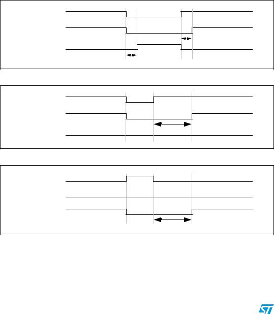
Figure 73, Figure 74, and Figure 75 show the relationships between the output signals of the deadtime generator and the reference signal OCi REF (where CCi P = 0, CCi NP = 0, MOE = 1, CCi E = 1, and CCi NE = 1 in these examples)
Figure 73. Complementary output with deadtime insertion
OCiREF
OCi
delay
OCiN
delay
Figure 74. Deadtime waveforms with a delay greater than the negative pulse
OCiREF
OCi
delay
OCiN
Figure 75. Deadtime waveforms with a delay greater than the positive pulse
OCiREF
OCi
OCiN
delay
The deadtime delay is the same for each of the channels and is programmable with the DTG bits in the TIM1_DTR register. Refer to Section 17.7.31: Deadtime register (TIM1_DTR) on page 212 for delay calculation.
176/454 |
Doc ID 14587 Rev 9 |

RM0016 16-bit advanced control timer (TIM1)
|
Re-directing OCiREF to OCi or OCiN |
|
In output mode (forced, output compare, or PWM), OCiREF can be re-directed to the OCi or |
|
OCiN outputs by configuring the CCiE and CCiNE bits in the corresponding TIM1_CCERi |
|
registers. This means bypassing the deadtime generator which allows a specific waveform |
|
(such as PWM or static active level) to be sent on one output while the complementary |
|
output remains at its inactive level. Alternative possibilities are to have both outputs at |
|
inactive level or both outputs active and complementary with deadtime. |
Note: |
When only OCiN is enabled (CCiE = 0, CCiNE = 1), it is not complemented and becomes |
|
active as soon as OCiREF is high. For example, if CCiNP = 0 then OCiN = OCiREF. On the |
|
other hand, when both OCi and OCiN are enabled (CCiE = CCiNE = 1), OCi becomes active |
|
when OCiREF is high whereas OCiN is complemented and becomes active when OCiREF |
|
is low. |
Six-step PWM generation for motor control
When complementary outputs are implemented on a channel, preload bits are available on the OCi M, CCi E and CCi NE bits. The preload bits are transferred to the active bits at the commutation event (COM). This allows the configuration for the next step to be programmed in advance and for configuration of all the channels to be changed at the same time. The COM event can be generated by software by setting the COMG bit in the TIM1_EGR register or by hardware trigger (on the rising edge of TRGI).
A flag is set when the COM event occurs (COMIF bit in the TIM1_SR register) which can generate an interrupt (if the COMIE bit is set in the TIM1_IER register).
Figure 76 shows the behavior of the OCi and OCi N outputs when a COM event occurs, for three different examples of programmed configurations.
Doc ID 14587 Rev 9 |
177/454 |