

RM0016 |
16-bit advanced control timer (TIM1) |
|
|
17.5.7PWM mode
Pulse width modulation mode allows you to generate a signal with a frequency determined by the value of the TIM1_ARR register and a duty cycle determined by the value of the TIM1_CCRi registers.
The PWM mode can be selected independently on each channel (one PWM per OCi output) by writing 110 (PWM mode 1) or 111 (PWM mode 2) in the OCiM bits in the TIM1_CCMRi registers. The corresponding preload register must be enabled by setting the OCiPE bits in the TIM1_CCMRi registers. The auto-reload preload register (in up-counting or centeraligned modes) may be optionally enabled by setting the ARPE bit in the TIM1_CR1 register.
As the preload registers are transferred to the shadow registers only when an UEV occurs, all registers have to be initialized by setting the UG bit in the TIM1_EGR register before starting the counter.
OCi polarity is software programmable using the CCiP bits in the TIM1_CCERi registers. It can be programmed as active high or active low. The OCi output is enabled by a combination of CCiE, MOE, OISi, OSSR and OSSI bits (TIM1_CCERi and TIM1_BKR registers). Refer to the TIM1_CCERi register descriptions for more details.
In PWM mode (1 or 2), TIM1_CNT and TIM1_CCRi are always compared to determine whether TIM1_CCRi ≤ TIM1_CNT or TIM1_CNT≤ TIM1_CCRi (depending on the direction of the counter).
The timer is able to generate PWM in edge-aligned mode or center-aligned mode depending on the CMS bits in the TIM1_CR1 register.
PWM edge-aligned mode
Up-counting configuration
Up-counting is active when the DIR bit in the TIM1_CR1 register is low.
Example
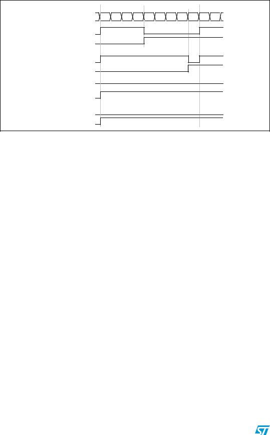
This example uses PWM mode 1. The reference PWM signal, OCiREF, is high as long as TIM1_CNT < TIM1_CCRi. Otherwise, it becomes low. If the compare value in TIM1_CCRi is greater than the auto-reload value (in TIM1_ARR) then OCiREF is held at 1. If the compare value is 0, OCiREF is held at 0. Figure 70 shows some edge-aligned PWM waveforms in an example where TIM1_ARR = 8.
Doc ID 14587 Rev 9 |
171/454 |
16-bit advanced control timer (TIM1) |
RM0016 |
|
|
Figure 70. Edge-aligned counting mode PWM mode 1 waveforms (ARR = 8) |
|
COUNTER REGISTER |
0 |
1 |
2 |
3 |
4 |
5 |
6 |
7 |
8 |
0 |
1 |
OCiREF |
|
|
|
|
|
|
|
|
|
|
|
CCRx = 4 |
|
|
|
|
|
|
|
|
|
|
|
CCiIF |
|
|
|
|
|
|
|
|
|
|
|
OCiREF |
|
|
|
|
|
|
|
|
|
|
|
CCRx = 8 |
|
|
|
|
|
|
|
|
|
|
|
CCiIF |
|
|
|
|
|
|
|
|
|
|
|
OCiREF |
‘1’ |
|
|
|
|
|
|
|
|
|
|
CCRx > 8 |
|
|
|
|
|
|
|
|
|
|
|
CCiIF |
|
|
|
|
|
|
|
|
|
|
|
OCiREF |
‘0’ |
|
|
|
|
|
|
|
|
|
|
CCRx = 0 |
|
|
|
|
|
|
|
|
|
|
|
CCiIF |
|
|
|
|
|
|
|
|
|
|
|
Down-counting configuration
Down-counting is active when the DIR bit in the TIM1_CR1 register is high. Refer to Downcounting mode on page 143
In PWM mode 1, the reference signal OCiREF is low as long as TIM1_CNT> TIM1_CCRi. Otherwise, it becomes high. If the compare value in the TIM1_CCRi registers is greater than the auto-reload value in the TIM1_ARR register, OCiREF is held at 1. Zero percent PWM is not possible in this mode.
PWM center-aligned mode
Center-aligned mode is active when the CMS bits in the TIM1_CR1 register are different from 00 (all the remaining configurations have the same effect on the OCiREF/OCi signals).
The compare flag is set when the counter counts up, down, or up and down depending on the CMS bits configuration. The direction bit (DIR) in the TIM1_CR1 register is updated by hardware and is read-only in this mode (refer to Center-aligned mode (up/down counting) on page 145).
Figure 71 shows some center-aligned PWM waveforms in an example where:
●TIM1_ARR = 8,
●PWM mode is PWM mode 1
●The flag is set (arrow symbol in Figure 71) in three different cases:
–When the counter counts down (CMS = 01)
–When the counter counts up (CMS = 10)
–When the counter counts up and down (CMS = 11)
172/454 |
Doc ID 14587 Rev 9 |

RM0016 |
16-bit advanced control timer (TIM1) |
|
|
Figure 71. Center-aligned PWM waveforms (ARR = 8)
COUNTER REGISTER |
0 |
1 |
2 |
3 |
4 |
5 |
6 |
7 |
8 |
7 |
6 |
5 |
4 |
3 |
2 |
1 |
0 |
1 |
|
|
OCiREF |
|
|
|
|
|
|
|
|
|
|
|
|
|
|
|
|
|
|
CCRx=4 |
CCiIF |
CMS=01 |
|
|
|
|
|
|
|
|
|
|
|
|
|
|
|
|
|
|
|
|
|
|
|
|
|
|
|
|
|
|
|
|
|
|
|
||
|
CMS=10 |
|
|
|
|
|
|
|
|
|
|
|
|
|
|
|
|
||
|
|
|
|
|
|
|
|
|
|
|
|
|
|
|
|
|
|
||
|
|
CMS=11 |
|
|
|
|
|
|
|
|
|
|
|
|
|
|
|
|
|
CCRx=7 |
OCiREF |
|
|
|
|
|
|
|
|
|
|
|
|
|
|
|
|
|
|
CCiIF |
CMS=10 or 11 |
|
|
|
|
|
|
|
|
|
|
|
|
|
|
|
|||
|
|
|
|
|
|
|
|
|
|
|
|
|
|
|
|
||||
CCRx=8 |
OCiREF |
‘1’ |
|
|
|
|
|
|
|
|
|
|
|
|
|
|
|
|
|
|
|
CMS=01 |
|
|
|
|
|
|
|
|
|
|
|
|
|
|
|
|
|
|
CCiIF |
CMS=10 |
|
|
|
|
|
|
|
|
|
|
|
|
|
|
|
|
|
|
|
CMS=11 |
|
|
|
|
|
|
|
|
|
|
|
|
|
|
|
|
|
CCRx>8 |
OCiREF |
‘1’ |
|
|
|
|
|
|
|
|
|
|
|
|
|
|
|
|
|
|
|
CMS=01 |
|
|
|
|
|
|
|
|
|
|
|
|
|
|
|
|
|
|
CCiIF |
CMS=10 |
|
|
|
|
|
|
|
|
|
|
|
|
|
|
|
|
|
|
|
CMS=11 |
|
|
|
|
|
|
|
|
|
|
|
|
|
|
|
|
|
CCRx=0 |
OCiREF |
‘0’ |
|
|
|
|
|
|
|
|
|
|
|
|
|
|
|
|
|
|
|
|
|
|
|
|
|
|
|
|
|
|
|
|
|
|
|
|
|
|
|
|
CMS=01 |
|
|
|
|
|
|
|
|
|
|
|
|
|
|
|
|
|
CCiIF |
|
CMS=10 |
|
|
|
|
|
|
|
|
|
|
|
|
|
|
|
|
|
|
|
CMS=11 |
|
|
|
|
|
|
|
|
|
|
|
|
|
|
|
|
Doc ID 14587 Rev 9 |
173/454 |
16-bit advanced control timer (TIM1) |
RM0016 |
|
|
One-pulse mode
One-pulse mode (OPM) is a particular case of the previous modes. It allows the counter to be started in response to a stimulus and to generate a pulse with a programmable length after a programmable delay.
Starting the counter can be controlled through the clock/trigger controller. Generating the waveform can be done in output compare mode or PWM mode. Select one-pulse mode by setting the OPM bit in the TIM1_CR1 register. This makes the counter stop automatically at the next UEV.
A pulse can be correctly generated only if the compare value is different from the counter initial value. Before starting (when the timer is waiting for the trigger), the configuration must be:
●In up-counting: CNT< CCRi ≤ ARR (in particular, 0 < CCRi),
●In down-counting: CNT> CCRi
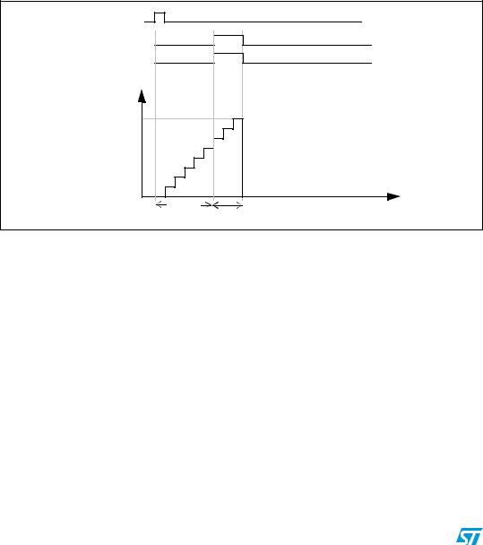
Figure 72. Example of one-pulse mode
|
TI2 |
|
|
OC1REF |
|
|
OC1 |
|
COUNTER |
TIMx_ARR |
|
TIMx_CCR1 |
|
|
|
|
|
|
0 |
|
|
tDELAY |
t |
|
|
tPULSE |
Example
This example shows how to generate a positive pulse on OC1 with a length of tPULSE and after a delay of tDELAY as soon as a positive edge is detected on the TI2 input pin.
Follow the procedure below to use IC2 as trigger 1:
●Map IC2 on TI2 by writing CC2S = 01 in the TIM1_CCMR2 register
●IC2 must detect a rising edge, so write CC2P = 0 in the TIM1_CCER1 register
●Configure IC2 as trigger for the clock/trigger controller (TRGI) by writing TS = 110 in the TIM1_SMCR register.
●IC2 is used to start the counter by writing SMS to 110 in the TIM1_SMCR register (trigger mode).
174/454 |
Doc ID 14587 Rev 9 |

RM0016 |
16-bit advanced control timer (TIM1) |
|
|
The OPM waveform is defined by writing the compare registers (taking into account the clock frequency and the counter prescaler) as follows:
●The tDELAY is defined by the value written in the TIM1_CCR1 register
●The tPULSE is defined by the difference between the auto-reload value and the compare value (TIM1_ARR - TIM1_CCR1).
●To build a waveform with a transition from 0 to 1 when a compare match occurs and a transition from 1 to 0 when the counter reaches the auto-reload value, enable PWM mode 2 by writing OCiM = 111 in the TIM1_CCMR1 register. Alternatively, enable the preload registers by writing OC1PE = 1 in the TIM1_CCMR1 register and ARPE = 0 in the TIM1_CR1 register (optional). In this case, write the compare value in the TIM1_CCR1 register and write the auto-reload value in the TIM1_ARR register. Then, generate an update by setting the UG bit and wait for an external trigger event on TI2. CC1P is written to 0 in this example.
In the example outlined above, the DIR and CMS bits in the TIM1_CR1 register should be low.
As only one pulse is required, write 1 in the OPM bit in the TIM1_CR1 register to stop the counter at the next UEV (when the counter rolls over from the auto-reload value back to 0).
Particular case: OCi fast enable
In one-pulse mode, the edge detection on the TIi input sets the CEN bit which enables the counter. Then, a comparison between the counter and the compare value makes the output toggle. However, several clock cycles are needed for these operations and this affects the the minimum delay (tDELAY min) that can be obtained.
To output a waveform with the minimum delay, set the OCiFE bits in the TIM1_CCMRi registers. OCiREF (and OCi) are forced in response to the stimulus, without taking the comparison into account. The new level of OCiREF (and OCi) is the same as if a compare match had occured. The OCiFE bits acts only if the channel is configured in PWM1 or PWM2 mode.
Complementary outputs and deadtime insertion
TIM1 can output two complementary signals per channel. It also manages the switching-off and switching-on instants of the outputs (see Figure 31: TIM1 general block diagram on page 138).
This time is generally known as deadtime. Deadtimes must be adjusted depending on the characteristics of the devices connected to the outputs (example, intrinsic delays of levelshifters, delays due to power switches).
The polarity of the outputs can be selected (main output OCi or complementary OCi N) independently for each output. This is done by writing to the CCi P and CCi NP bits in the TIM1_CCERi registers.
The complementary signals OCi and OCi N are activated by a combination of several control bits: The CCi E and CCi NE bits in the TIM1_CCERi register and, if the break feature is implemented, the MOE, OISi, OISi N, OSSI, and OSSR bits in the TIM1_BKR register. Refer to Table 38: Output control for complementary OCi and OCiN channels with break feature on page 202 for more details. In particular, the deadtime is activated when switching to the IDLE state (when MOE falls to 0).
Doc ID 14587 Rev 9 |
175/454 |