


Hardware and layout |
UM0817 |
|
|
2.1STM8S105C6T6 microcontroller
Figure 4. STM8S105C6T6 package
The STM8S105C6T6 8-bit microcontroller offers:
32 Kbytes of Flash program memory
1 Kbyte true data EEPROM
2 Kbytes RAM
This device provides the following benefits:
●Reduced system cost
–Integrated true data EEPROM for up to 300 K write/erase cycles
–High system integration level; internal clock oscillators, brown-out reset, watchdog.
●Performance and robustness
–16 MHz CPU clock frequency
–Up to 38 I/Os on a 48-pin package including 16 high sink outputs
–Robust I/O immune against current injection
–Independent watchdogs with separate clock source
–Flexible clock control, 4 master clocks (HSI, LSI, HSE and external HSE)
–Clock security system
–A family of products for applications with 2.95 V to 5.5 V operating supply
●Short development cycles
–Applications scalability across common family product architecture with compatible pinout, memory map and modular peripherals.
–Full documentation and a wide choice of development tools
–Standard S/W library for firmware and touch sensing development quick start
–Numerous application notes and firmware examples available
●Product longevity
–Advanced core and peripherals made in state-of-the-art technology
–Low power modes (wait, active-halt, halt)
–Auto wake-up timer for active halt
–Permanently active, low consumption
●Other features
–Nested interrupt controller with 32 interrupts
–Up to 37 external interrupts on 6 vectors
–2 x 16-bit general purpose timers; with 2+3 CAPCOM channels (IC, OC or PWM)
–Advanced control timer: 16-bit, 4 CAPCOM channels, 3 complementary outputs, deadtime insertion and flexible synchronization
–8-bit basic timer with 8-bit prescaler
–UART with clock output for synchronous operation, Smartcard, IrDA, LIN
–SPI interface up to 8 Mbit/s
–I2C interface up to 400 Kbit/s
–Analog-to-digital converter 10-bit, ±1 LSB ADC with up to 10 multiplexed channels
6/18 |
Doc ID 16361 Rev 3 |
UM0817 |
Hardware and layout |
|
|
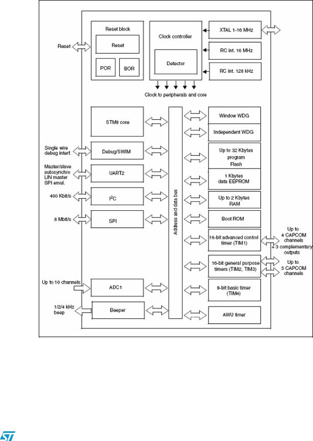
Figure 5. STM8S105 block diagram
For more information see the STM8S105xx datasheet (Doc ID 14771) on the ST website.
Doc ID 16361 Rev 3 |
7/18 |