

- •Features
- •Disclaimer
- •Overview
- •Block Diagram
- •Pin Descriptions
- •Port A (PA7..PA0)
- •Port B (PB7..PB0)
- •Port C (PC7..PC0)
- •Port D (PD7..PD0)
- •RESET
- •XTAL1
- •XTAL2
- •AVCC
- •AREF
- •Resources
- •Data Retention
- •AVR CPU Core
- •Introduction
- •Status Register
- •Stack Pointer
- •I/O Memory
- •Clock Systems and their Distribution
- •Clock Sources
- •Crystal Oscillator
- •External Clock
- •Idle Mode
- •Power-down Mode
- •Power-save Mode
- •Standby Mode
- •Analog Comparator
- •Brown-out Detector
- •Watchdog Timer
- •Port Pins
- •Resetting the AVR
- •Reset Sources
- •Power-on Reset
- •External Reset
- •Watchdog Reset
- •Watchdog Timer
- •Interrupts
- •I/O Ports
- •Introduction
- •Configuring the Pin
- •Reading the Pin Value
- •Unconnected pins
- •Alternate Port Functions
- •Register Description for I/O Ports
- •8-bit Timer/Counter0 with PWM
- •Overview
- •Registers
- •Definitions
- •Counter Unit
- •Normal Mode
- •Fast PWM Mode
- •8-bit Timer/Counter Register Description
- •Timer/Counter0 and Timer/Counter1 Prescalers
- •Internal Clock Source
- •Prescaler Reset
- •External Clock Source
- •16-bit Timer/Counter1
- •Overview
- •Registers
- •Definitions
- •Compatibility
- •Counter Unit
- •Input Capture Unit
- •Noise Canceler
- •Force Output Compare
- •Normal Mode
- •Fast PWM Mode
- •16-bit Timer/Counter Register Description
- •8-bit Timer/Counter2 with PWM and Asynchronous Operation
- •Overview
- •Registers
- •Definitions
- •Counter Unit
- •Normal Mode
- •Fast PWM Mode
- •8-bit Timer/Counter Register Description
- •Slave Mode
- •Master Mode
- •Data Modes
- •USART
- •Overview
- •Clock Generation
- •External Clock
- •Frame Formats
- •Parity Bit Calculation
- •Parity Generator
- •Receiver Error Flags
- •Parity Checker
- •Disabling the Receiver
- •Using MPCM
- •Write Access
- •Read Access
- •Features
- •TWI Terminology
- •Transferring Bits
- •Address Packet Format
- •Data Packet Format
- •Overview of the TWI Module
- •SCL and SDA Pins
- •Bus Interface Unit
- •Address Match Unit
- •Control Unit
- •Using the TWI
- •Master Receiver Mode
- •Slave Receiver Mode
- •Miscellaneous States
- •Analog Comparator Multiplexed Input
- •Analog to Digital Converter
- •Features
- •Operation
- •Changing Channel or Reference Selection
- •ADC Input Channels
- •Analog Input Circuitry
- •Features
- •Overview
- •TAP Controller
- •PRIVATE0; $8
- •PRIVATE1; $9
- •PRIVATE2; $A
- •PRIVATE3; $B
- •Bibliography
- •IEEE 1149.1 (JTAG) Boundary-scan
- •Features
- •System Overview
- •Data Registers
- •Bypass Register
- •Reset Register
- •EXTEST; $0
- •IDCODE; $1
- •AVR_RESET; $C
- •BYPASS; $F
- •Scanning the ADC
- •ATmega16 Boundary-scan Order
- •Features
- •Application Section
- •Read-While-Write and no Read- While-Write Flash Sections
- •Prevent Reading the RWW Section during Self-Programming
- •Simple Assembly Code Example for a Boot Loader
- •Fuse Bits
- •Latching of Fuses
- •Signature Bytes
- •Calibration Byte
- •Page Size
- •Signal Names
- •Chip Erase
- •Reading the Flash
- •Reading the EEPROM
- •Data Polling Flash
- •Data Polling EEPROM
- •AVR_RESET ($C)
- •PROG_ENABLE ($4)
- •Data Registers
- •Reset Register
- •Programming Enable Register
- •Programming Command Register
- •Virtual Flash Page Read Register
- •Performing Chip Erase
- •Reading the Flash
- •Reading the EEPROM
- •Electrical Characteristics
- •Absolute Maximum Ratings*
- •DC Characteristics
- •External Clock Drive Waveforms
- •External Clock Drive
- •Two-wire Serial Interface Characteristics
- •ADC Characteristics
- •Idle Supply Current
- •Pin Pullup
- •Pin Driver Strength
- •Register Summary
- •Instruction Set Summary
- •Ordering Information
- •Packaging Information
- •Errata
 ATmega16(L)
|
6. |
Set OE to “1”. |
||||||
Reading the EEPROM |
The algorithm for reading the EEPROM memory is as follows (refer to “Programming the Flash” |
|||||||
|
on page 265 for details on Command and Address loading): |
|||||||
|
1. |
A: Load Command “0000 0011”. |
||||||
|
2. |
G: Load Address High Byte ($00 - $FF) |
||||||
|
3. |
B: Load Address Low Byte ($00 - $FF) |
||||||
|
4. |
Set |
|
|
to “0”, and BS1 to “0”. The EEPROM Data byte can now be read at DATA. |
|||
|
OE |
|||||||
|
5. |
Set |
|
|
to “1”. |
|||
|
OE |
|||||||
Programming the |
The algorithm for programming the Fuse Low bits is as follows (refer to “Programming the Flash” |
|||||||
Fuse Low Bits |
on page 265 for details on Command and Data loading): |
|||||||
|
1. |
A: Load Command “0100 0000”. |
||||||
|
2. |
C: Load Data Low Byte. Bit n = “0” programs and bit n = “1” erases the Fuse bit. |
||||||
|
3. |
Set BS1 to “0” and BS2 to “0”. |
||||||
|
4. |
Give |
|
|
|
to go high. |
||
|
WR |
a negative pulse and wait for RDY/BSY |
||||||
Programming the |
The algorithm for programming the Fuse high bits is as follows (refer to “Programming the Flash” |
|||||||
Fuse High Bits |
on page 265 for details on Command and Data loading): |
|||||||
|
1. |
A: Load Command “0100 0000”. |
||||||
|
2. |
C: Load Data Low Byte. Bit n = “0” programs and bit n = “1” erases the Fuse bit. |
||||||
|
3. |
Set BS1 to “1” and BS2 to “0”. This selects high data byte. |
||||||
|
4. |
Give |
|
|
|
to go high. |
||
|
WR |
a negative pulse and wait for RDY/BSY |
||||||
|
5. |
Set BS1 to “0”. This selects low data byte. |
||||||
Figure 131. Programming the Fuses
|
|
|
Write Fuse Low byte |
|
|
Write Fuse high byte |
|
A |
C |
|
A |
C |
|
DATA |
$40 |
DATA |
XX |
$40 |
DATA |
XX |
|
|
|
|
|
|
XA1
XA0
BS1
BS2
XTAL1
WR
RDY/BSY
RESET +12V
OE
PAGEL
269
2466P–AVR–08/07
Programming the Lock The algorithm for programming the Lock bits is as follows (refer to “Programming the Flash” on Bits page 265 for details on Command and Data loading):
1.A: Load Command “0010 0000”.
2.C: Load Data Low Byte. Bit n = “0” programs the Lock bit.
3.Give WR a negative pulse and wait for RDY/BSY to go high.
The Lock bits can only be cleared by executing Chip Erase.
Reading the Fuse and The algorithm for reading the Fuse and Lock bits is as follows (refer to “Programming the Flash” Lock Bits on page 265 for details on Command loading):
1.A: Load Command “0000 0100”.
2.Set OE to “0”, BS2 to “0” and BS1 to “0”. The status of the Fuse Low bits can now be read at DATA (“0” means programmed).
3.Set OE to “0”, BS2 to “1” and BS1 to “1”. The status of the Fuse High bits can now be read at DATA (“0” means programmed).
4.Set OE to “0”, BS2 to “0” and BS1 to “1”. The status of the Lock bits can now be read at DATA (“0” means programmed).
5.Set OE to “1”.
Figure 132. Mapping between BS1, BS2 and the Fuseand Lock Bits during Read
|
|
|
|
|
Fuse Low Byte |
|
|
0 |
DATA |
||||||||
|
|
|
|
|
|
|
|||||||||||
|
|
|
|
|
|
|
|
|
|
|
|
|
|
|
|
||
|
|
|
|
|
Lock Bits |
|
|
0 |
|
|
|
|
1 |
|
|
||
|
|
|
|
|
|
|
|
|
|
|
|
|
|||||
|
|
|
|
|
|
|
|
|
|
|
|
|
|||||
|
|
|
|
|
|
|
|
|
|
|
|
|
|||||
|
|
|
|
|
|
|
|
|
|
|
|
|
|||||
|
|
|
|
|
|
|
|
|
|
|
|
|
|
|
|
|
|
|
|
|
|
|
|
|
|
|
|
|
BS1 |
|
|
|
|||
|
|
|
|
|
Fuse High Byte |
|
1 |
||||||||||
|
|
|
|
|
|
|
|
|
|
|
|
|
|
||||
|
|
|
|
|
|
|
|
|
|
|
|
|
|
||||
|
|
|
|
|
|
|
|
|
|
|
|
|
|
|
|
|
|
Reading the Signature |
|
|
|
|
BS2 |
|
|
|
|
|
|
|
|
|
|
|
|
|
|
|
|
|
|
|
|
|
|
|
|
|
|
|
|
||
|
|
|
|
|
|
|
|
|
|
|
|
|
|
|
|
||
The algorithm for reading the Signature bytes is as follows (refer to “Programming the Flash” on |
|||||||||||||||||
Bytes |
page 265 for details on Command and Address loading): |
||||||||||||||||
|
1. |
A: Load Command “0000 1000”. |
|
|
|
|
|
|
|
|
|
|
|
||||
|
2. |
B: Load Address Low Byte ($00 - $02). |
|||||||||||||||
|
3. |
Set |
|
to “0”, and BS1 to “0”. The selected Signature byte can now be read at DATA. |
|||||||||||||
|
OE |
||||||||||||||||
|
4. |
Set |
|
to “1”. |
|
|
|
|
|
|
|
|
|
|
|
||
|
OE |
|
|
|
|
|
|
|
|
|
|
|
|||||
Reading the |
The algorithm for reading the Calibration byte is as follows (refer to “Programming the Flash” on |
||||||||||||||||
Calibration Byte |
page 265 for details on Command and Address loading): |
||||||||||||||||
|
1. |
A: Load Command “0000 1000”. |
|
|
|
|
|
|
|
|
|
|
|
||||
|
2. |
B: Load Address Low Byte, $00. |
|
|
|
|
|
|
|
|
|
|
|
||||
|
3. |
Set |
|
to “0”, and BS1 to “1”. The Calibration byte can now be read at DATA. |
|||||||||||||
|
OE |
||||||||||||||||
|
4. |
Set |
|
to “1”. |
|
|
|
|
|
|
|
|
|
|
|
||
|
OE |
|
|
|
|
|
|
|
|
|
|
|
|||||
270 ATmega16(L) 
2466P–AVR–08/07
 ATmega16(L)
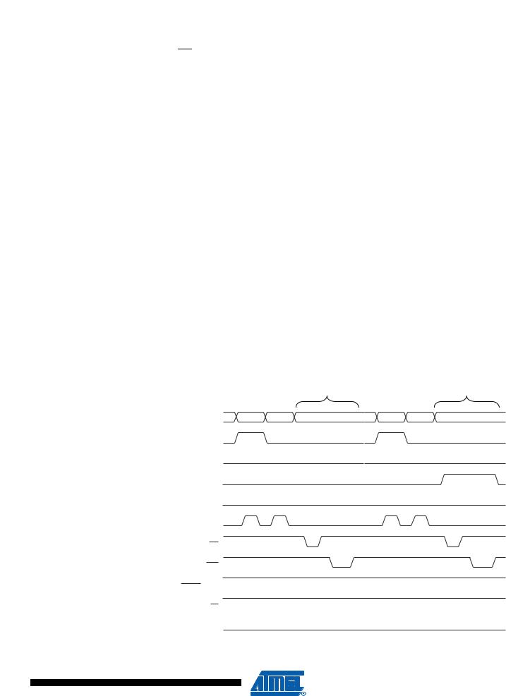
Parallel Programming Figure 133. Parallel Programming Timing, Including some General Timing Requirements |
||||||||||||||||||||||||||||||||||||||||
Characteristics |
|
|
|
|
|
|
|
|
|
|
|
|
|
|
|
tXLWL |
|
|
|
|
|
|
|
|
|
|
|
|
|
|
|
|
|
|
|
|
|
|
|
|
|
|
|
|
|
|
|
|
|
|
|
|
|
|
|
|
|
|
|
|
|
|
|
|
|
|
|
|
|
|
|
|
|
|
|
|
|
|
|
||
|
|
XTAL1 |
|
|
|
tXHXL |
|
|
|
|
|
|
|
|
|
|
|
|
|
|
|
|
|
|
|
|
|
|
|
|
|
|
||||||||
|
|
Data & Contol |
|
tDVXH |
|
|
|
|
|
|
|
|
tXLDX |
|
|
|
|
|
|
|
|
|
|
|
|
|
|
|
|
|
|
|
|
|
|
|
||||
|
|
|
|
|
|
|
|
|
|
|
|
|
|
|
|
|
|
|
|
|
|
|
|
|
|
|
|
|
|
|
|
|
|
|
|
|
||||
|
|
|
|
|
|
|
|
|
|
|
|
|
|
|
|
|
|
|
|
|
|
|
|
|
|
|
|
|
|
|
|
|
|
|
|
|||||
(DATA, XA0/1, BS1, BS2) |
|
|
|
|
|
|
|
|
|
|
|
|
|
|
|
|
|
|
|
|
|
|
|
|
|
|
|
|
|
|
|
|
|
|
|
|||||
|
|
|
|
|
|
|
tBVPH |
|
|
|
|
|
|
|
|
tPLBX |
|
t BVWL |
|
|
|
|
|
|
|
|
|
|
tWLBX |
|
|
|
||||||||
|
|
|
|
|
|
|
|
|
|
|
|
|
|
|
|
|
|
|
|
|
|
|
|
|
|
|
|
|
|
|
|
|
|
|
|
|
||||
|
|
PAGEL |
|
|
|
tPHPL |
|
|
|
|
|
|
|
|
tWL WH |
|
|
|
|
|
|
|
|
|
|
|
|
|
||||||||||||
|
|
|
|
|
|
|
|
|
|
|
|
|
|
|
|
|
|
|
|
|
|
|
|
|
|
|
|
|
|
|
|
|
|
|
|
|||||
|
|
|
WR |
|
|
|
|
|
|
|
|
tPLWL |
|
|
|
|
|
|
|
|
|
|
|
|
|
|
|
|
|
|
|
|
|
|
|
|||||
|
|
|
|
|
|
|
|
|
|
|
|
|
|
|
|
|
|
|
|
|
WLRL |
|
|
|
|
|
|
|
|
|
||||||||||
|
|
|
|
|
|
|
|
|
|
|
|
|
|
|
|
|
|
|
|
|
|
|
|
|
|
|
|
|
|
|
|
|
||||||||
|
|
|
|
|
|
|
|
|
|
|
|
|
|
|
|
|
|
|
|
|
|
|
|
|
|
|
|
|
|
|
|
|
|
|
|
|
|
|
|
|
|
|
RDY/BSY |
|
|
|
|
|
|
|
|
|
|
|
|
|
|
|
|
|
|
|
|
|
|
|
|
|
|
|
|
|
|
|
|
|
|||||
|
|
|
|
|
|
|
|
|
|
|
|
|
|
|
|
|
|
|
|
|
|
|
|
|
|
|
|
|
|
|
|
|
|
|
|
|
|
tWLRH |
||
|
|
|
|
|
|
|
|
|
|
|
|
|
|
|
|
|
|
|
|
|
|
|
|
|
|
|
|
|
|
|
|
|
|
|
|
|
|
|||
Figure 134. Parallel Programming Timing, Loading Sequence with Timing Requirements(1) |
||||||||||||||||||||||||||||||||||||||||
|
|
LOAD ADDRESS |
LOAD DATA |
|
|
LOAD DATA LOAD DATA |
|
|
LOAD ADDRESS |
|||||||||||||||||||||||||||||||
|
|
(LOW BYTE) |
(LOW BYTE) |
|
(HIGH BYTE) |
|
|
|
(LOW BYTE) |
|||||||||||||||||||||||||||||||
|
|
|
|
|
|
|
|
|
|
|
|
|
|
|
|
t XLXH |
|
|
|
|
|
|
tXLPH |
tPLXH |
|
|
|
|
|
|||||||||||
XTAL1 |
|
|
|
|
|
|
|
|
|
|
|
|
|
|
|
|
|
|
|
|
|
|
|
|
|
|
|
|
|
|
|
|
|
|
|
|
|
|
|
|
BS1 |
|
|
|
|
|
|
|
|
|
|
|
|
|
|
|
|
|
|
|
|
|
|
|
|
|
|
|
|
|
|
|
|
|
|
|
|
|
|
|
|
PAGEL |
|
|
|
|
|
|
|
|
|
|
|
|
|
|
|
|
|
|
|
|
|
|
|
|
|
|
|
|
|
|
|
|
|
|
|
|
|
|
|
|
DATA |
|
ADDR0 (Low Byte) |
|
DATA (Low Byte) |
|
|
|
DATA (High Byte) |
|
|
|
|
ADDR1 (Low Byte) |
|||||||||||||||||||||||||||
XA0 |
|
|
|
|
|
|
|
|
|
|
|
|
|
|
|
|
|
|
|
|
|
|
|
|
|
|
|
|
|
|
|
|
|
|
|
|
|
|
|
|
XA1 |
|
|
|
|
|
|
|
|
|
|
|
|
|
|
|
|
|
|
|
|
|
|
|
|
|
|
|
|
|
|
|
|
|
|
|
|
|
|
|
|
Note: 1. |
The timing requirements shown in Figure 133 (i.e., tDVXH, tXHXL, and tXLDX) also apply to load- |
|||||||||||||||||||||||||||||||||||||||
|
ing operation. |
|
|
|
|
|
|
|
|
|
|
|
|
|
|
|
|
|
|
|
|
|
|
|
|
|
|
|
|
|
|
|
|
|
||||||
271
2466P–AVR–08/07

Figure 135. Parallel Programming Timing, Reading Sequence (within the Same Page) with
Timing Requirements(1)
|
|
|
|
|
|
|
LOAD ADDRESS |
READ DATA |
READ DATA |
LOAD ADDRESS |
||||||||||||||||||||||||||||
|
|
|
|
|
|
|
(LOW BYTE) |
(LOW BYTE) |
(HIGH BYTE) |
(LOW BYTE) |
||||||||||||||||||||||||||||
|
|
|
|
|
|
|
|
|
tXLOL |
|
|
|
|
|
|
|
|
|
|
|
|
|
|
|
||||||||||||||
XTAL1 |
|
|
|
|
|
|
|
|
|
|
|
|
|
|
|
|
|
|
|
|
|
|
|
|
|
|
|
|
|
|
|
|
|
|
|
|
||
BS1 |
|
|
|
|
|
|
|
|
|
|
|
|
|
|
|
|
|
|
|
|
|
|
tBVDV |
|
|
|
|
|
|
|
|
|
|
|
||||
|
|
|
|
|
|
|
|
|
|
|
|
|
|
|
|
|
|
|
|
|
|
|
|
|
|
|
|
|
|
|
|
|
|
|
|
|||
|
|
|
|
|
|
|
|
|
|
|
|
|
|
|
|
tOLDV |
|
|
|
|
|
|
|
|
|
|
|
|
|
|
|
|||||||
|
|
|
|
|
|
|
|
|
|
|
|
|
|
|
|
|
|
|
|
|
|
|
|
|
|
|
|
|
|
|
||||||||
|
|
|
|
|
|
|
|
|
|
|
|
|
|
|
|
|
|
|
|
|
|
|
|
|
|
|
|
|
|
|
|
|
|
|
|
|
||
|
OE |
|
|
|
|
|
|
|
|
|
|
|
|
|
|
|
|
|
|
|
|
|
|
|
|
|
|
|
|
|
tOHDZ |
|
|
|
|
|||
|
|
|
|
|
|
|
|
|
|
|
|
|
|
|
|
|
|
|
|
|
|
|
|
|
|
|
|
|
|
|
|
ADDR1 (Low Byte) |
||||||
|
|
|
|
|
|
|
|
|
|
|
|
|
|
|
||||||||||||||||||||||||
DATA |
|
|
|
|
ADDR0 (Low Byte) |
|
DATA (Low Byte) |
|
DATA (High Byte) |
|
||||||||||||||||||||||||||||
XA0 |
|
|
|
|
|
|
|
|
|
|
|
|
|
|
|
|
|
|
|
|
|
|
|
|
|
|
|
|
|
|
|
|
|
|
|
|
||
|
|
|
|
|
|
|
|
|
|
|
|
|
|
|
|
|
|
|
|
|
|
|
|
|
|
|
|
|
|
|
|
|
|
|
|
|||
XA1 |
|
|
|
|
|
|
|
|
|
|
|
|
|
|
|
|
|
|
|
|
|
|
|
|
|
|
|
|
|
|
|
|
|
|
|
|
||
Note: 1. |
The timing requirements shown in Figure 133 (i.e., tDVXH, tXHXL, and tXLDX) also apply to read- |
|||||||||||||||||||||||||||||||||||||
|
|
|
ing operation. |
|
|
|
|
|
|
|
|
|
|
|
|
|
|
|
||||||||||||||||||||
Table 113. |
|
Parallel Programming Characteristics, VCC = 5 V ± 10% |
|
|
|
|
||||||||||||||||||||||||||||||||
Symbol |
|
|
Parameter |
|
|
|
|
|
Min |
Typ |
|
|
Max |
|
Units |
|
||||||||||||||||||||||
|
|
|
|
|
|
|
|
|
|
|
|
|
|
|
|
|
|
|
|
|
|
|
|
|
|
|
|
|||||||||||
VPP |
|
|
Programming Enable Voltage |
|
|
|
|
|
11.5 |
|
|
|
|
|
12.5 |
|
V |
|
||||||||||||||||||||
IPP |
|
|
Programming Enable Current |
|
|
|
|
|
|
|
|
|
|
|
250 |
|
μA |
|
||||||||||||||||||||
tDVXH |
|
|
Data and Control Valid before XTAL1 High |
67 |
|
|
|
|
|
|
|
ns |
|
|||||||||||||||||||||||||
tXLXH |
|
|
XTAL1 Low to XTAL1 High |
|
|
|
|
|
200 |
|
|
|
|
|
|
|
ns |
|
||||||||||||||||||||
tXHXL |
|
|
XTAL1 Pulse Width High |
|
|
|
|
|
150 |
|
|
|
|
|
|
|
ns |
|
||||||||||||||||||||
tXLDX |
|
|
Data and Control Hold after XTAL1 Low |
67 |
|
|
|
|
|
|
|
ns |
|
|||||||||||||||||||||||||
tXLWL |
|
|
XTAL1 Low to |
|
|
|
|
|
|
|
|
Low |
|
|
|
|
|
0 |
|
|
|
|
|
|
|
ns |
|
|||||||||||
WR |
|
|
|
|
|
|
||||||||||||||||||||||||||||||||
tXLPH |
|
|
XTAL1 Low to PAGEL high |
|
|
|
|
|
0 |
|
|
|
|
|
|
|
ns |
|
||||||||||||||||||||
tPLXH |
|
|
PAGEL low to XTAL1 high |
|
|
|
|
|
150 |
|
|
|
|
|
|
|
ns |
|
||||||||||||||||||||
tBVPH |
|
|
BS1 Valid before PAGEL High |
|
|
|
|
|
67 |
|
|
|
|
|
|
|
ns |
|
||||||||||||||||||||
tPHPL |
|
|
PAGEL Pulse Width High |
|
|
|
|
|
150 |
|
|
|
|
|
|
|
ns |
|
||||||||||||||||||||
tPLBX |
|
|
BS1 Hold after PAGEL Low |
|
|
|
|
|
67 |
|
|
|
|
|
|
|
ns |
|
||||||||||||||||||||
tWLBX |
|
|
BS2/1 Hold after |
|
|
|
|
|
|
|
Low |
|
|
|
|
|
67 |
|
|
|
|
|
|
|
ns |
|
||||||||||||
WR |
|
|
|
|
|
|
||||||||||||||||||||||||||||||||
tPLWL |
|
|
PAGEL Low to |
|
|
|
|
|
|
|
Low |
|
|
|
|
|
67 |
|
|
|
|
|
|
|
ns |
|
||||||||||||
WR |
|
|
|
|
|
|
||||||||||||||||||||||||||||||||
tBVWL |
|
|
BS1 Valid to |
|
|
|
|
|
Low |
|
|
|
|
|
67 |
|
|
|
|
|
|
|
ns |
|
||||||||||||||
WR |
|
|
|
|
|
|
||||||||||||||||||||||||||||||||
tWLWH |
|
|
|
|
Pulse Width Low |
|
|
|
|
|
150 |
|
|
|
|
|
|
|
ns |
|
||||||||||||||||||
|
|
WR |
|
|
|
|
|
|
||||||||||||||||||||||||||||||
tWLRL |
|
|
|
|
|
|
|
|
|
|
|
|
|
|
|
|
|
|
Low |
|
|
|
|
|
0 |
|
|
|
|
|
1 |
|
μs |
|
||||
|
|
WR |
Low to RDY/BSY |
|
|
|
|
|
||||||||||||||||||||||||||||||
tWLRH |
|
|
|
|
|
|
|
|
|
|
|
|
|
|
|
|
|
|
High(1) |
|
|
|
|
|
3.7 |
|
|
|
|
|
4.5 |
|
ms |
|
||||
|
|
WR |
Low to RDY/BSY |
|
|
|
|
|
||||||||||||||||||||||||||||||
tWLRH_CE |
|
|
|
|
|
|
|
|
|
|
|
|
|
|
|
|
|
|
High for Chip Erase(2) |
7.5 |
|
|
|
|
|
9 |
|
ms |
|
|||||||||
|
|
WR |
Low to RDY/BSY |
|||||||||||||||||||||||||||||||||||
tXLOL |
|
|
XTAL1 Low to |
|
|
|
|
|
|
Low |
|
|
|
|
|
0 |
|
|
|
|
|
|
|
ns |
|
|||||||||||||
|
|
OE |
|
|
|
|
|
|
||||||||||||||||||||||||||||||
272 ATmega16(L) 
2466P–AVR–08/07
Serial
Downloading
SPI Serial
Programming Pin
Mapping
ATmega16(L)
Table 113. Parallel Programming Characteristics, VCC = 5 V ± 10% (Continued)
Symbol |
Parameter |
Min |
Typ Max |
Units |
|
tBVDV |
BS1 Valid to DATA valid |
0 |
250 |
ns |
|
tOLDV |
|
Low to DATA Valid |
|
250 |
ns |
OE |
|
||||
tOHDZ |
|
High to DATA Tri-stated |
|
250 |
ns |
OE |
|
||||
Notes: 1. tWLRH is valid for the Write Flash, Write EEPROM, Write Fuse bits and Write Lock bits commands.
2.tWLRH_CE is valid for the Chip Erase command.
Both the Flash and EEPROM memory arrays can be programmed using the serial SPI bus while RESET is pulled to GND. The serial interface consists of pins SCK, MOSI (input), and MISO
(output). After RESET is set low, the Programming Enable instruction needs to be executed first before program/erase operations can be executed. NOTE, in Table 114 on page 273, the pin mapping for SPI programming is listed. Not all parts use the SPI pins dedicated for the internal SPI interface.
Table 114. Pin Mapping SPI Serial Programming
Symbol |
Pins |
I/O |
Description |
|
|
|
|
MOSI |
PB5 |
I |
Serial Data in |
|
|
|
|
MISO |
PB6 |
O |
Serial Data out |
|
|
|
|
SCK |
PB7 |
I |
Serial Clock |
|
|
|
|
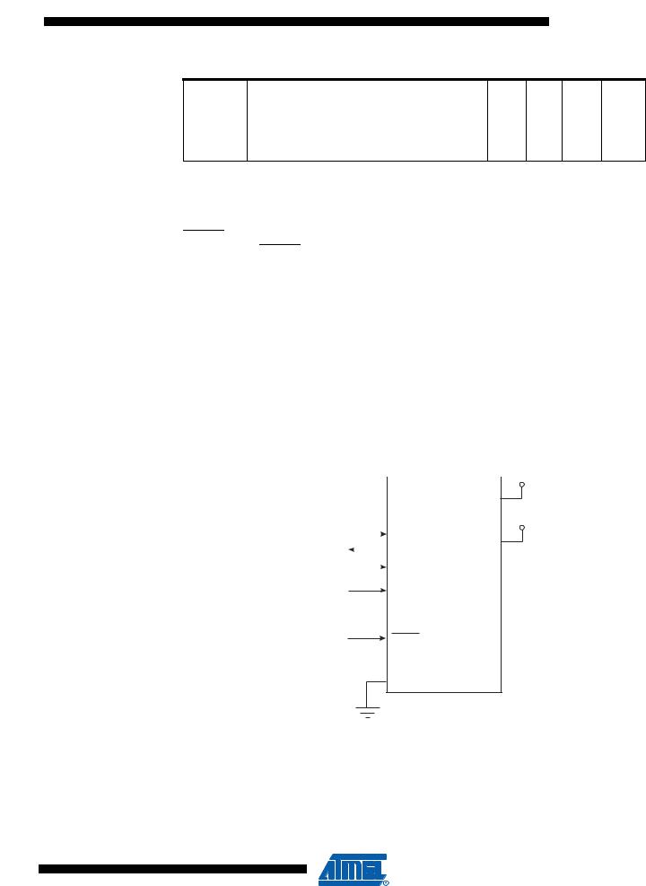
Figure 136. SPI Serial Programming and Verify(1)
|
|
|
|
|
|
|
|
|
+2.7 - 5.5V |
|
|
|
|
|
|
|
|
|
|
|
|
|
|
|
|
|
|
VCC |
|
|
|
|
|
|
|
|
|
|
+2.7 - 5.5V(2) |
MOSI |
|
|
|
PB5 |
|||||
|
|
||||||||
MISO |
|
|
|
AVCC |
|||||
|
|
|
PB6 |
||||||
|
|
|
|||||||
|
SCK |
|
|
|
PB7 |
||||
|
|
||||||||
|
|
|
|
|
|
|
|
XTAL1 |
|
|
|
|
|
|
|
|
|
||
RESET
GND
Notes: 1. If the device is clocked by the Internal Oscillator, it is no need to connect a clock source to the XTAL1 pin.
2. VCC -0.3V < AVCC < VCC +0.3V, however, AVCC should always be within 2.7 - 5.5V
When programming the EEPROM, an auto-erase cycle is built into the self-timed programming operation (in the serial mode ONLY) and there is no need to first execute the Chip Erase instruc-
273
2466P–AVR–08/07