

- •Features
- •Disclaimer
- •Overview
- •Block Diagram
- •Pin Descriptions
- •Port A (PA7..PA0)
- •Port B (PB7..PB0)
- •Port C (PC7..PC0)
- •Port D (PD7..PD0)
- •RESET
- •XTAL1
- •XTAL2
- •AVCC
- •AREF
- •Resources
- •Data Retention
- •AVR CPU Core
- •Introduction
- •Status Register
- •Stack Pointer
- •I/O Memory
- •Clock Systems and their Distribution
- •Clock Sources
- •Crystal Oscillator
- •External Clock
- •Idle Mode
- •Power-down Mode
- •Power-save Mode
- •Standby Mode
- •Analog Comparator
- •Brown-out Detector
- •Watchdog Timer
- •Port Pins
- •Resetting the AVR
- •Reset Sources
- •Power-on Reset
- •External Reset
- •Watchdog Reset
- •Watchdog Timer
- •Interrupts
- •I/O Ports
- •Introduction
- •Configuring the Pin
- •Reading the Pin Value
- •Unconnected pins
- •Alternate Port Functions
- •Register Description for I/O Ports
- •8-bit Timer/Counter0 with PWM
- •Overview
- •Registers
- •Definitions
- •Counter Unit
- •Normal Mode
- •Fast PWM Mode
- •8-bit Timer/Counter Register Description
- •Timer/Counter0 and Timer/Counter1 Prescalers
- •Internal Clock Source
- •Prescaler Reset
- •External Clock Source
- •16-bit Timer/Counter1
- •Overview
- •Registers
- •Definitions
- •Compatibility
- •Counter Unit
- •Input Capture Unit
- •Noise Canceler
- •Force Output Compare
- •Normal Mode
- •Fast PWM Mode
- •16-bit Timer/Counter Register Description
- •8-bit Timer/Counter2 with PWM and Asynchronous Operation
- •Overview
- •Registers
- •Definitions
- •Counter Unit
- •Normal Mode
- •Fast PWM Mode
- •8-bit Timer/Counter Register Description
- •Slave Mode
- •Master Mode
- •Data Modes
- •USART
- •Overview
- •Clock Generation
- •External Clock
- •Frame Formats
- •Parity Bit Calculation
- •Parity Generator
- •Receiver Error Flags
- •Parity Checker
- •Disabling the Receiver
- •Using MPCM
- •Write Access
- •Read Access
- •Features
- •TWI Terminology
- •Transferring Bits
- •Address Packet Format
- •Data Packet Format
- •Overview of the TWI Module
- •SCL and SDA Pins
- •Bus Interface Unit
- •Address Match Unit
- •Control Unit
- •Using the TWI
- •Master Receiver Mode
- •Slave Receiver Mode
- •Miscellaneous States
- •Analog Comparator Multiplexed Input
- •Analog to Digital Converter
- •Features
- •Operation
- •Changing Channel or Reference Selection
- •ADC Input Channels
- •Analog Input Circuitry
- •Features
- •Overview
- •TAP Controller
- •PRIVATE0; $8
- •PRIVATE1; $9
- •PRIVATE2; $A
- •PRIVATE3; $B
- •Bibliography
- •IEEE 1149.1 (JTAG) Boundary-scan
- •Features
- •System Overview
- •Data Registers
- •Bypass Register
- •Reset Register
- •EXTEST; $0
- •IDCODE; $1
- •AVR_RESET; $C
- •BYPASS; $F
- •Scanning the ADC
- •ATmega16 Boundary-scan Order
- •Features
- •Application Section
- •Read-While-Write and no Read- While-Write Flash Sections
- •Prevent Reading the RWW Section during Self-Programming
- •Simple Assembly Code Example for a Boot Loader
- •Fuse Bits
- •Latching of Fuses
- •Signature Bytes
- •Calibration Byte
- •Page Size
- •Signal Names
- •Chip Erase
- •Reading the Flash
- •Reading the EEPROM
- •Data Polling Flash
- •Data Polling EEPROM
- •AVR_RESET ($C)
- •PROG_ENABLE ($4)
- •Data Registers
- •Reset Register
- •Programming Enable Register
- •Programming Command Register
- •Virtual Flash Page Read Register
- •Performing Chip Erase
- •Reading the Flash
- •Reading the EEPROM
- •Electrical Characteristics
- •Absolute Maximum Ratings*
- •DC Characteristics
- •External Clock Drive Waveforms
- •External Clock Drive
- •Two-wire Serial Interface Characteristics
- •ADC Characteristics
- •Idle Supply Current
- •Pin Pullup
- •Pin Driver Strength
- •Register Summary
- •Instruction Set Summary
- •Ordering Information
- •Packaging Information
- •Errata
Two-wire Serial
Interface
Features
•Simple Yet Powerful and Flexible Communication Interface, Only Two Bus Lines Needed
•Both Master and Slave Operation Supported
•Device Can Operate as Transmitter or Receiver
•7-bit Address Space allows up to 128 Different Slave Addresses
•Multi-master Arbitration Support
•Up to 400 kHz Data Transfer Speed
•Slew-rate Limited Output Drivers
•Noise Suppression Circuitry Rejects Spikes on Bus Lines
•Fully Programmable Slave Address with General Call Support
•Address Recognition causes Wake-up when AVR is in Sleep Mode
Two-wire Serial
Interface Bus
Definition
The Two-wire Serial Interface (TWI) is ideally suited for typical microcontroller applications. The TWI protocol allows the systems designer to interconnect up to 128 different devices using only two bi-directional bus lines, one for clock (SCL) and one for data (SDA). The only external hardware needed to implement the bus is a single pull-up resistor for each of the TWI bus lines. All devices connected to the bus have individual addresses, and mechanisms for resolving bus contention are inherent in the TWI protocol.
Figure 76. TWI Bus Interconnection
VCC
Device 1 |
|
|
|
Device 3 |
|
|
|
|
|
|
|
Device 2 |
|
........ |
Device n |
|
R1 |
|
R2 |
||
|
|
|
|
|
|
|
|
|
|
|
|
|
|
|
|
|
|
|
|
|
|
SDA
SCL
TWI Terminology |
The following definitions are frequently encountered in this section. |
|
|
Table 72. TWI Terminology |
|
|
|
|
|
Term |
Description |
|
|
|
|
Master |
The device that initiates and terminates a transmission. The Master also |
|
|
generates the SCL clock. |
|
|
|
|
Slave |
The device addressed by a Master. |
|
|
|
|
Transmitter |
The device placing data on the bus. |
|
|
|
|
Receiver |
The device reading data from the bus. |
|
|
|
172 ATmega16(L)
2466P–AVR–08/07
 ATmega16(L)
Electrical |
As depicted in Figure 76, both bus lines are connected to the positive supply voltage through |
Interconnection |
pull-up resistors. The bus drivers of all TWI-compliant devices are open-drain or open-collector. |
|
This implements a wired-AND function which is essential to the operation of the interface. A low |
|
level on a TWI bus line is generated when one or more TWI devices output a zero. A high level |
|
is output when all TWI devices tri-state their outputs, allowing the pull-up resistors to pull the line |
|
high. Note that all AVR devices connected to the TWI bus must be powered in order to allow any |
|
bus operation. |
|
The number of devices that can be connected to the bus is only limited by the bus capacitance |
|
limit of 400 pF and the 7-bit Slave address space. A detailed specification of the electrical char- |
|
acteristics of the TWI is given in “Two-wire Serial Interface Characteristics” on page 294. Two |
|
different sets of specifications are presented there, one relevant for bus speeds below 100 kHz, |
|
and one valid for bus speeds up to 400 kHz. |
Data Transfer and
Frame Format
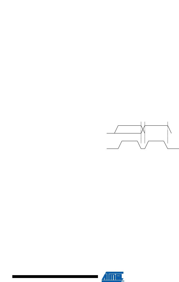
Transferring Bits |
Each data bit transferred on the TWI bus is accompanied by a pulse on the clock line. The level |
||
|
of the data line must be stable when the clock line is high. The only exception to this rule is for |
||
|
generating start and stop conditions. |
|
|
|
Figure 77. Data Validity |
|
|
|
SDA |
|
|
|
SCL |
|
|
|
|
|
|
|
Data Stable |
Data Stable |
|
|
Data Change |
||
START and STOP |
The Master initiates and terminates a data transmission. The transmission is initiated when the |
||
Conditions |
Master issues a START condition on the bus, and it is terminated when the Master issues a |
||
|
STOP condition. Between a START and a STOP condition, the bus is considered busy, and no |
||
|
other Master should try to seize control of the bus. A special case occurs when a new START |
||
|
condition is issued between a START and STOP condition. This is referred to as a REPEATED |
||
|
START condition, and is used when the Master wishes to initiate a new transfer without releas- |
||
ing control of the bus. After a REPEATED START, the bus is considered busy until the next STOP. This is identical to the START behavior, and therefore START is used to describe both START and REPEATED START for the remainder of this datasheet, unless otherwise noted. As depicted below, START and STOP conditions are signalled by changing the level of the SDA line when the SCL line is high.
173
2466P–AVR–08/07
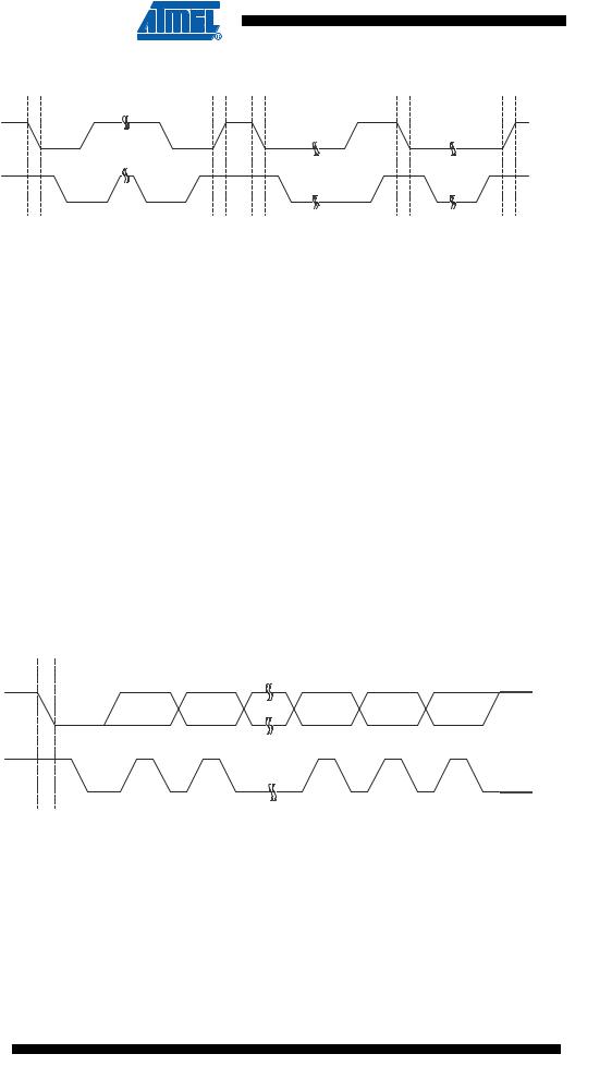
Figure 78. START, REPEATED START, and STOP Conditions
|
SDA |
|
|
|
|
SCL |
|
|
|
|
START |
STOP START |
REPEATED START |
STOP |
Address Packet |
All address packets transmitted on the TWI bus are nine bits long, consisting of seven address |
|||
Format |
bits, one READ/WRITE control bit and an acknowledge bit. If the READ/WRITE bit is set, a read |
|||
|
operation is to be performed, otherwise a write operation should be performed. When a Slave |
|||
|
recognizes that it is being addressed, it should acknowledge by pulling SDA low in the ninth SCL |
|||
|
(ACK) cycle. If the addressed Slave is busy, or for some other reason can not service the Mas- |
|||
|
ter’s request, the SDA line should be left high in the ACK clock cycle. The Master can then |
|||
|
transmit a STOP condition, or a REPEATED START condition to initiate a new transmission. An |
|||
address packet consisting of a Slave address and a READ or a WRITE bit is called SLA+R or SLA+W, respectively.
The MSB of the address byte is transmitted first. Slave addresses can freely be allocated by the designer, but the address 0000 000 is reserved for a general call.
When a general call is issued, all Slaves should respond by pulling the SDA line low in the ACK cycle. A general call is used when a Master wishes to transmit the same message to several Slaves in the system. When the general call address followed by a Write bit is transmitted on the bus, all Slaves set up to acknowledge the general call will pull the SDA line low in the ack cycle. The following data packets will then be received by all the Slaves that acknowledged the general call. Note that transmitting the general call address followed by a Read bit is meaningless, as this would cause contention if several Slaves started transmitting different data.
All addresses of the format 1111 xxx should be reserved for future purposes.
Figure 79. Address Packet Format
Addr MSB |
|
Addr LSB R/W |
ACK |
|
|
|
|
SDA
SCL
1 |
2 |
7 |
8 |
9 |
START
174 ATmega16(L)
2466P–AVR–08/07
 ATmega16(L)
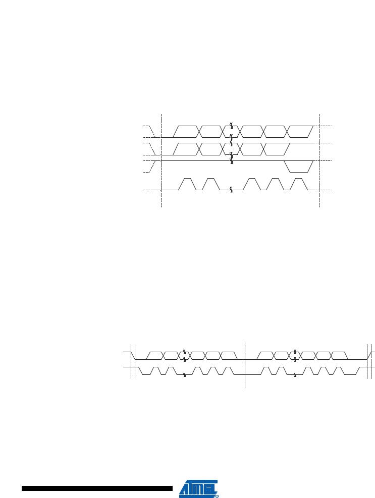
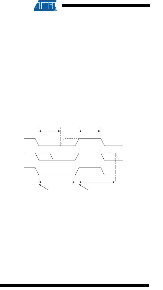
Data Packet Format All data packets transmitted on the TWI bus are nine bits long, consisting of one data byte and an acknowledge bit. During a data transfer, the Master generates the clock and the START and STOP conditions, while the receiver is responsible for acknowledging the reception. An Acknowledge (ACK) is signalled by the receiver pulling the SDA line low during the ninth SCL cycle. If the receiver leaves the SDA line high, a NACK is signalled. When the receiver has received the last byte, or for some reason cannot receive any more bytes, it should inform the transmitter by sending a NACK after the final byte. The MSB of the data byte is transmitted first.
Figure 80. Data Packet Format
Data MSB |
Data LSB ACK |
Aggregate
SDA
SDA from
Transmitter
SDA from receiverR
SCL from
Master
1 |
2 |
7 |
8 |
9 |
STOP, REPEATED |
|
|
|
|
|
|
SLA+R/W |
|
Data Byte |
|
|
START or Next |
|
|
|
|
|
Data Byte |
Combining Address A transmission basically consists of a START condition, a SLA+R/W, one or more data packets and Data Packets into and a STOP condition. An empty message, consisting of a START followed by a STOP condi- a Transmission tion, is illegal. Note that the wired-ANDing of the SCL line can be used to implement handshaking between the Master and the Slave. The Slave can extend the SCL low period by pulling the SCL line low. This is useful if the clock speed set up by the Master is too fast for the Slave, or the Slave needs extra time for processing between the data transmissions. The Slave extending the SCL low period will not affect the SCL high period, which is determined by the Master. As a consequence, the Slave can reduce the TWI data transfer speed by prolonging the
SCL duty cycle.
Figure 81 shows a typical data transmission. Note that several data bytes can be transmitted between the SLA+R/W and the STOP condition, depending on the software protocol implemented by the application software.
Figure 81. Typical Data Transmission
Addr MSB |
|
Addr LSB |
R/W |
ACK |
Data MSB |
|
|
Data LSB |
ACK |
SDA |
|
|
|
|
|
|
|
|
|
SCL |
|
|
|
|
|
|
|
|
|
1 |
2 |
7 |
8 |
9 |
1 |
2 |
7 |
8 |
9 |
START |
|
SLA+R/W |
|
|
|
Data Byte |
|
|
STOP |
175
2466P–AVR–08/07
Multi-master Bus
Systems,
Arbitration and
Synchronization
The TWI protocol allows bus systems with several Masters. Special concerns have been taken in order to ensure that transmissions will proceed as normal, even if two or more Masters initiate a transmission at the same time. Two problems arise in multi-master systems:
•An algorithm must be implemented allowing only one of the Masters to complete the transmission. All other Masters should cease transmission when they discover that they have lost the selection process. This selection process is called arbitration. When a contending Master discovers that it has lost the arbitration process, it should immediately switch to Slave mode to check whether it is being addressed by the winning Master. The fact that multiple Masters have started transmission at the same time should not be detectable to the Slaves, i.e., the data being transferred on the bus must not be corrupted.
•Different Masters may use different SCL frequencies. A scheme must be devised to synchronize the serial clocks from all Masters, in order to let the transmission proceed in a lockstep fashion. This will facilitate the arbitration process.
The wired-ANDing of the bus lines is used to solve both these problems. The serial clocks from all Masters will be wired-ANDed, yielding a combined clock with a high period equal to the one from the Master with the shortest high period. The low period of the combined clock is equal to the low period of the Master with the longest low period. Note that all Masters listen to the SCL line, effectively starting to count their SCL high and low time-out periods when the combined SCL line goes high or low, respectively.
Figure 82. SCL Synchronization between Multiple Masters
TA low |
TA high |
SCL from
Master A
SCL from
Master B
SCL bus
Line
TBlow |
|
|
TBhigh |
|
|||
|
|||
Masters Start |
Masters Start |
||
Counting Low Period |
Counting High Period |
||
Arbitration is carried out by all Masters continuously monitoring the SDA line after outputting data. If the value read from the SDA line does not match the value the Master had output, it has lost the arbitration. Note that a Master can only lose arbitration when it outputs a high SDA value while another Master outputs a low value. The losing Master should immediately go to Slave mode, checking if it is being addressed by the winning Master. The SDA line should be left high, but losing Masters are allowed to generate a clock signal until the end of the current data or address packet. Arbitration will continue until only one Master remains, and this may take many bits. If several Masters are trying to address the same Slave, arbitration will continue into the data packet.
176 ATmega16(L)
2466P–AVR–08/07
ATmega16(L)
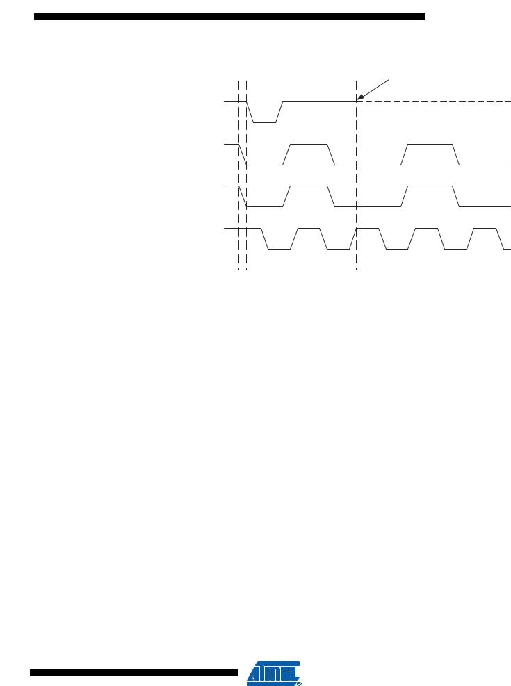
Figure 83. Arbitration between Two Masters
START
SDA from
Master A
SDA from
Master B
SDA Line
Synchronized
SCL Line
Note that arbitration is not allowed between:
Master A Loses
Arbitration, SDAA SDA
SDA
•A REPEATED START condition and a data bit
•A STOP condition and a data bit
•A REPEATED START and a STOP condition
It is the user software’s responsibility to ensure that these illegal arbitration conditions never occur. This implies that in multi-master systems, all data transfers must use the same composition of SLA+R/W and data packets. In other words: All transmissions must contain the same number of data packets, otherwise the result of the arbitration is undefined.
177
2466P–AVR–08/07