

 ATmega16(L)
8-bit Timer/Counter0 with PWM
Timer/Counter0 is a general purpose, single compare unit, 8-bit Timer/Counter module. The main features are:
•Single Compare Unit Counter
•Clear Timer on Compare Match (Auto Reload)
•Glitch-free, Phase Correct Pulse Width Modulator (PWM)
•Frequency Generator
•External Event Counter
•10-bit Clock Prescaler
•Overflow and Compare Match Interrupt Sources (TOV0 and OCF0)
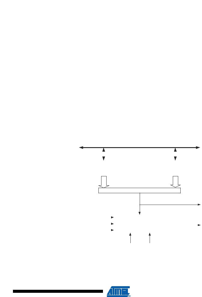
Overview |
A simplified block diagram of the 8-bit Timer/Counter is shown in Figure 27. For the actual place- |
|
ment of I/O pins, refer to “Pinout ATmega16” on page 2. CPU accessible I/O Registers, including |
|
I/O bits and I/O pins, are shown in bold. The device-specific I/O Register and bit locations are |
|
listed in the “8-bit Timer/Counter Register Description” on page 83. |
|
Figure 27. 8-bit Timer/Counter Block Diagram |
DATABUS

|
TCCRn |
|
|
count |
|
|
TOVn |
clear |
Control Logic |
|
(Int.Req.) |
direction |
Clock Select |
|
|
clkTn |
|
||
|
|
Edge |
Tn |
|
|
Detector |
|
|
|
|
|
BOTTOM |
TOP |
|
|
Timer/Counter |
|
( From Prescaler ) |
|
|
|
|
|
TCNTn |
= 0xFF |
|
|
= 0 |
|
OCn |
|
|
|
|
|
|
|
|
(Int.Req.) |
= |
|
Waveform |
OCn |
|
Generation |
||
|
|
|
OCRn
Registers |
The Timer/Counter (TCNT0) and Output Compare Register (OCR0) are 8-bit registers. Interrupt |
||||
|
request (abbreviated to Int.Req. in the figure) signals are all visible in the Timer Interrupt Flag |
||||
|
Register (TIFR). All interrupts are individually masked with the Timer Interrupt Mask Register |
||||
|
(TIMSK). TIFR and TIMSK are not shown in the figure since these registers are shared by other |
||||
|
timer units. |
||||
|
The Timer/Counter can be clocked internally, via the prescaler, or by an external clock source on |
||||
|
the T0 pin. The Clock Select logic block controls which clock source and edge the Timer/Counter |
||||
|
uses to increment (or decrement) its value. The Timer/Counter is inactive when no clock source |
||||
|
is selected. The output from the Clock Select logic is referred to as the timer clock (clkT0). |
||||
|
The double buffered Output Compare Register (OCR0) is compared with the Timer/Counter |
||||
|
value at all times. The result of the compare can be used by the waveform generator to generate |
||||
|
a PWM or variable frequency output on the Output Compare Pin (OC0). See “Output Compare |
||||
|
|
|
|
|
|
|
|
|
|
|
71 |
|
|
|
|
|
|
|
|
|
|
|
|
2466P–AVR–08/07
|
|
|
|
|
|
|
|
|
|
|
|
|
|
|
|
|
Unit” on page 73. for details. The compare match event will also set the Compare Flag (OCF0) |
||||||
|
which can be used to generate an output compare interrupt request. |
||||||
Definitions |
Many register and bit references in this document are written in general form. A lower case “n” |
||||||
|
replaces the Timer/Counter number, in this case 0. However, when using the register or bit |
||||||
|
defines in a program, the precise form must be used i.e., TCNT0 for accessing Timer/Counter0 |
||||||
|
counter value and so on. |
||||||
|
The definitions in Table 37 are also used extensively throughout the document. |
||||||
|
Table 37. Definitions |
||||||
|
|
|
|
|
|
|
|
|
BOTTOM |
The counter reaches the BOTTOM when it becomes 0x00. |
|
||||
|
MAX |
The counter reaches its MAXimum when it becomes 0xFF (decimal 255). |
|
||||
|
TOP |
The counter reaches the TOP when it becomes equal to the highest |
|
||||
|
|
value in the count sequence. The TOP value can be assigned to be the |
|
||||
|
|
fixed value 0xFF (MAX) or the value stored in the OCR0 Register. The |
|
||||
|
|
assignment is dependent on the mode of operation. |
|
||||
|
|
|
|
|
|
|
|
Timer/Counter
Clock Sources
Counter Unit
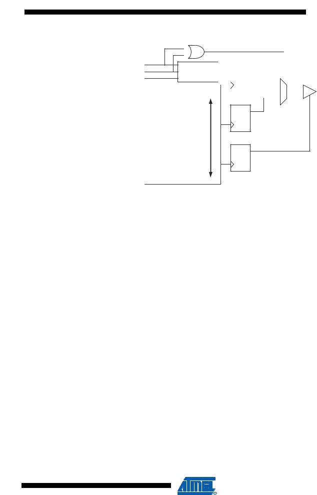
The Timer/Counter can be clocked by an internal or an external clock source. The clock source is selected by the clock select logic which is controlled by the clock select (CS02:0) bits located in the Timer/Counter Control Register (TCCR0). For details on clock sources and prescaler, see “Timer/Counter0 and Timer/Counter1 Prescalers” on page 87.
The main part of the 8-bit Timer/Counter is the programmable bi-directional counter unit. Figure 28 shows a block diagram of the counter and its surroundings.
Figure 28. Counter Unit Block Diagram
|
|
|
|
|
|
|
|
|
|
TOVn |
|
|
|||||||||
|
DATA BUS |
|
|
|
|
|
|
|
|
(Int. Req.) |
|
|
|||||||||
|
|
|
|
|
|
|
|
|
|
|
|
|
|
|
|
|
|
|
|
|
|
|
|
|
|
|
|
|
|
|
|
|
|
|
|
|
Clock Select |
|
|
||||
|
|
|
|
count |
|
|
|
|
|
|
|
|
|
|
|
|
|
|
|
|
|
|
|
|
|
|
|
|
|
|
|
|
|
|
|
Edge |
|
|
|
Tn |
|||
|
|
|
|
clear |
|
|
|
|
|
clkTn |
|
|
|
Detector |
|
|
|
|
|||
|
|
|
|
|
|
|
|
|
|
|
|
|
|
|
|
||||||
|
TCNTn |
|
|
Control Logic |
|
|
|
|
|
|
|
|
|
|
|||||||
|
|
|
direction |
|
|
|
|
|
|
|
|
|
|
|
|
||||||
|
|
|
|
|
|
|
|
|
|
|
|
|
|
|
|
|
|
|
|
|
|
|
|
|
|
|
|
|
|
|
|
|
|
|
|
|
|
|
|
|
|
|
|
|
|
|
|
|
|
|
|
|
|
|
|
|
|
|
( From Prescaler ) |
|
|
|
|||
|
|
|
|
|
|
|
|
|
|
|
|
||||||||||
|
|
|
|
|
|
|
|
|
|
|
|
|
|
|
|
|
|
|
|
||
|
|
|
|
|
|
|
|
|
|
|
|
|
|
|
|
|
|
|
|
|
|
|
|
|
|
BOTTOM |
|
TOP |
|
|
|||||||||||||
|
|
|
|
|
|
|
|
|
|
|
|
|
|
|
|
|
|
|
|
|
|
Signal description (internal signals):
count |
Increment or decrement TCNT0 by 1. |
direction |
Select between increment and decrement. |
clear |
Clear TCNT0 (set all bits to zero). |
clkTn |
Timer/Counter clock, referred to as clkT0 in the following. |
TOP |
Signalize that TCNT0 has reached maximum value. |
BOTTOM |
Signalize that TCNT0 has reached minimum value (zero). |
Depending of the mode of operation used, the counter is cleared, incremented, or decremented at each timer clock (clkT0). clkT0 can be generated from an external or internal clock source, selected by the Clock Select bits (CS02:0). When no clock source is selected (CS02:0 = 0) the timer is stopped. However, the TCNT0 value can be accessed by the CPU, regardless of
72 ATmega16(L) 
2466P–AVR–08/07
 ATmega16(L)
Output Compare
Unit
whether clkT0 is present or not. A CPU write overrides (has priority over) all counter clear or count operations.
The counting sequence is determined by the setting of the WGM01 and WGM00 bits located in the Timer/Counter Control Register (TCCR0). There are close connections between how the counter behaves (counts) and how waveforms are generated on the Output Compare output OC0. For more details about advanced counting sequences and waveform generation, see “Modes of Operation” on page 76.
The Timer/Counter Overflow (TOV0) Flag is set according to the mode of operation selected by the WGM01:0 bits. TOV0 can be used for generating a CPU interrupt.
The 8-bit comparator continuously compares TCNT0 with the Output Compare Register (OCR0). Whenever TCNT0 equals OCR0, the comparator signals a match. A match will set the Output Compare Flag (OCF0) at the next timer clock cycle. If enabled (OCIE0 = 1 and Global Interrupt Flag in SREG is set), the Output Compare Flag generates an output compare interrupt. The OCF0 Flag is automatically cleared when the interrupt is executed. Alternatively, the OCF0 Flag can be cleared by software by writing a logical one to its I/O bit location. The waveform generator uses the match signal to generate an output according to operating mode set by the WGM01:0 bits and Compare Output mode (COM01:0) bits. The max and bottom signals are used by the waveform generator for handling the special cases of the extreme values in some modes of operation (See “Modes of Operation” on page 76.).
Figure 29 shows a block diagram of the output compare unit.
Figure 29. Output Compare Unit, Block Diagram
DATA BUS
|
|
|
|
|
|
|
|
|
|
OCRn |
|
TCNTn |
||
|
|
|
|
|
= (8-bit Comparator )
OCFn (Int.Req.)
top |
|
|
|
|
|
|
|
bottom |
|
|
Waveform Generator |
|
|
|
|
|
|
|
|
OCn |
|||
FOCn |
|
|
|
|
|||
|
|
|
|
|
|||
|
|
|
|
|
|
||
|
|
|
|
|
|
|
|
WGMn1:0 COMn1:0
The OCR0 Register is double buffered when using any of the Pulse Width Modulation (PWM) modes. For the normal and Clear Timer on Compare (CTC) modes of operation, the double buffering is disabled. The double buffering synchronizes the update of the OCR0 Compare Register to either top or bottom of the counting sequence. The synchronization prevents the occurrence of odd-length, non-symmetrical PWM pulses, thereby making the output glitch-free.
73
2466P–AVR–08/07

|
|
|
|
|
|
|
|
|
|
|
|
|
The OCR0 Register access may seem complex, but this is not case. When the double buffering |
||||
|
is enabled, the CPU has access to the OCR0 Buffer Register, and if double buffering is disabled |
||||
|
the CPU will access the OCR0 directly. |
||||
Force Output |
In non-PWM waveform generation modes, the match output of the comparator can be forced by |
||||
Compare |
writing a one to the Force Output Compare (FOC0) bit. Forcing compare match will not set the |
||||
|
OCF0 Flag or reload/clear the timer, but the OC0 pin will be updated as if a real compare match |
||||
|
had occurred (the COM01:0 bits settings define whether the OC0 pin is set, cleared or toggled). |
||||
Compare Match |
All CPU write operations to the TCNT0 Register will block any compare match that occur in the |
||||
Blocking by TCNT0 |
next timer clock cycle, even when the timer is stopped. This feature allows OCR0 to be initialized |
||||
Write |
to the same value as TCNT0 without triggering an interrupt when the Timer/Counter clock is |
||||
|
enabled. |
||||
Using the Output |
Since writing TCNT0 in any mode of operation will block all compare matches for one timer clock |
||||
Compare Unit |
cycle, there are risks involved when changing TCNT0 when using the output compare unit, inde- |
||||
|
pendently of whether the Timer/Counter is running or not. If the value written to TCNT0 equals |
||||
|
the OCR0 value, the compare match will be missed, resulting in incorrect waveform generation. |
||||
|
Similarly, do not write the TCNT0 value equal to BOTTOM when the counter is downcounting. |
||||
|
The setup of the OC0 should be performed before setting the Data Direction Register for the port |
||||
|
pin to output. The easiest way of setting the OC0 value is to use the Force Output Compare |
||||
|
(FOC0) strobe bits in Normal mode. The OC0 Register keeps its value even when changing |
||||
|
between waveform generation modes. |
||||
|
Be aware that the COM01:0 bits are not double buffered together with the compare value. |
||||
|
Changing the COM01:0 bits will take effect immediately. |
||||
Compare Match |
The Compare Output mode (COM01:0) bits have two functions. The Waveform Generator uses |
||||
Output Unit |
the COM01:0 bits for defining the Output Compare (OC0) state at the next compare match. Also, |
||||
|
the COM01:0 bits control the OC0 pin output source. Figure 30 shows a simplified schematic of |
||||
|
the logic affected by the COM01:0 bit setting. The I/O Registers, I/O bits, and I/O pins in the fig- |
||||
|
ure are shown in bold. Only the parts of the general I/O port Control Registers (DDR and PORT) |
||||
|
that are affected by the COM01:0 bits are shown. When referring to the OC0 state, the reference |
||||
|
is for the internal OC0 Register, not the OC0 pin. If a System Reset occur, the OC0 Register is |
||||
|
reset to “0”. |
||||
74 ATmega16(L) 
2466P–AVR–08/07
ATmega16(L)
Figure 30. Compare Match Output Unit, Schematic
COMn1
COMn0 Waveform
FOCn Generator
DATA BUS
clkI/O
|
|
|
|
|
|
|
|
|
|
|
|
|
|
|
|
|
|
|
|
|
|
|
|
D Q |
|
|
|
|
|
|
|
|
|
|
|
|
|
|
|
|
|
|
|
|
|
|
|
|
|
|
|
|
|
|
|
|
|
|
|
1 |
|
|
|
|
|
|
|
|
|
|
|
|
|
|
|
OCn |
|
|
OCn |
|
|
0 |
|
|
|
Pin |
|
|
|
|
|
|
|
|
|
|
||
 D Q
D Q
PORT
 D Q
D Q
DDR
The general I/O port function is overridden by the Output Compare (OC0) from the Waveform Generator if either of the COM01:0 bits are set. However, the OC0 pin direction (input or output) is still controlled by the Data Direction Register (DDR) for the port pin. The Data Direction Register bit for the OC0 pin (DDR_OC0) must be set as output before the OC0 value is visible on the pin. The port override function is independent of the Waveform Generation mode.
The design of the output compare pin logic allows initialization of the OC0 state before the output is enabled. Note that some COM01:0 bit settings are reserved for certain modes of operation. See “8-bit Timer/Counter Register Description” on page 83.
Compare Output Mode The Waveform Generator uses the COM01:0 bits differently in normal, CTC, and PWM modes.
and Waveform |
For all modes, setting the COM01:0 = 0 tells the waveform generator that no action on the OC0 |
Generation |
Register is to be performed on the next compare match. For compare output actions in the non- |
|
PWM modes refer to Table 39 on page 84. For fast PWM mode, refer to Table 40 on page 84, |
|
and for phase correct PWM refer to Table 41 on page 84. |
|
A change of the COM01:0 bits state will have effect at the first compare match after the bits are |
|
written. For non-PWM modes, the action can be forced to have immediate effect by using the |
|
FOC0 strobe bits. |
75
2466P–AVR–08/07