

Розрахункова СЗіВІ / Розрахункова робота / Стабілізатори напруги / LDO National Semiconductor / LP2966
.pdfMarch 2005
LP2966
Dual 150mA Ultra Low-Dropout Regulator
General Description
The LP2966 dual ultra low-dropout (LDO) regulator operates from a +2.70V to +7.0V input supply. Each output delivers 150mA over full temperature range. The IC operates with extremely low drop-out voltage and quiescent current, which makes it very suitable for battery powered and portable applications. Each LDO in the LP2966 has independent shutdown capability. The LP2966 provides low noise performance with low ground pin current in an extremely small MSOP-8 package (refer to package dimensions and connection diagram for more information on MSOP-8 package). A wide range of preset voltage options are available for each output. In addition to the voltage combinations listed in the ordering information table, many more are available upon request with minimum orders. In all, 256 voltage combinations are possible.
Features
n Ultra low drop-out voltage n Low ground pin current
n <1µA quiescent current in shutdown mode
n Independent shutdown of each LDO regulator n Output voltage accuracy ±1%
n Guaranteed 150mA output current at each output n Low output noise
n Error Flags indicate status of each output
n Available in MSOP-8 surface mount packages n Low output capacitor requirements (1µF)
nOperates with Low ESR ceramic capacitors in most applications
n Over temperature/over current protection
n -40ûC to +125ûC junction temperature range
Key Specifications
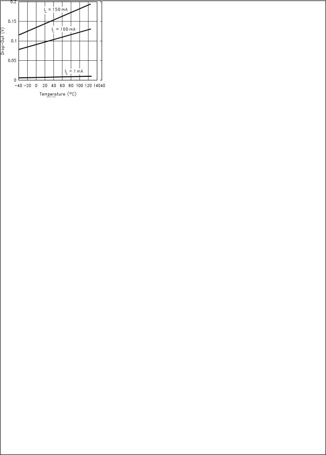
Dropout Voltage: Varies linearly with load current. Typically 0.9 mV at 1mA load current and 135mV at 150mA load current.
Ground Pin Current: Typically 300µA at 1mA load current and 340µA at 100mA load current (with one shutdown pin pulled low).
Shutdown Mode: Less than 1µA quiescent current when both shutdown pins are pulled low.
Error Flag: Open drain output, goes low when the corresponding output drops 10% below nominal.
Precision Output Voltage: Multiple output voltage options available ranging from 1.8V to 5.0V with a guaranteed accuracy of ±1% at room temperature.
Applications
n Cellular and Wireless Applications n Palmtop/Laptop Computer
n GPS systems
n Flat panel displays n Post regulators
n USB applications
n Hand held equipment and multimeters n Wireless data terminals
n Other battery powered applications
Typical Application Circuit
10085030
*SD1 and SD2 must be actively terminated through a pull up resistor. Tie to VIN if not used.
**ERROR1 and ERROR2 are open drain outputs. These pins must be connected to ground if not used.
# Minimum output capacitance is 1µF to insure stability over full load current range. More capacitance improves superior dynamic performance and provides additional stability margin.
Regulator Dropout-Low Ultra 150mA Dual LP2966
© 2005 National Semiconductor Corporation |
DS100850 |
www.national.com |
LP2966
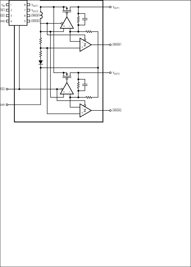
Block Diagram
10085031
Connection Diagram
10085032
Top View
Mini SO-8 Package
8-Lead Small Outline Integrated Circuit (SOIC)
Package Code: MSOP-8
www.national.com |
2 |

Pin Description
Pin |
|
|
Name |
Function |
|
|
|
|
|
|
|
1 |
VIN |
Input Supply pin |
|||
|
|
|
|
|
|
2 |
|
|
Active low shutdown pin for output 1 |
||
|
SD1 |
|
|
||
|
|
|
|
|
|
3 |
|
|
Active low shutdown pin for output 2 |
||
|
SD2 |
|
|
||
4 |
GND |
Ground |
|||
|
|
|
|
|
|
5 |
|
Error flag for output 2 - Normally high impedance, should be connected to ground if not |
|||
|
ERROR2 |
|
|||
|
|
|
|
|
used. |
|
|
|
|
|
|
6 |
|
Error flag for output 1 - Normally high impedance, should be connected to ground if not |
|||
|
ERROR1 |
|
|||
|
|
|
|
|
used. |
|
|
|
|
|
|
7 |
VOUT2 |
Output 2 |
|||
|
|
|
|
|
|
8 |
VOUT1 |
Output 1 |
|||
|
|
|
|
|
|
TABLE 1. Ordering Information
The following voltage options and their combinations are possible. 5.0V, 4.0V, 3.8V, 3.6V, 3.3V, 3.2V, 3.1V, 3.0V, 2.9V, 2.8V, 2.7V, 2.6V, 2.5V, 2.4V, 2.0V and 1.8V
Output |
Output Voltage |
Order Number |
Package Marking |
Supplied As: |
Voltage 1 |
2 |
|
|
|
|
|
|
|
|
5.0 |
5.0 |
LP2966IMM-5050 |
LAFB |
1000 units on tape and reel |
|
|
|
|
|
5.0 |
5.0 |
LP2966IMMX-5050 |
LAFB |
3500 units on tape and reel |
|
|
|
|
|
3.6 |
3.6 |
LP2966IMM-3636 |
LAEB |
1000 units on tape and reel |
|
|
|
|
|
3.6 |
3.6 |
LP2966IMMX-3636 |
LAEB |
3500 units on tape and reel |
|
|
|
|
|
3.3 |
3.6 |
LP2966IMM-3336 |
LAHB |
1000 units on tape and reel |
|
|
|
|
|
3.3 |
3.6 |
LP2966IMMX-3336 |
LAHB |
3500 units on tape and reel |
|
|
|
|
|
3.3 |
3.3 |
LP2966IMM-3333 |
LADB |
1000 units on tape and reel |
|
|
|
|
|
3.3 |
3.3 |
LP2966IMMX-3333 |
LADB |
3500 units on tape and reel |
|
|
|
|
|
3.3 |
2.5 |
LP2966IMM-3325 |
LARB |
1000 units on tape and reel |
|
|
|
|
|
3.3 |
2.5 |
LP2966IMMX-3325 |
LARB |
3500 units on tape and reel |
|
|
|
|
|
3.0 |
3.0 |
LP2966IMM-3030 |
LACB |
1000 units on tape and reel |
|
|
|
|
|
3.0 |
3.0 |
LP2966IMMX-3030 |
LACB |
3500 units on tape and reel |
|
|
|
|
|
2.8 |
3.0 |
LP2966IMM-2830 |
LASB |
1000 units on tape and reel |
|
|
|
|
|
2.8 |
3.0 |
LP2966IMMX-2830 |
LASB |
3500 units on tape and reel |
|
|
|
|
|
2.8 |
2.8 |
LP2966IMM-2828 |
LABB |
1000 units on tape and reel |
|
|
|
|
|
2.8 |
2.8 |
LP2966IMMX-2828 |
LABB |
3500 units on tape and reel |
|
|
|
|
|
2.5 |
2.5 |
LP2966IMM-2525 |
LAAB |
1000 units on tape and reel |
|
|
|
|
|
2.5 |
2.5 |
LP2966IMMX-2525 |
LAAB |
3500 units on tape and reel |
|
|
|
|
|
2.5 |
1.8 |
LP2966IMM-2518 |
LJKB |
1000 units on tape and reel |
|
|
|
|
|
2.5 |
1.8 |
LP2966IMMX-2518 |
LJKB |
3500 units on tape and reel |
|
|
|
|
|
1.8 |
3.3 |
LP2966IMM-1833 |
LCFB |
1000 units on tape and reel |
|
|
|
|
|
1.8 |
3.3 |
LP2966IMMX-1833 |
LCFB |
3500 units on Tape and reel |
|
|
|
|
|
1.8 |
3.0 |
LP2966IMM-1830 |
LEYB |
1000 units on tape and reel |
|
|
|
|
|
1.8 |
3.0 |
LP2966IMMX-1830 |
LEYB |
3500 units on Tape and reel |
|
|
|
|
|
1.8 |
2.8 |
LP2966IMM-1828 |
LAVB |
1000 units on tape and reel |
|
|
|
|
|
1.8 |
2.8 |
LP2966IMMX-1828 |
LAVB |
3500 units on tape and reel |
|
|
|
|
|
1.8 |
1.8 |
LP2966IMM-1818 |
LA9B |
1000 units on tape and reel |
|
|
|
|
|
1.8 |
1.8 |
LP2966IMMX-1818 |
LA9B |
3500 units on tape and reel |
|
|
|
|
|
The voltage options and combinations shown in Table 1 are available. For other custom voltage options or combinations of voltage options, please contact your nearest National Semiconductor Sales Office.
LP2966
3 |
www.national.com |

LP2966
Absolute Maximum Ratings (Note 1)
If Military/Aerospace specified devices are required, please contact the National Semiconductor Sales Office/ Distributors for availability and specifications.
Storage Temperature Range |
−65 to +150ûC |
||
Lead Temp. (Soldering, 5 sec.) |
260ûC |
||
Power Dissipation (Note 2) |
Internally Limited |
||
ESD Rating (Note 3) |
2kV |
||
Input Supply Voltage (Survival) |
−0.3V to 7.5V |
||
Shutdown Input Voltage (Survival) |
−0.3V to (Vin + 0.3V) |
||
|
|
||
Maximum Voltage for |
ERROR |
Pins |
10V |
IOUT (Survival) |
Short Circuit Protected |
||
Output Voltage (Survival)(Note 6), |
−0.3V to (Vin + 0.3V) |
(Note 7) |
|
Operating Ratings (Note 1)
Input Supply Voltage |
2.7V to 7.0V |
||
Shutdown Input Voltage |
−0.3V to (Vin + 0.3V) |
||
Operating Junction |
−40ûC to +125ûC |
||
Temperature Range |
|
||
|
|
||
Maximum Voltage for |
ERROR |
|
10V |
pins |
|
||
Electrical Characteristics
Limits in standard typeface are for Tj = 25ûC, and limits in boldface type apply over the full operating junction temperature range. Unless otherwise specified, VIN = VO(NOM) + 1V, (Note 16), COUT = 1µF, IOUT = 1mA, CIN = 1µF, VSD1 = VSD2 = VIN.
Symbol |
Parameter |
Conditions |
Typ (Note |
LP2966IMM (Note 5) |
Unit |
||
4) |
|
|
|||||
Min |
Max |
||||||
|
|
|
|
||||
|
|
|
|
|
|
|
|
Vo |
Output Voltage |
VOUT + 1V < VIN < 7.0V |
0.0 |
−1 |
1 |
%VNOM |
|
(Note 13) |
Tolerance |
|
|
-3 |
3 |
||
|
|
|
|||||
|
|
|
|
|
|
|
|
|
|
1mA < IL < 100mA |
0.0 |
−1.5 |
1.5 |
%VNOM |
|
|
|
|
|
-3.5 |
3.5 |
||
|
|
|
|
|
|||
|
|
|
|
|
|
|
|
∆VO/∆VIN |
Output Voltage Line |
|
|
|
|
|
|
(Note 8) |
|
0.1 |
|
|
mV/V |
||
Regulation |
|
|
|
||||
(Note 13) |
|
|
|
|
|
||
|
|
|
|
|
|
||
|
|
|
|
|
|
|
|
∆VO/∆IOUT |
Output Voltage Load |
1mA < IL< 100mA |
0.1 |
|
|
mV/mA |
|
|
Regulation (Note 9) |
(Note 9) |
|
|
|||
|
|
|
|
|
|||
|
|
|
|
|
|
|
|
∆VO2/∆IOUT1 |
Output Voltage Cross |
1mA < IL1< 100mA |
0.0004 |
|
|
mV/mA |
|
|
Regulation (Note 10) |
(Note 10) |
|
|
|
||
|
|
|
|
|
|||
|
|
|
|
|
|
|
|
VIN -VOUT |
Dropout Voltage |
IL = 1mA |
0.9 |
|
2.0 |
|
|
|
(Note 12) |
|
|
|
3.0 |
|
|
|
|
|
|
|
|
|
|
|
|
IL = 100mA |
90 |
|
130 |
mV |
|
|
|
|
|
|
180 |
||
|
|
|
|
|
|
||
|
|
|
|
|
|
|
|
|
|
IL = 150mA |
135 |
|
195 |
|
|
|
|
|
|
|
270 |
|
|
|
|
|
|
|
|
|
|
IGND(1,0)(Note 18) |
Ground Pin Current |
IL = 1mA |
300 |
|
|
|
|
|
(One LDO On) |
VSD2 ≤ 0.1V, VSD1= VIN |
|
|
|
µA |
|
|
|
IL = 100mA |
340 |
|
|
||
|
|
|
|
|
|||
|
|
VSD2 ≤ 0.1V, VSD1= VIN |
|
|
|
|
|
IGND(1,1) |
Ground Pin Current |
IL = 1mA |
340 |
|
450 |
|
|
|
(Both LDOs On) |
|
|
|
500 |
µA |
|
|
|
|
|
|
|
||
|
|
IL = 100mA |
420 |
|
540 |
||
|
|
|
|
||||
|
|
|
|
|
600 |
|
|
|
|
|
|
|
|
|
|
IGND(0,0) |
Ground Pin Current |
VSD1= VSD2 ≤ 0.1V |
0.006 |
|
0.3 |
µA |
|
|
in Shutdown Mode |
|
|
|
10 |
||
|
|
|
|
|
|||
|
|
|
|
|
|
|
|
IO(PK) |
Peak Output Current |
(Note 2) |
500 |
350 |
|
mA |
|
|
|
VOUT≥ VOUT(NOM)- 5% |
|
150 |
|
||
|
|
|
|
|
|||
Short Circuit Foldback Protection |
|
|
|
|
|
||
|
|
|
|
|
|
|
|
IFB |
Short Circuit |
(Note 2), (Note 14) |
600 |
|
|
mA |
|
|
Foldback Knee |
|
|
|
|
|
|
|
|
|
|
|
|
|
|
Over Temperature Protection |
|
|
|
|
|
||
|
|
|
|
|
|
|
|
Tsh(t) |
Shutdown Threshold |
|
165 |
|
|
ûC |
|
|
|
|
|
|
|
|
|
www.national.com |
4 |

Electrical Characteristics (Continued)
Limits in standard typeface are for Tj = 25ûC, and limits in boldface type apply over the full operating junction temperature range. Unless otherwise specified, VIN = VO(NOM) + 1V, (Note 16), COUT = 1µF, IOUT = 1mA, CIN = 1µF, VSD1 = VSD2 = VIN.
Symbol |
Parameter |
Conditions |
Typ (Note |
LP2966IMM (Note 5) |
Unit |
||
4) |
|
|
|||||
Min |
Max |
||||||
|
|
|
|
||||
|
|
|
|
|
|
|
|
Tsh(h) |
Thermal Shutdown |
|
25 |
|
|
ûC |
|
|
Hysteresis |
|
|
|
|
||
|
|
|
|
|
|
||
|
|
|
|
|
|
|
|
Shutdown Input |
|
|
|
|
|
|
|
|
|
|
|
|
|
|
|
VSDT |
Shutdown Threshold |
Output = Low |
0 |
|
0.1 |
V |
|
|
(Note 15) |
Output = High |
VIN |
VIN - 0.1 |
|
||
|
|
|
|||||
TdOFF |
Turn-off Delay (Note |
IL = 100 mA |
20 |
|
|
µsec |
|
|
17) |
|
|
|
|
|
|
|
|
|
|
|
|
|
|
TdON |
Turn-on Delay (Note |
IL = 100 mA |
25 |
|
|
µsec |
|
|
17) |
|
|
|
|
|
|
|
|
|
|
|
|
|
|
ISD |
SD Input Current |
VSD = VIN |
1 |
|
|
nA |
|
|
|
VSD = 0 V |
1 |
|
|
||
|
|
|
|
|
|||
Error Flag Comparators |
|
|
|
|
|
||
|
|
|
|
|
|
|
|
VT |
Threshold (output |
|
10 |
5 |
16 |
% |
|
|
goes high to low) |
(Note 11) |
|
|
|
|
|
|
|
|
|
|
|
|
|
VTH |
Threshold Hysteresis |
|
5 |
2 |
8 |
% |
|
|
|
(Note 11) |
|
|
|
|
|
|
|
|
|
|
|
|
|
VERR(Sat) |
Error Flag Saturation |
IFsink = 100µA |
0.015 |
|
0.1 |
V |
|
IEF(leak) |
Error Flag Pin |
|
1 |
|
|
nA |
|
|
Leakage Current |
|
|
|
|
|
|
|
|
|
|
|
|
|
|
I(EFsink) |
Error Flag Pin Sink |
|
1 |
|
|
mA |
|
|
Current |
|
|
|
|
|
|
|
|
|
|
|
|
|
|
AC Parameters |
|
|
|
|
|
|
|
|
|
|
|
|
|
|
|
PSRR |
Ripple Rejection |
VIN = VOUT + 1V, f = |
60 |
|
|
|
|
|
|
120Hz, VOUT = 3.3V |
|
|
|
dB |
|
|
|
VIN = VOUT + 0.3V, f = |
40 |
|
|
||
|
|
|
|
|
|||
|
|
120Hz, VOUT = 3.3V |
|
|
|
|
|
ρn(1/f) |
Output Noise Density |
f =120Hz |
1 |
|
|
µV/√Hz |
|
en |
Output Noise Voltage |
BW = 10Hz − 100kHz, |
150 |
|
|
|
|
|
(rms) |
COUT = 10µF |
|
|
|
µV(rms) |
|
|
|
BW = 300Hz − 300kHz, |
100 |
|
|
||
|
|
|
|
|
|||
|
|
COUT = 10µF |
|
|
|
|
|
Note 1: Absolute maximum ratings indicate limits beyond which damage to the device may occur. Operating ratings indicate conditions for which the device is intended to be functional, but do not guarantee specific performance limits. For guaranteed specifications and test conditions, see Electrical characteristics. The guaranteed specifications apply only for the test conditions listed. Some performance characteristics may degrade when the device is not operated under the listed test conditions.
Note 2: At elevated temperatures, devices must be derated based on package thermal resistance. The device in the surface-mount package must be derated at θjA = 235ûC/W, junction-to-ambient. Please refer to the applications section on maximum current capability for further information. The device has internal thermal protection.
Note 3: The human body model is a 100pF capacitor discharged through a 1.5kΩ resistor into each pin.
Note 4: : Typical numbers are at 25ûC and represent the most likely parametric norm.
Note 5: : Limits are 100% production tested at 25ûC. Limits over the operating temperature range are guaranteed through correlation using Statistical Quality Control (SQC) methods. The limits are used to calculate NationalÕs Averaging Outgoing Quality Level (AOQL).
Note 6: If used in a dual-supply system where the regulator load is returned to a negative supply, the LP2966 output must be diode-clamped to ground.
Note 7: The output PMOS structure contains a diode between the VIN and VOUT terminals that is normally reverse-biased. Reversing the polarity from VIN and VOUT will turn on this diode.
Note 8: Output voltage line regulation is defined as the change in output voltage from the nominal value due to change in input line voltage.
Note 9: Output voltage load regulation is defined as the change in output voltage from the nominal value when the load current changes from 1mA to 100mA.
Note 10: Output voltage cross regulation is defined as the percentage change in the output voltage from the nominal value at one output when the load current
changes from 1mA to full load in the other output. This is an important parameter in multiple output regulators. The specification for ∆VO1/∆IOUT2 is equal to the specification for ∆VO2/∆IOUT1.
Note 11: Error Flag threshold and hysteresis are specified as the percentage below the regulated output voltage.
Note 12: Dropout voltage is defined as the input to output differential at which the output voltage drops 100mV below the nominal value. Drop-out voltage specification applies only to output voltages greater than 2.7V. For output voltages below 2.7V, the drop-out voltage is nothing but the input to output differential, since the minimum input voltage is 2.7V.
LP2966
5 |
www.national.com |

LP2966
Electrical Characteristics (Continued)
Note 13: Output voltage tolerance specification also includes the line regulation and load regulation.
Note 14: LP2966 has fold back current limited short circuit protection. The knee is the current at which the output voltage drops 10% below the nominal value.
Note 15: VSDT is the shutdown pin voltage threshold below which the output is disabled.
Note 16: The condition VIN = VO(NOM) + 1V applies when Vout1 = Vout2. If Vout1 ≠ Vout2, then this condition would apply to the output which is greater in value. As an example, if Vout1 = 3.3V and Vout2 = 5V, then the condition VIN = VO(NOM)+ 1V would apply to Vout2 only.
Note 17: Turn-on delay is the time interval between the low to high transition on the shutdown pin to the output voltage settling to within 5% of the nominal value. Turn-off delay is the time interval between the high to low transition on the shutdown pin to the output voltage dropping below 50% of the nominal value. The external load impedance influences the output voltage decay in shutdown mode.
Note 18: The limits for the ground pin current specification, IGND(0,1) will be same as the limits for the specification, IGND(1,0).
www.national.com |
6 |
Typical Performance Characteristics Unless otherwise specified, VIN =VO(NOM) + 1V, VOUT= 3.3V, COUT =1µF, IOUT = 1mA, CIN =1µF, VSD1 = VSD2 = VIN, and TA = 25ûC.
Ground Pin Current vs Supply Voltage (one LDO on) |
Ground Pin Current vs Supply Voltage (both LDOs on) |
10085001 |
10085002 |
Ground Pin Current vs Load Current over temperature |
Ground Pin Current vs Load Current over temperature |
(one LDO on) |
(both LDOs on) |
10085003 |
10085004 |
Output Voltage vs Temperature |
Drop-out Voltage vs Temperature |
10085005 |
10085006 |
LP2966
7 |
www.national.com |

LP2966
Typical Performance Characteristics Unless otherwise specified, VIN =VO(NOM) + 1V, VOUT= 3.3V, COUT =1µF, IOUT = 1mA, CIN =1µF, VSD1 = VSD2 = VIN, and TA = 25ûC. (Continued)
Input Voltage vs Output Voltage |
Ground Pin Current vs Shutdown Pin Voltage |
10085007 |
10085008 |
Ground Pin Current vs Input Voltage (Both LDOs off) |
Short-Circuit Foldback Protection |
10085009 |
10085010 |
Line Transient Response |
Line Transient Response |
(COUT = 2.2µF, IOUT = 1mA) |
(COUT = 2.2µF, IOUT = 1mA) |
10085018 |
10085019 |
www.national.com |
8 |

Typical Performance Characteristics Unless otherwise specified, VIN =VO(NOM) + 1V, VOUT= 3.3V, COUT =1µF, IOUT = 1mA, CIN =1µF, VSD1 = VSD2 = VIN, and TA = 25ûC. (Continued)
Line Transient Response |
Line Transient Response |
(COUT = 2.2µF, IOUT = 100mA) |
(COUT = 2.2µF, IOUT = 100mA) |
10085020 |
10085021 |
Line Transient Response |
Line Transient Response |
(COUT = 10µF, IOUT = 1mA) |
(COUT = 10µF, IOUT = 1mA) |
10085022 |
10085023 |
Line Transient Response |
Line Transient Response |
(COUT = 10µF, IOUT = 100mA) |
(COUT = 10µF, IOUT = 100mA) |
10085025 |
10085024 |
LP2966
9 |
www.national.com |

LP2966
Typical Performance Characteristics Unless otherwise specified, VIN =VO(NOM) + 1V, VOUT= 3.3V, COUT =1µF, IOUT = 1mA, CIN =1µF, VSD1 = VSD2 = VIN, and TA = 25ûC. (Continued)
Load Transient Response (COUT = 2.2µF) |
Load Transient Response (COUT = 10µF) |
10085026 |
10085027 |
Load Transient Response (COUT = 10µF) |
Load Transient Response (COUT = 2.2µF) |
10085028 |
10085029 |
Cross-Channel Isolation vs Frequency |
Cross-Channel Isolation vs Frequency |
(IOUT1 =1mA, IOUT2 = 1mA) |
(IOUT1 = IOUT2 = 100mA) |
10085015 |
10085016 |
www.national.com |
10 |