

Розрахункова СЗіВІ / Розрахункова робота / Стабілізатори напруги / LDO National Semiconductor / LP3879
.pdfJune 2006
LP3879
Micropower 800mA Low Noise "Ceramic Stable" Voltage Regulator for Low Voltage Applications
General Description
The LP3879 is a 800 mA fixed-output voltage regulator designed to provide high performance and low noise in applications requiring output voltages between 1.0V and 1.2V.
Using an optimized VIP™ (Vertically Integrated PNP) process, the LP3879 delivers superior performance:
Ground Pin Current: Typically 5.5 mA @ 800 mA load, and 200 µA @ 100 µA load.
Low Power Shutdown: The LP3879 draws less than 10 µA quiescent current when shutdown pin is pulled low.
Precision Output: Guaranteed output voltage accuracy is 1% at room temperature.
Low Noise: Broadband output noise is only 18 µV (typical) with 10 nF bypass capacitor.
Features
n Standard output voltage: 1.00V, 1.20V
nCustom voltages available from 1.0V to 1.2V (50 mV increments)
n Input voltage: 2.5 to 6V n 1% initial output accuracy
n Designed for use with low ESR ceramic capacitors n Very low output noise
n Sense option improves load regulation
n 8 Lead PSOP and LLP surface mount packages n <10 µA quiescent current in shutdown
n Low ground pin current at all loads n High peak current capability
n Over-temperature/over-current protection
n -40˚C to +125˚C junction temperature range
Applications
n ASIC Power Supplies In:
- Desktops, Notebooks and Graphic Cards
- Set Top Boxes, Printers and Copiers
n DSP and FPGA Power Supplies
n SMPS Post-Regulator
n Medical Instrumentation
Basic Application Circuit
20161303
*Capacitance values shown are minimum required to assure stability. Larger output capacitor provides improved dynamic response. Output capacitor must meet ESR requirements (see Application Information).
**The Shutdown pin must be actively terminated (see Application Information). Tie to INPUT (Pin 4) if not used.
VIP™ is a trademark of National Semiconductor Corporation.
Voltage Low for Regulator Voltage Stable" "Ceramic Noise Low 800mA Micropower LP3879
Applications
© 2006 National Semiconductor Corporation |
DS201613 |
www.national.com |

LP3879
Connection Diagrams
8 Lead PSOP Package (MRA) |
8 Lead LLP Surface Mount Package (SD) |
20161330
Top View
See NS Package Number MRA08A
20161350
Top View
See NS Package Number SDC08A
Ordering Information
TABLE 1. Package Marking and Ordering Information
Output Voltage |
Grade |
Order Information |
Supplied as: |
|
|
|
|
1.00 |
STD |
LP3879MR-1.0 |
95 Units per Rail |
|
|
|
|
1.00 |
STD |
LP3879MRX-1.0 |
2500 Units on Tape and Reel |
|
|
|
|
1.00 |
STD |
LP3879SD-1.0 |
1000 Units on Tape and Reel |
|
|
|
|
1.00 |
STD |
LP3879SDX-1.0 |
4500 Units on Tape and Reel |
|
|
|
|
1.20 |
STD |
LP3879MR-1.2 |
95 Units per Rail |
|
|
|
|
1.20 |
STD |
LP3879MRX-1.2 |
2500 Units on Tape and Reel |
|
|
|
|
1.20 |
STD |
LP3879SD-1.2 |
1000 Units on Tape and Reel |
|
|
|
|
1.20 |
STD |
LP3879SDX-1.2 |
4500 Units on Tape and Reel |
|
|
|
|
Pin Descriptions
Pin |
Name |
Function |
|
|
|
1 |
BYPASS |
The capacitor connected between BYPASS and GROUND lowers |
|
|
output noise voltage level and is required for loop stability. |
|
|
|
2 |
N/C |
DO NOT CONNECT. This pin is used for post package test and must |
|
|
be left floating. |
|
|
|
3 |
GROUND |
Device ground. |
|
|
|
4 |
INPUT |
Input source voltage. |
|
|
|
5 |
OUTPUT |
Regulated output voltage. |
|
|
|
6 |
SENSE |
Remote Sense. Tie directly to output or remotely at point of load for |
|
|
best regulation. |
|
|
|
7 |
N/C |
No internal connection. |
|
|
|
8 |
SHUTDOWN |
Output is enabled above turn-on threshold voltage. Pull down to turn off |
|
|
regulator output. |
|
|
|
PSOP, LLP |
SUBSTRATE |
The exposed die attach pad should be connected to a thermal pad at |
DAP |
GROUND |
ground potential. For additional information on using National |
|
|
Semiconductor’s Non Pull Back LLP package, please refer to LLP |
|
|
application note AN-1187 |
|
|
|
www.national.com |
2 |

Absolute Maximum Ratings (Note 1)
If Military/Aerospace specified devices are required, please contact the National Semiconductor Sales Office/ Distributors for availability and specifications.
Storage Temperature Range |
−65˚C to +150˚C |
|
Operating Junction |
Temperature |
|
Range |
|
-40˚C to +125˚C |
Lead Temperature |
(Soldering, 5 |
|
seconds) |
|
260˚C |
ESD Rating (Note 2) |
|
2 kV |
Shutdown Pin |
|
1kV |
Power Dissipation (Note 3) |
Internally Limited |
Input Supply Voltage (Survival) |
−0.3V to +16V |
Input Supply Voltage (Typical |
|
Operating) |
2.5V to +6V |
SENSE Pin |
−0.3V to +6V |
Output Voltage (Survival) (Note 4) |
−0.3V to +6V |
IOUT (Survival) |
Short Circuit |
|
Protected |
Input-Output Voltage (Survival) |
|
(Note 5) |
−0.3V to +16V |
Electrical Characteristics
Limits in standard typeface are for TJ = 25˚C, and limits in boldface type apply over the temperature range of -40˚C to 125˚C. Limits are guaranteed through design, testing, or correlation. The limits are used to calculate National’s Average Outgoing
Quality Level (AOQL). Unless otherwise specified: VIN = 3.0V, VOUT = 1V, IL = 1 mA, COUT = 10 µF, CIN = 4.7 µF, VS/D = 2V, CBYPASS = 10 nF.
Symbol |
Parameter |
Conditions |
Min |
Typical |
Max |
Units |
|
(Note 6) |
(Note 7) |
(Note 6) |
|||||
|
|
|
|
||||
|
|
|
|
|
|
|
|
VO |
Output Voltage |
|
-1.0 |
1.00 |
1.0 |
|
|
|
Tolerance |
1 mA ≤ IL ≤ 800 mA |
-2.0 |
1.00 |
2.0 |
%Vnom |
|
|
|
3.0V ≤ VIN ≤ 6V |
-3.0 |
3.0 |
|
||
|
|
|
|
||||
|
Output Voltage Line |
3.0V ≤ VIN ≤ 6V |
|
0.007 |
0.014 |
%/V |
|
|
Regulation |
|
|
0.032 |
|||
|
|
|
|
|
|
||
|
|
|
|
|
|
|
|
|
|
IL = 800 mA |
|
2.5 |
3.1 |
|
|
|
|
VOUT ≥ VOUT(NOM) - 1% |
|
|
|||
|
Minimum Input |
|
|
|
|
||
|
IL = 800 mA |
|
|
|
|
||
|
Voltage Required |
|
|
|
|
||
VIN (min) |
VOUT ≥ VOUT(NOM) - 1% |
|
2.5 |
2.8 |
V |
||
To Maintain Output |
|
||||||
|
0 ≤ TJ ≤ 125˚C |
|
|
|
|
||
|
Regulation |
|
|
|
|
||
|
IL = 750 mA |
|
2.5 |
3.0 |
|
||
|
|
|
|
||||
|
|
VOUT ≥ VOUT(NOM) - 1% |
|
|
|||
|
|
|
|
|
|
||
IGND |
Ground Pin Current |
IL = 100 µA |
|
200 |
250 |
µA |
|
|
|
|
|
275 |
|||
|
|
|
|
|
|
||
|
|
|
|
|
|
|
|
|
|
IL = 200 mA |
|
1.5 |
2 |
|
|
|
|
|
|
3.3 |
|
||
|
|
|
|
|
mA |
||
|
|
|
|
|
|
||
|
|
IL = 800 mA |
|
5.5 |
8.5 |
||
|
|
|
|
||||
|
|
|
|
15 |
|
||
|
|
|
|
|
|
||
|
|
|
|
|
|
|
|
IO(PK) |
Peak Output |
VOUT ≥ VOUT(NOM) − 5% |
|
1200 |
|
|
|
|
Current |
|
|
|
|
||
|
|
|
|
|
mA |
||
|
|
|
|
|
|
||
IO(MAX) |
Short Circuit |
RL = 0 (Steady State) |
|
1400 |
|
||
|
|
|
|||||
|
Current |
|
|
|
|
||
|
|
|
|
|
|
||
|
|
|
|
|
|
|
|
en |
Output Noise |
BW = 100 Hz to 100 kHz |
|
18 |
|
µV(RMS) |
|
|
Voltage (RMS) |
CBYPASS = 10 nF |
|
|
|||
|
|
|
|
|
|||
|
Ripple Rejection |
f = 1 kHz |
|
|
|
|
|
|
|
|
|
60 |
|
dB |
|
|
|
|
|
|
|
|
LP3879
3 |
www.national.com |
LP3879
Electrical Characteristics (Continued)
Limits in standard typeface are for TJ = 25˚C, and limits in boldface type apply over the temperature range of -40˚C to 125˚C. Limits are guaranteed through design, testing, or correlation. The limits are used to calculate National’s Average Outgoing
Quality Level (AOQL). Unless otherwise specified: VIN = 3.0V, VOUT = 1V, IL = 1 mA, COUT = 10 µF, CIN = 4.7 µF, VS/D = 2V, CBYPASS = 10 nF.
Symbol |
Parameter |
Conditions |
Min |
Typical |
Max |
Units |
|
(Note 6) |
(Note 7) |
(Note 6) |
|||||
|
|
|
|
||||
|
|
|
|
|
|
|
|
SHUTDOWN INPUT |
|
|
|
|
|
||
|
|
|
|
|
|
|
|
VS/D |
S/D Input Voltage |
VH = Output ON |
|
1.4 |
1.6 |
|
|
|
|
VL = Output OFF |
0.1 |
0.50 |
|
|
|
|
|
IIN ≤ 10 µA |
|
V |
|||
|
|
|
|
|
|||
|
|
VOUT ≤ 10 mV |
|
0.6 |
|
|
|
|
|
IIN ≤ 50 µA |
|
|
|
||
|
|
|
|
|
|
||
IS/D |
S/D Input Current |
VS/D = 0 |
|
0.02 |
−1 |
µA |
|
|
|
VS/D = 5V |
|
5 |
15 |
||
|
|
|
|
||||
Note 1: Absolute Maximum Ratings indicate limits beyond which damage to the component may occur. Electrical specifications do not apply when operating the device outside of its rated operating conditions.
Note 2: ESD testing was performed using Human Body Model, a 100 pF capacitor discharged through a 1.5 kΩ resistor.
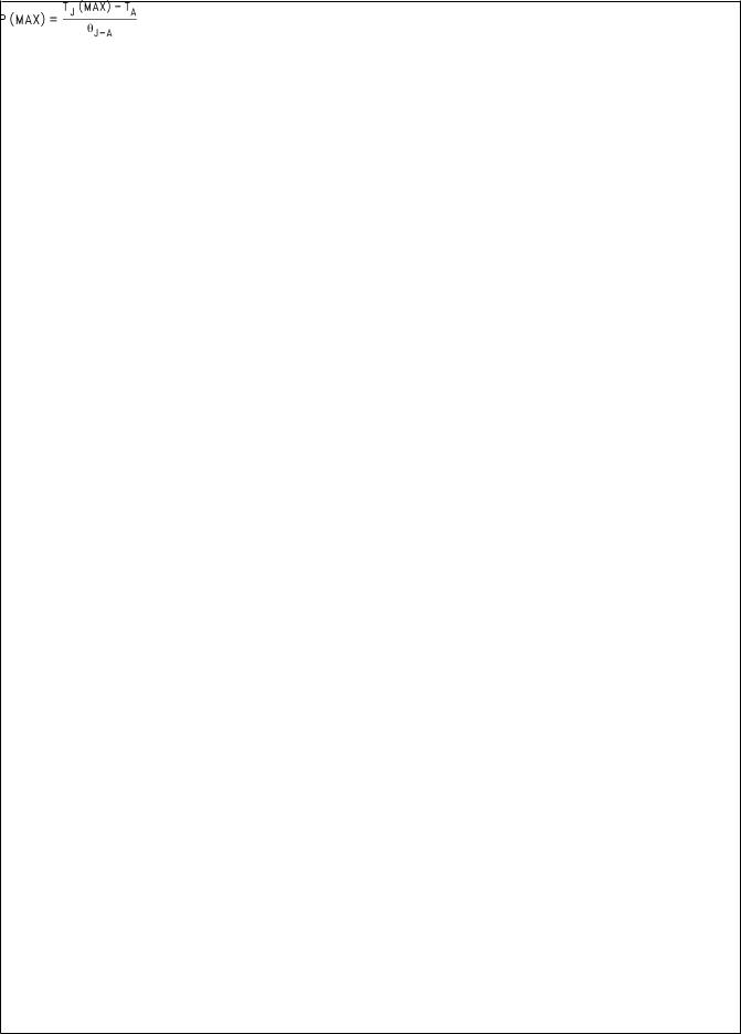
Note 3: The maximum allowable power dissipation is a function of the maximum junction temperature, TJ(MAX), the junction-to-ambient thermal resistance, θJ−A, and the ambient temperature, TA. The maximum allowable power dissipation at any ambient temperature is calculated using:
The value of θJ−A for the LLP (SD) and PSOP (MRA) packages are specifically dependent on PCB trace area, trace material, and the number of layers and thermal vias. If a four layer board is used with maximum vias from the IC center to the heat dissipating copper layers, values of θJ−A which can be obtained are approximately 60˚C/W for the PSOP-8 and 40˚C/W for the LLP-8 package. Exceeding the maximum allowable power dissipation will cause excessive die temperature, and the regulator will go into thermal shutdown.
Note 4: If used in a dual-supply system where the regulator load is returned to a negative supply, the LP3879 output must be diode-clamped to ground.
Note 5: The output PNP structure contains a diode between the VIN and VOUT terminals that is normally reverse-biased. Forcing the output above the input will turn on this diode and may induce a latch-up mode which can damage the part (see Application Hints).
Note 6: Limits are guaranteed through testing, statistical correlation, or design.
Note 7: Typical numbers reperesent the most likely norm for 25˚C operation.
www.national.com |
4 |

Typical Performance Characteristics Unless otherwise specified: VIN = 3.3V, VOUT = 1V, IL = 1 mA, CIN = 4.7 µF, COUT = 10 µF, VS/D = 2V, CBYP = 10 nF, TJ = 25˚C.
IGND vs Temperature |
Minimum VIN Over Temperature |
20161321
|
20161320 |
IGND vs ILoad |
VOUT vs Temperature |
|
20161322 |
20161359 |
|
|
|
VOUT vs Temperature |
|
Ripple Rejection |
20161328
20161354
LP3879
5 |
www.national.com |
LP3879
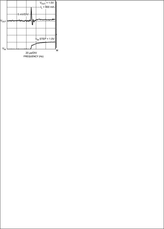
Typical Performance Characteristics Unless otherwise specified: VIN = 3.3V, VOUT = 1V, IL = 1 mA, CIN = 4.7 µF, COUT = 10 µF, VS/D = 2V, CBYP = 10 nF, TJ = 25˚C. (Continued)
Ripple Rejection |
Line Transient Response |
20161331
|
20161358 |
Line Transient Response |
Line Transient Response |
20161333 |
20161332 |
Line Transient Response |
Line Transient Response |
20161335 |
20161336 |
www.national.com |
6 |
Typical Performance Characteristics Unless otherwise specified: VIN = 3.3V, VOUT = 1V, IL = 1 mA, CIN = 4.7 µF, COUT = 10 µF, VS/D = 2V, CBYP = 10 nF, TJ = 25˚C. (Continued)
Line Transient Response |
Load Transient Response |
20161334 |
20161345 |
Load Transient Response |
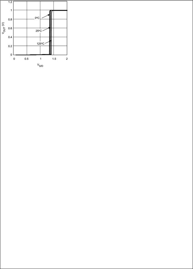
Turn-On Characteristics |
20161343
20161355
LP3879
7 |
www.national.com |
LP3879
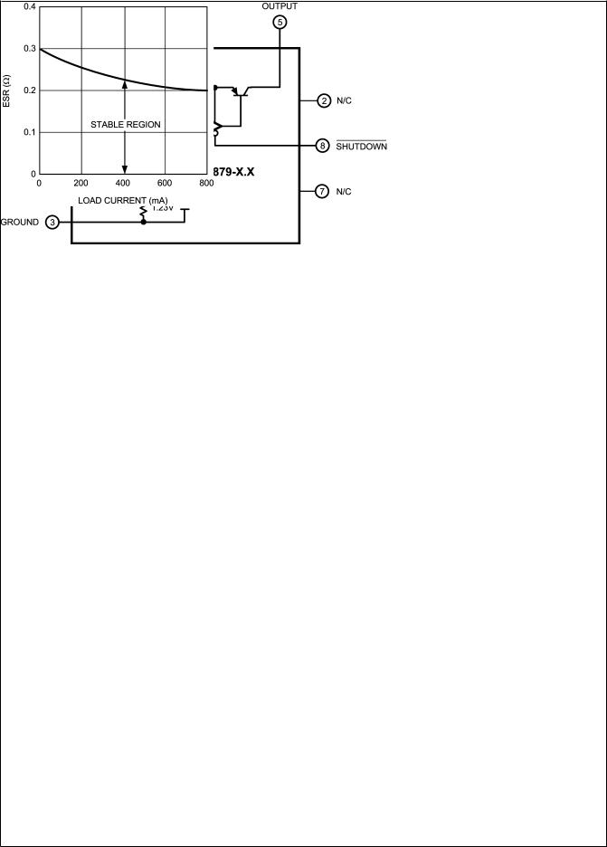
Block Diagram
Application Information
PACKAGE INFORMATION
The LP3879 is offered in the 8 lead PSOP or LLP surface mount packages to allow for increased power dissipation compared to the SO-8 and Mini SO-8.
EXTERNAL CAPACITORS
Like any low-dropout regulator, the LP3879 requires external capacitors for regulator stability. These capacitors must be correctly selected for good performance.
INPUT CAPACITOR: A capacitor whose value is at least 4.7 µF (±20%) is required between the LP3879 input and ground. A good quality X5R / X7R ceramic capacitor should be used.
Capacitor tolerance and temperature variation must be considered when selecting a capacitor (see Capacitor Characteristics section) to assure the minimum requirement of input capacitance is met over all operating conditions.
The input capacitor must be located not more than 0.5" from the input pin and returned to a clean analog ground. Any good quality ceramic or tantalum capacitor may be used, assuming the minimum input capacitance requirement is met.
OUTPUT CAPACITOR: The LP3879 requires a ceramic output capacitor whose size is at least 10 µF (±20%). A good quality X5R / X7R ceramic capacitor should be used. Capacitance tolerance and temperature characteristics must be considered when selecting an output capacitor.
The LP3879 is designed specifically to work with ceramic output capacitors, utilizing circuitry which allows the regulator to be stable across the entire range of output current with an ultra low ESR output capacitor.
The output capacitor selected must meet the requirement for minimum amount of capacitance and also have an ESR (equivalent series resistance) value which is within the stable range. A curve is provided which shows the stable ESR range as a function of load current (see Figure 1).
20161301
20161338
FIGURE 1. Stable Region For Output Capacitor ESR
Important: The output capacitor must maintain its ESR within the stable region over the full operating temperature range of the application to assure stability.
The output capacitor ESR forms a zero which is required to add phase lead near the loop gain crossover frequency, typically in the range of 50kHz to 200 kHz. The ESR at lower frequencies is of no importance. Some capacitor manufacturers list ESR at low frequencies only, and some give a formula for Dissipation Factor which can be used to calculate a value for a term referred to as ESR. However, since the DF formula is usually at a much lower frequency than the range listed above, it will give an unrealistically high value. If good quality X5R or X7R ceramic capacitors are used, the actual ESR in the 50 kHz to 200 kHz range will not exceed 25 milli Ohms. If these are used as output capacitors for the LP3879, the regulator stability requirements are satisfied.
It is important to remember that capacitor tolerance and variation with temperature must be taken into consideration
www.national.com |
8 |

Application Information (Continued)
when selecting an output capacitor so that the minimum required amount of output capacitance is provided over the full operating temperature range. (See Capacitor Characteristics section).
The output capacitor must be located not more than 0.5" from the output pin and returned to a clean analog ground.
NOISE BYPASS CAPACITOR: The 10 nF capacitor on the Bypass pin significantly reduces noise on the regulator output and is required for loop stability. However, the capacitor is connected directly to a high-impedance circuit in the bandgap reference.
Because this circuit has only a few microamperes flowing in it, any significant loading on this node will cause a change in the regulated output voltage. For this reason, DC leakage current through the noise bypass capacitor must never exceed 100 nA, and should be kept as low as possible for best output voltage accuracy.
The types of capacitors best suited for the noise bypass capacitor are ceramic and film. High-quality ceramic capacitors with either NPO or COG dielectric typically have very low leakage. 10 nF polypropolene and polycarbonate film capacitors are available in small surface-mount packages and typically have extremely low leakage current.
CAPACITOR CHARACTERISTICS
CERAMIC: The LP3879 was designed to work with ceramic capacitors on the output to take advantage of the benefits they offer: for capacitance values in the 10 µF range, ceramics are the least expensive and also have the lowest ESR values (which makes them best for eliminating highfrequency noise). The ESR of a typical 10 µF ceramic capacitor is in the range of 5 mΩ to 10 mΩ, which meets the ESR limits required for stability by the LP3879.
One disadvantage of ceramic capacitors is that their capacitance can vary with temperature. Many large value ceramic capacitors (≥ 2.2 µF) are manufactured with the Z5U or Y5V
temperature characteristic, which results in the capacitance dropping by more than 50% as the temperature goes from 25˚C to 85˚C.
Another significant problem with Z5U and Y5V dielectric devices is that the capacitance drops severely with applied voltage. A typical Z5U or Y5V capacitor can lose 60% of its rated capacitance with half of the rated voltage applied to it.
For these reasons, X7R and X5R type ceramic capacitors must be used on the input and output of the LP3879.
SHUTDOWN INPUT OPERATION
The LP3879 is shut off by pulling the Shutdown input low, and turned on by pulling it high. If this feature is not to be used, the Shutdown input should be tied to VIN to keep the regulator output on at all times.
To assure proper operation, the signal source used to drive the Shutdown input must be able to swing above and below the specified turn-on/turn-off voltage thresholds listed in the Electrical Characteristics section under VON/OFF.
REVERSE INPUT-OUTPUT VOLTAGE
The PNP power transistor used as the pass element in the LP3879 has an inherent diode connected between the regulator output and input.
During normal operation (where the input voltage is higher than the output) this diode is reverse-biased.
However, if the output is pulled above the input, this diode will turn ON and current will flow into the regulator output.
In such cases, a parasitic SCR can latch which will allow a high current to flow into VIN (and out the ground pin), which can damage the part.
In any application where the output may be pulled above the input, an external Schottky diode must be connected from
VIN to VOUT (cathode on VIN, anode on VOUT), to limit the reverse voltage across the LP3879 to 0.3V (see Absolute
Maximum Ratings).
LP3879
9 |
www.national.com |
LP3879
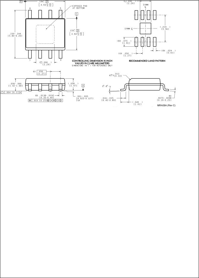
Physical Dimensions inches (millimeters) unless otherwise noted
8 Lead LLP Surface Mount PackagePackage
NS Package Number SDC08A
8-Lead PSOP Package (PSOP-8)
NS Package Number MRA08A
www.national.com |
10 |