

Розрахункова СЗіВІ / Розрахункова робота / Стабілізатори напруги / LDO National Semiconductor / LP3999
.pdfJuly 2006
LP3999
Low Noise 150mA Voltage Regulator for RF/Analog
Applications
General Description
The LP3999 regulator is designed to meet the requirements of portable wireless battery-powered applications and will provide an accurate output voltage with low noise and low quiescent current. Ideally suited for powering RF/Analog devices this device will also be used to meet more general circuit requirements.
For battery powered applications the low dropout and low ground current provided by the device allows the lifetime of the battery to be maximized.The inclusion of an Enable(disable) control can be used by the system to further extend the battery lifetime by reducing the power consumption to virtually zero. Should the application require a device with an active disable function please refer to device LP3995.
The LP3999 also features internal protection against shortcircuit currents and over-temperature conditions.
The LP3999 is designed to be stable with small 1.0 µF ceramic capacitors. The small outline of the LP3999 micro SMD package with the required ceramic capacitors can realize a system application within minimal board area.
Performance is specified for a −40˚C to +125˚C temperature range.
The device is available in micro SMD package. For other package options contact your local NSC sales office.
The device is available in fixed output voltages in the ranges of 1.5V to 3.3V. For availability, please contact your local NSC sales office.
Key Specifications
n 2.5V to 6.0V Input Range
n Accurate Output Voltage; ±75mV / 2%
n 60 mV Typical Dropout with 150 mA Load. Vout > 2.5V n Virtually Zero Quiescent Current when Disabled
n 10 µVrms output noise over 10Hz to 100kHz n Stable with a 1 µF Output Capacitor
n Guaranteed 150 mA Output Current n Fast Turn-on Time; 140 µs (Typ.)
Features
n 5 pin micro SMD Package
n Stable with Ceramic Capacitor n Logic Controlled Enable
n Fast Turn-on
n Thermal-overload and short-circuit protection
n −40 to +125˚C junction temperature range for operation
Applications
n GSM Portable Phones
n CDMA Cellular Handsets
n Wideband CDMA Cellular Handsets
n Bluetooth Devices
n Portable Information Appliances
n Handheld MP3 Devices
Typical Application Circuit
20052001
Applications RF/Analog for Regulator Voltage 150mA Noise Low LP3999
© 2006 National Semiconductor Corporation |
DS200520 |
www.national.com |
LP3999
Block Diagram
20052002
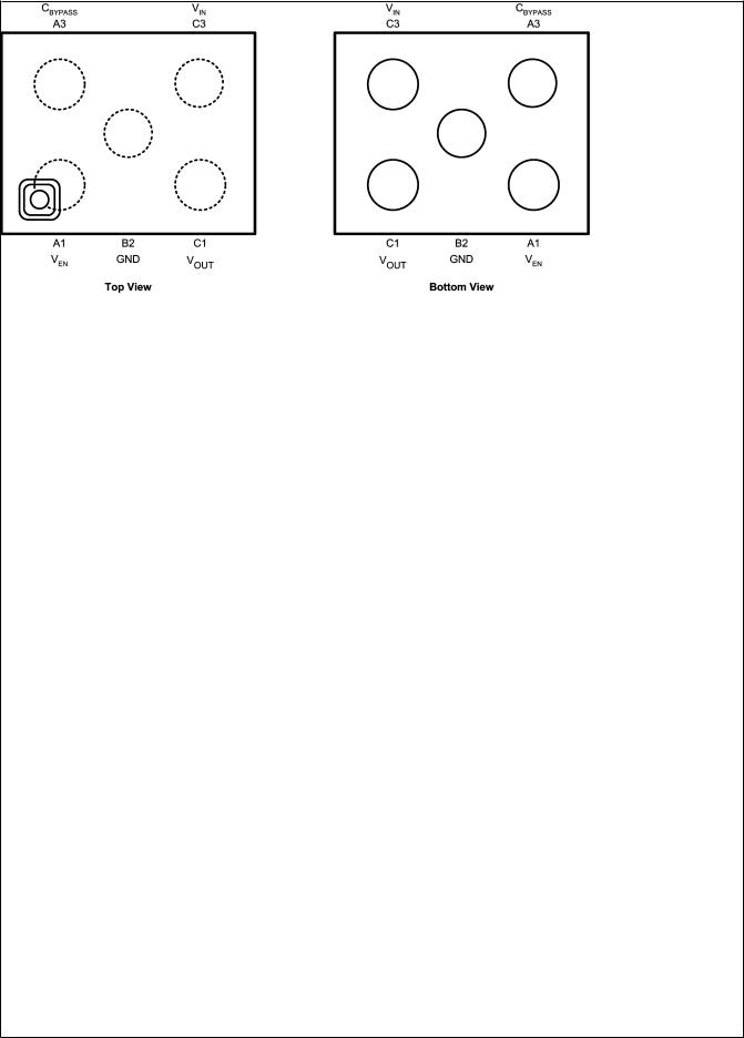
Pin Descriptions
Package 5–pin microSMD
Pin No. |
Symbol |
Name and Function |
|
|
|
A1 |
VEN |
Enable Input; Disables the Regulator when ≤ 0.4V. |
|
|
Enables the regulator when ≥ 0.9V |
|
|
|
B2 |
GND |
Common Ground |
|
|
|
C1 |
VOUT |
Voltage output. Connect this output to the load circuit. |
C3 |
VIN |
Voltage Supply Input |
A3 |
CBYPASS |
Bypass Capacitor connection. |
|
|
Connect a 0.01 µF capacitor for noise reduction. |
|
|
|
Connection Diagram
micro SMD, 5 Bump Package
20052003
See NS Package Number TLA05
www.national.com |
2 |

Ordering Information
For micro SMD Package
Output Voltage |
Grade |
LP3999 Supplied as 250 |
LP3999 Supplied as |
Package |
(V) |
|
Units, Tape and Reel |
3000 Units, Tape and |
Marking |
|
|
|
Reel |
|
|
|
|
|
|
1.5 |
STD |
LP3999ITL-1.5 |
LP3999ITLX-1.5 |
|
|
|
|
|
|
1.8 |
STD |
LP3999ITL-1.8 |
LP3999ITLX-1.8 |
|
|
|
|
|
|
1.875 |
STD |
LP3999ITL-1.875 |
LP3999ITLX-1.875 |
|
|
|
|
|
|
2.4 |
STD |
LP3999ITL-2.4 |
LP3999ITLX-2.4 |
|
|
|
|
|
|
2.5 |
STD |
LP3999ITL-2.5 |
LP3999ITLX-2.5 |
|
|
|
|
|
|
2.8 |
STD |
LP3999ITL-2.8 |
LP3999ITLX-2.8 |
|
|
|
|
|
|
3.3 |
STD |
LP3999ITL-3.3 |
LP3999ITLX-3.3 |
|
|
|
|
|
|
|
|
For micro SMD Package UNLEADED |
|
|
|
|
|
|
|
Output Voltage |
Grade |
LP3999 Supplied as 250 |
LP3999 Supplied as |
Package |
(V) |
|
Units, Tape and Reel |
3000 Units, Tape and |
Marking |
|
|
|
Reel |
|
|
|
|
|
|
1.5 |
STD |
LP3999ITL-1.5 NOPB |
LP3999ITLX-1.5 NOPB |
|
|
|
|
|
|
1.8 |
STD |
LP3999ITL-1.8 NOPB |
LP3999ITLX-1.8 NOPB |
|
|
|
|
|
|
1.875 |
STD |
LP3999ITL-1.875 NOPB |
LP3999ITLX-1.875 NOPB |
|
|
|
|
|
|
2.4 |
STD |
LP3999ITL-2.4 NOPB |
LP3999ITLX-2.4 NOPB |
|
|
|
|
|
|
2.5 |
STD |
LP3999ITL-2.5 NOPB |
LP3999ITLX-2.5 NOPB |
|
|
|
|
|
|
2.8 |
STD |
LP3999ITL-2.8 NOPB |
LP3999ITLX-2.8 NOPB |
|
|
|
|
|
|
3.3 |
STD |
LP3999ITL-3.3 NOPB |
LP3999ITLX-3.3 NOPB |
|
|
|
|
|
|
LP3999
3 |
www.national.com |

LP3999
Absolute Maximum Ratings
(Notes 1, 2)
If Military/Aerospace specified devices are required, please contact the National Semiconductor Sales Office/ Distributors for availability and specifications.
Input Voltage (VIN) |
−0.3 to 6.5V |
Output Voltage |
−0.3 to (VIN + 0.3V) |
|
to 6.5V (max) |
Enable Input Voltage |
−0.3 to 6.5V |
Junction Temperature |
150˚C |
Lead/Pad Temperature |
|
(Note 3) |
|
microSMD |
260˚C |
Storage Temperature |
−65 to +150˚C |
Continuous Power Dissipation |
Internally limited |
(Note 4) |
|
ESD (Note 7) |
|
Human Body Model |
2 kV |
Machine Model |
200V |
Operating Ratings (Note 1)
Input Voltage (VIN) |
2.5 to 6.0V |
Enable Input Voltage |
0 to 6.0V |
Junction Temperature |
−40 to +125˚C |
Ambient Temperature Range |
-40 to 85˚C |
(Note 5) |
|
Thermal Properties(Note 6)
Junction to Ambient Thermal |
|
Resistance |
|
θJA (micro SMD pkg.) |
255˚C/W |
Electrical Characteristics
Unless otherwise noted, VEN = 1.5, VIN = VOUT(NOM) + 1.0V, CIN = 1 µF, IOUT = 1 mA, COUT = 1 µF, CBP = 0.01 µF. Typical values and limits appearing in normal type apply for TJ = 25˚C. Limits appearing in boldface type apply over the full tempera-
ture range for operation, −40 to +125˚C. (Notes 11, 12)
Symbol |
Parameter |
Conditions |
Typical |
|
Limit |
Units |
|
|
|
|
|||||
Min |
|
Max |
|||||
|
|
|
|
|
|
||
|
|
|
|
|
|
|
|
VIN |
Input Voltage |
|
|
2.5 |
|
6.0 |
V |
DEVICE OUTPUT: 1.5 ≤ VOUT < 1.8V |
|
|
|
|
|
|
|
∆VOUT |
Output Voltage Tolerance |
IOUT = 1 mA |
|
−50 |
|
50 |
mV |
|
|
|
|
-75 |
|
75 |
|
|
|
|
|
|
|
||
|
|
|
|
|
|
|
|
|
Line Regulation Error |
VIN = (VOUT(NOM)+1.0V) to 6.0V, |
|
−3.5 |
|
3.5 |
mV/V |
|
|
IOUT = 1 mA |
|
|
|||
|
|
|
|
|
|
|
|
|
Load Regulation Error |
IOUT = 1 mA to 150 mA |
10 |
|
|
75 |
µV/mA |
PSRR |
Power Supply Rejection Ratio |
f = 1 kHz, IOUT = 1 mA |
58 |
|
|
|
dB |
|
(Note 9) |
f = 10 kHz, IOUT = 1 mA |
58 |
|
|
|
|
|
|
|
|
|
|||
DEVICE OUTPUT: 1.8 ≤ VOUT < 2.5V |
|
|
|
|
|
|
|
∆VOUT |
Output Voltage Tolerance |
IOUT = 1 mA |
|
-50 |
|
50 |
mV |
|
|
|
|
−75 |
|
75 |
|
|
|
|
|
|
|
||
|
|
|
|
|
|
|
|
|
Line Regulation Error |
VIN = (VOUT(NOM)+1.0V) to 6.0V, |
|
−2.5 |
|
2.5 |
mV/V |
|
|
IOUT = 1 mA |
|
|
|||
|
|
|
|
|
|
|
|
|
Load Regulation Error |
IOUT = 1 mA to 150 mA |
10 |
|
|
75 |
µV/mA |
PSRR |
Power Supply Rejection Ratio |
f = 1 kHz, IOUT = 1 mA |
60 |
|
|
|
dB |
|
(Note 9) |
f = 10 kHz, IOUT = 1 mA |
60 |
|
|
|
|
|
|
|
|
|
|||
DEVICE OUTPUT: 2.5 ≤ VOUT ≤ 3.3V |
|
|
|
|
|
|
|
∆VOUT |
Output Voltage Tolerance |
IOUT = 1 mA |
|
-2 |
|
2 |
% of |
|
|
|
|
−3 |
|
3 |
VOUT(NOM) |
|
Line Regulation Error |
VIN = (VOUT(NOM)+1.0V) to 6.0V, |
|
−0.1 |
|
0.1 |
%/V |
|
|
IOUT = 1 mA |
|
|
|||
|
|
|
|
|
|
|
|
|
Load Regulation Error |
IOUT = 1 mA to 150 mA |
0.0004 |
|
|
0.002 |
%/mA |
VDO |
Dropout Voltage |
IOUT = 1 mA |
0.4 |
|
|
2 |
mV |
|
|
IOUT = 150 mA |
60 |
|
|
100 |
|
|
|
|
|
|
|||
PSRR |
Power Supply Rejection Ratio |
f = 1 kHz, IOUT = 1 mA |
60 |
|
|
|
dB |
|
(Note 9) |
f = 10 kHz, IOUT = 1 mA |
50 |
|
|
|
|
|
|
|
|
|
|||
FULL VOUT RANGE |
|
|
|
|
|
|
|
ILOAD |
Load Current |
(Notes 8, 9) |
|
0 |
|
|
µA |
www.national.com |
4 |

Electrical Characteristics (Continued)
Unless otherwise noted, VEN = 1.5, VIN = VOUT(NOM) + 1.0V, CIN = 1 µF, IOUT = 1 mA, COUT = 1 µF, CBP = 0.01 µF. Typical values and limits appearing in normal type apply for TJ = 25˚C. Limits appearing in boldface type apply over the full tempera-
ture range for operation, −40 to +125˚C. (Notes 11, 12)
Symbol |
Parameter |
Conditions |
Typical |
|
Limit |
Units |
|
|
|
|
|||||
Min |
|
Max |
|||||
|
|
|
|
|
|
||
|
|
|
|
|
|
|
|
FULL VOUT RANGE |
|
|
|
|
|
|
|
IQ |
Quiescent Current |
VEN = 1.5V, IOUT = 0 mA |
85 |
|
|
150 |
|
|
|
VEN = 1.5V, IOUT = 150 mA |
140 |
|
|
200 |
µA |
|
|
VEN = 0.4V |
0.003 |
|
|
1.5 |
|
ISC |
Short Circuit Current Limit |
|
450 |
|
|
|
mA |
EN |
Output Noise Voltage ((Note 9)) |
BW = 10 Hz to 100 kHz, |
10 |
|
|
|
|
|
|
VIN = 4.2V, No Load |
|
|
|
|
|
|
|
|
|
|
|
µVrms |
|
|
|
BW = 10 Hz to 100 kHz, |
30 |
|
|
|
|
|
|
|
|
|
|
||
|
|
VIN = 4.2V, 1mA Load |
|
|
|
|
|
TSHUTDOWN |
Thermal Shutdown |
Temperature |
160 |
|
|
|
˚C |
|
|
Hysteresis |
20 |
|
|
|
|
|
|
|
|
|
|
|
|
ENABLE CONTROL CHARACTERISTICS |
|
|
|
|
|
|
|
|
|
|
|
|
|
|
|
IEN |
Maximum Input Current at |
VEN = 0.0V and VIN = 6.0V |
0.001 |
|
|
|
µA |
|
VEN Input |
|
|
|
|
||
|
|
|
|
|
|
|
|
VIL |
Low Input Threshold |
|
|
|
|
0.4 |
V |
VIH |
High Input Threshold |
|
|
0.9 |
|
|
V |
TIMING CHARACTERISTICS |
|
|
|
|
|
|
|
|
|
|
|
|
|
|
|
TON |
Turn On Time (Note 9) |
To 95% Level (Note 10) |
140 |
|
|
|
µs |
Note 1: Absolute Maximum Ratings are limits beyond which damage to the device may occur. Operating Ratings are conditions under which operation of the device is guaranteed. Operating Ratings do not imply guaranteed performance limits. For guaranteed performance limits and associated test conditions, see the Electrical Characteristics tables.
Note 2: All voltages are with respect to the potential at the GND pin.
Note 3: For further information on these packages please refer to the following application notes;
AN-1112 Micro SMD Package Wafer Level Chip Scale Package.
Note 4: Internal Thermal shutdown circuitry protects the device from permanent damage.
Note 5: In applications where high power dissipation and/or poor thermal resistance is present, the maximum ambient temperature may have to be derated.
Maximum ambient temperature (TA(max)) is dependant on the maximum operating junction temperature (TJ(max-op)), the maximum power dissipation (PD(max)), and the junction to ambient thermal resistance in the application (θJA). This relationship is given by :-
TA(max) = TJ(max-op) − (PD(max) x θJA)
Note 6: Junction to ambient thermal resistance is highly dependant on the application and board layout. In applications where high thermal dissipation is possible, special care must be paid to thermal issues in the board design.
Note 7: The human body is 100 pF discharge through 1.5 kΩ resistor into each pin. The machine model is a 200 pF capacitor discharged directly into each pin.
Note 8: The device maintains the regulated output voltage without load.
Note 9: This electrical specification is guaranteed by design.
Note 10: Time from VEN = 0.9V to VOUT = 95% (VOUT(NOM))
Note 11: All limits are guaranteed. All electrical characteristics having room-temperature limits are tested during production at TJ = 25˚C or correlated using Statistical Quality Control methods. Operation over the temperature specification is guaranteed by correlating the electrical characteristics to process and temperature variations and applying statistical process control.
Note 12: VOUT(NOM) is the stated output voltage option for the device.
Recommended Output Capacitor
Symbol |
Parameter |
Conditions |
Typical |
|
Limit |
Units |
|
|
|
|
|||||
Min |
|
Max |
|||||
|
|
|
|
|
|
||
|
|
|
|
|
|
|
|
COUT |
Output Capacitor |
Capacitance (Note 13) |
1.0 |
0.70 |
|
|
µF |
|
|
ESR |
|
5 |
|
500 |
mΩ |
Note 13: The capacitor tolerance should be 30% or better over temperature. Recommended capacitor type is X7R however dependant on application X5R,Y5V and Z5U can also be used.
LP3999
5 |
www.national.com |
LP3999
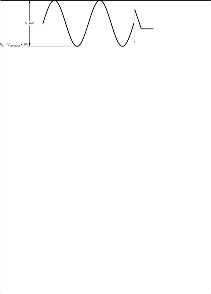
Input Test Signals
20052006
FIGURE 1. Line Transient Response Input Test Signal
20052007
FIGURE 2. PSRR Input Test Signal
www.national.com |
6 |
Typical Performance Characteristics Unless otherwise specified, CIN = COUT = 1.0 µF Ceramic, VIN = VOUT + 1.0V, TA = 25˚C, Enable pin is tied to VIN.
Output Voltage Change vs Temperature |
Ground Current vs Load Current (1.8V VOUT) |
20052011
|
20052010 |
Ground Current vs VIN @ 25˚C |
Ground Current vs VIN @125˚C |
20052014 |
20052015 |
Ground Current vs VIN @ -40˚C |
Short Circuit Current |
20052016
20052013
LP3999
7 |
www.national.com |
LP3999
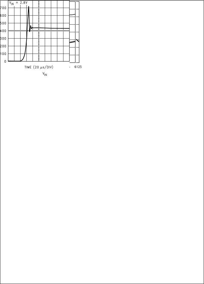
Typical Performance Characteristics Unless otherwise specified, CIN = COUT = 1.0 µF Ceramic, VIN = VOUT + 1.0V, TA = 25˚C, Enable pin is tied to VIN. (Continued)
Line Transient Response (1.8V VOUT) |
Line Transient Response (1.5V VOUT) |
20052018 |
20052017 |
Ripple Rejection (1.8V VOUT) |
Ripple Rejection (1.5V VOUT) |
20052019 |
20052020 |
Enable Start-Up Time (VOUT = 1.8V) |
Enable Start-Up Time (VOUT = 1.8V) |
20052030 |
20052031 |
www.national.com |
8 |
Typical Performance Characteristics Unless otherwise specified, CIN = COUT = 1.0 µF Ceramic, VIN = VOUT + 1.0V, TA = 25˚C, Enable pin is tied to VIN. (Continued)
Enable Start-Up Time (VOUT = 1.5V) |
Enable Start-Up Time (VOUT = 1.5V) |
20052032 |
20052033 |
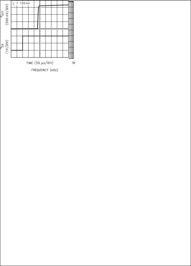
Load Transient Response (VOUT = 1.8V) |
Load Transient Response (VOUT = 1.5V) |
20052022 |
20052021 |
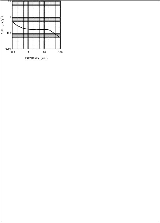
Output Noise Density VIN = 4.2V VOUT = 2.5V)
20052034
LP3999
9 |
www.national.com |

LP3999
Application Hints
POWER DISSIPATION AND DEVICE OPERATION
The permissible power dissipation for any package is a measure of the capability of the device to pass heat from the power source, the junctions of the IC, to the ultimate heat sink, the ambient environment. Thus the power dissipation is dependent on the ambient temperature and the thermal resistance across the various interfaces between the die and ambient air.
Re-stating the equation given in (Note 5) in the electrical specification section, the allowable power dissipation for the device in a given package can be calculated:
With a θJA = 255˚C/W, the device in the micro SMD package returns a value of 392 mW with a maximum junction temperature of 125˚C.
The actual power dissipation across the device can be represented by the following equation:
PD = (VIN − VOUT) x IOUT.
This establishes the relationship between the power dissipation allowed due to thermal consideration, the voltage drop across the device, and the continuous current capability of the device. These two equations should be used to determine the optimum operating conditions for the device in the application.
EXTERNAL CAPACITORS
In common with most regulators, the LP3999 requires external capacitors to ensure stable operation. The LP3999 is specifically designed for portable applications requiring minimum board space and smallest components. These capacitors must be correctly selected for good performance.
INPUT CAPACITOR
An input capacitor is required for stability. It is recommended that a 1.0 µF capacitor be connected between the LP3999 input pin and ground (this capacitance value may be increased without limit).
This capacitor must be located a distance of not more than 1 cm from the input pin and returned to a clean analogue ground. Any good quality ceramic, tantalum, or film capacitor may be used at the input.
Important: Tantalum capacitors can suffer catastrophic failures due to surge current when connected to a lowimpedance source of power (like a battery or a very large capacitor). If a tantalum capacitor is used at the input, it must be guaranteed by the manufacturer to have a surge current rating sufficient for the application.
There are no requirements for the ESR (Equivalent Series Resistance) on the input capacitor, but tolerance and temperature coefficient must be considered when selecting the capacitor to ensure the capacitance will remain 1.0 µF over the entire operating temperature range.
OUTPUT CAPACITOR
The LP3999 is designed specifically to work with very small ceramic output capacitors. A ceramic capacitor (dielectric types Z5U, Y5V or X7R) in the 1.0 [to 10 µF] range, and with ESR between 5 mΩ to 500 mΩ, is suitable in the LP3999 application circuit.
For this device the output capacitor should be connected between the VOUT pin and ground.
It may also be possible to use tantalum or film capacitors at
the device output, VOUT, but these are not as attractive for reasons of size and cost (see the section Capacitor Charac-
teristics).
The output capacitor must meet the requirement for the minimum value of capacitance and also have an ESR value that is within the range 5 mΩ to 500 mΩ for stability.
NO-LOAD STABILITY
The LP3999 will remain stable and in regulation with no external load. This is an important consideration in some circuits, for example CMOS RAM keep-alive applications.
CAPACITOR CHARACTERISTICS
The LP3999 is designed to work with ceramic capacitors on the output to take advantage of the benefits they offer. For capacitance values in the range of 1 µF to 4.7 µF, ceramic capacitors are the smallest, least expensive and have the lowest ESR values, thus making them best for eliminating high frequency noise. The ESR of a typical 1 µF ceramic capacitor is in the range of 20 mΩ to 40 mΩ, which easily meets the ESR requirement for stability for the LP3999.
The temperature performance of ceramic capacitors varies by type. Most large value ceramic capacitors ( ≥ 2.2 µF) are manufactured with Z5U or Y5V temperature characteristics, which results in the capacitance dropping by more than 50% as the temperature goes from 25˚C to 85˚C.
A better choice for temperature coefficient in a ceramic capacitor is X7R. This type of capacitor is the most stable and holds the capacitance within ±15% over the temperature range. Tantalum capacitors are less desirable than ceramic for use as output capacitors because they are more expensive when comparing equivalent capacitance and voltage ratings in the 1 µF to 4.7 µF range.
Another important consideration is that tantalum capacitors have higher ESR values than equivalent size ceramics. This means that while it may be possible to find a tantalum capacitor with an ESR value within the stable range, it would have to be larger in capacitance (which means bigger and more costly) than a ceramic capacitor with the same ESR value. It should also be noted that the ESR of a typical tantalum will increase about 2:1 as the temperature goes from 25˚C down to −40˚C, so some guard band must be allowed.
NOISE BYPASS CAPACITOR
A bypass capacitor should be connected between the CBY- PASS pin and ground to significantly reduce the noise at the regulator output. This device pin connects directly to a high impedance node within the bandgap reference circuitry. Any significant loading on this node will cause a change on the regulated output voltage. For this reason, DC leakage current through this pin must be kept as low as possible for best output voltage accuracy.
The use of a 0.01µF bypass capacitor is strongly recommended to prevent overshoot on the output during start-up.
www.national.com |
10 |