

Розрахункова СЗіВІ / Розрахункова робота / Стабілізатори напруги / LDO National Semiconductor / LP3878-ADJ
.pdfJune 1, 2009
LP3878-ADJ
Micropower 800mA Low Noise "Ceramic Stable" Adjustable Voltage Regulator for 1V to 5V Applications
General Description
The LP3878-ADJ is an 800 mA adjustable output voltage regulator designed to provide high performance and low noise in applications requiring output voltages as low as 1.0V.
Using an optimized VIP® (Vertically Integrated PNP) process, the LP3878-ADJ delivers superior performance:
Ground Pin Current: Typically 5.5 mA @ 800 mA load, and 180 µA @ 100 µA load.
Low Power Shutdown: The LP3878-ADJ draws less than 10 μA quiescent current when shutdown pin is pulled low.
Precision Output: Guaranteed output voltage accuracy is 1% at room temperature.
Low Noise: Broadband output noise is only 18 μV (typical) with 10 nF bypass capacitor.
Features
■1.0V to 5.5V output
■Designed for use with low ESR ceramic capacitors
■Very low output noise
■8 Lead PSOP and LLP surface mount package
■<10 μA quiescent current in shutdown
■Low ground pin current at all loads
■Over-temperature/over-current protection
■-40°C to +125°C operating junction temperature range
Applications
■ASIC Power Supplies In:
-Desktops, Notebooks and Graphic Cards
-Set Top Boxes, Printers and Copiers
■DSP and FPGA Power Supplies
■SMPS Post-Regulator
■Medical Instrumentation
Basic Application Circuit
20120903
*Capacitance values shown are minimum required to assure stability. Larger output capacitor provides improved dynamic response. Output capacitor must meet ESR requirements (see Application Information).
**The Shutdown pin must be actively terminated (see Application Information). Tie to INPUT (Pin 4) if not used.
VIP® is a registered trademark of National Semiconductor Corporation.
for Regulator Voltage Adjustable Stable" "Ceramic Noise Low 800mA Micropower ADJ-LP3878 Applications 5V to 1V
© 2009 National Semiconductor Corporation |
201209 |
www.national.com |

LP3878-ADJ
Connection Diagrams
8 Lead PSOP Package (MRA) |
8 Lead LLP Surface Mount Package (SD) |
20120930
Top View
See NS Package Number MRA08A
20120950
Top View
See NS Package Number SDC08A
Ordering Information
TABLE 1. Package Marking and Ordering Information
Output Voltage |
Grade |
Order Information |
Supplied as: |
ADJ |
STD |
LP3878MR-ADJ |
95 Units per Rail |
|
|
|
|
ADJ |
STD |
LP3878MRX-ADJ |
2500 Units on Tape and Reel |
ADJ |
STD |
LP3878SD-ADJ |
1000 Units on Tape and Reel |
|
|
|
|
ADJ |
STD |
LP3878SDX-ADJ |
4500 Units on Tape and Reel |
|
|
|
|
Pin Descriptions
Pin |
Name |
Function |
1 |
BYPASS |
The capacitor connected between BYPASS and GROUND lowers output |
|
|
noise voltage level and is required for loop stability. |
2 |
N/C |
DO NOT CONNECT. This pin is used for post package test and must be |
|
|
left floating. |
|
|
|
3 |
GROUND |
Device ground. |
|
|
|
4 |
INPUT |
Input source voltage. |
5 |
OUTPUT |
Regulated output voltage. |
|
|
|
6 |
ADJ |
Provides feedback to error amplifier from the resistive divider that sets the |
|
|
output voltage. |
|
|
|
7 |
N/C |
No internal connection. |
|
|
|
8 |
SHUTDOWN |
Output is enabled above turn-on threshold voltage. Pull down to turn off |
|
|
regulator output. |
|
|
|
PSOP, LLP |
SUBSTRATE |
The exposed die attach pad should be connected to a thermal pad at |
DAP |
GROUND |
ground potential. For additional information on using National |
|
|
Semiconductor's Non Pull Back LLP package, please refer to LLP |
|
|
application note AN-1187 |
|
|
|
www.national.com |
2 |
Absolute Maximum Ratings (Note 1)
If Military/Aerospace specified devices are required, please contact the National Semiconductor Sales Office/ Distributors for availability and specifications.
Storage Temperature Range |
−65°C to +150°C |
|
Operating Junction |
Temperature |
|
Range |
|
-40°C to +125°C |
Lead Temperature |
(Soldering, 5 |
|
seconds) |
|
260°C |
ESD Rating (Note 2) |
|
2 kV |
Shutdown Pin |
|
1kV |
Power Dissipation (Note 3) |
Internally Limited |
Input Supply Voltage (Survival) |
−0.3V to +16V |
Input Supply Voltage (Typical |
|
Operating) |
2.5V to +16V |
ADJ Pin |
−0.3V to +6V |
Output Voltage (Survival) (Note 4) |
−0.3V to +6V |
IOUT (Survival) |
Short Circuit |
|
Protected |
Input-Output Voltage (Survival) |
|
(Note 5) |
−0.3V to +16V |
Electrical Characteristics
Limits in standard typeface are for TJ = 25°C, and limits in boldface type apply over the temperature range of -40°C to 125°C. Limits are guaranteed through design, testing, or correlation. The limits are used to calculate National's Average Outgoing Quality
Level (AOQL). Unless otherwise specified: VIN = 3.0V, VOUT = 1V, IL = 1 mA, COUT = 10 µF, CIN = 4.7 µF, VS/D = 2V, CBYPASS = 10 nF.
Symbol |
Parameter |
Conditions |
Min |
Typical |
Max |
Units |
VADJ |
Adjust Pin Voltage |
|
0.99 |
1.00 |
1.01 |
|
|
|
1 mA ≤ IL ≤ 800 mA |
0.98 |
1.00 |
1.02 |
V |
|
|
3.0V ≤ VIN ≤ 6V |
0.97 |
1.03 |
|
|
|
|
|
|
|||
|
Output Voltage Line |
3.0V ≤ VIN ≤ 16V |
|
0.007 |
0.014 |
%/V |
|
Regulation |
|
|
0.032 |
||
|
|
|
|
|
||
|
|
|
|
|
|
|
|
|
IL = 800 mA |
|
2.5 |
3.1 |
|
|
|
VOUT ≥ VOUT(NOM) - 1% |
|
|
||
|
|
|
|
|
|
|
|
Minimum Input Voltage |
IL = 800 mA |
|
|
|
|
VIN (min) |
Required To Maintain |
VOUT ≥ VOUT(NOM) - 1% |
|
2.5 |
2.8 |
V |
|
Output Regulation |
0 ≤ TJ ≤ 125°C |
|
|
|
|
|
|
IL = 750 mA |
|
2.5 |
3.0 |
|
|
|
VOUT ≥ VOUT(NOM) - 1% |
|
|
||
|
|
|
|
|
|
|
|
|
IL = 100 µA |
|
1 |
2 |
|
|
|
|
|
|
3 |
|
VDO |
Dropout Voltage (Note 6) |
IL = 200 mA |
|
150 |
200 |
mV |
VOUT = 3.8V |
|
|
|
300 |
||
|
|
|
|
|
||
|
|
IL = 800 mA |
|
475 |
600 |
|
|
|
|
|
|
1100 |
|
|
|
|
|
|
|
|
IGND |
Ground Pin Current |
IL = 100 µA |
|
180 |
200 |
µA |
|
|
|
|
225 |
||
|
|
|
|
|
|
|
|
|
IL = 200 mA |
|
1.5 |
2 |
|
|
|
|
|
3.5 |
|
|
|
|
|
|
|
mA |
|
|
|
IL = 800 mA |
|
5.5 |
8.5 |
|
|
|
|
|
|||
|
|
|
|
15 |
|
|
|
|
|
|
|
|
|
|
|
|
|
|
|
|
IO(PK) |
Peak Output Current |
VOUT ≥ VOUT(NOM) − 5% |
|
1200 |
|
mA |
IO(MAX) |
Short Circuit Current |
RL = 0 (Steady State) |
|
1300 |
|
|
|
|
|
||||
en |
Output Noise Voltage |
BW = 100 Hz to 100 kHz |
|
18 |
|
µV(RMS) |
|
(RMS) |
CBYPASS = 10 nF |
|
|
||
|
|
|
|
|
||
|
Ripple Rejection |
f = 1 kHz |
|
60 |
|
dB |
|
|
|
|
|
||
|
|
|
|
|
|
|
IADJ |
ADJ Pin Bias Current |
IL = 800 mA |
|
200 |
|
nA |
|
(Sourcing) |
|
|
|
||
|
|
|
|
|
|
|
|
|
|
|
|
|
|
ADJ-LP3878
3 |
www.national.com |

ADJ |
|
|
|
|
|
|
|
|
|
Symbol |
Parameter |
Conditions |
Min |
Typical |
Max |
Units |
|
||
- |
|
|
|
|
|
|
|
|
|
|
|
VL = Output OFF |
|
|
|
|
|
||
LP3878 |
SHUTDOWN INPUT |
|
|
|
|
|
|||
|
|
|
|
|
|
|
|
||
|
|
|
|
|
|
|
|
|
|
|
|
VS/D |
S/D Input Voltage |
VH = Output ON |
|
1.4 |
1.6 |
|
|
|
|
|
|
IIN ≤ 10 µA |
0.04 |
0.20 |
|
V |
|
|
|
|
|
|
|
|
|
||
|
|
|
|
VOUT ≤ 10 mV |
|
0.6 |
|
|
|
|
|
|
|
IIN ≤ 50 µA |
|
|
|
|
|
|
|
|
|
|
|
|
|
|
|
|
|
IS/D |
S/D Input Current |
VS/D = 0 |
|
0.02 |
−1 |
µA |
|
|
|
|
|
VS/D = 5V |
|
5 |
15 |
|
|
|
|
|
|
|
|
|
|||
Note 1: Absolute Maximum Ratings indicate limits beyond which damage to the component may occur. Electrical specifications do not apply when operating the device outside of its rated operating conditions.
Note 2: ESD testing was performed using Human Body Model, a 100 pF capacitor discharged through a 1.5 kΩ resistor.
Note 3: The maximum allowable power dissipation is a function of the maximum junction temperature, TJ(MAX), the junction-to-ambient thermal resistance, θJ −A, and the ambient temperature, TA. The maximum allowable power dissipation at any ambient temperature is calculated using:
The value of θJ−A for the LLP (SD) and PSOP (MRA) packages are specifically dependent on PCB trace area, trace material, and the number of layers and thermal vias. If a four layer board is used with maximum vias from the IC center to the heat dissipating copper layers, values of θJ−A which can be obtained are approximately 60°C/W for the PSOP-8 and 40°C/W for the LLP-8 package. For improved thermal resistance and power dissipation for the LLP package, refer to Application Note AN-1187. Exceeding the maximum allowable power dissipation will cause excessive die temperature, and the regulator will go into thermal shutdown.
Note 4: If used in a dual-supply system where the regulator load is returned to a negative supply, the LP3878-ADJ output must be diode-clamped to ground.
Note 5: The output PNP structure contains a diode between the VIN and VOUT terminals that is normally reverse-biased. Forcing the output above the input will turn on this diode and may induce a latch-up mode which can damage the part (see Application Hints).
Note 6: Dropout voltage spec applies only if VIN is sufficient so that it does not limit regulator operation.
www.national.com |
4 |
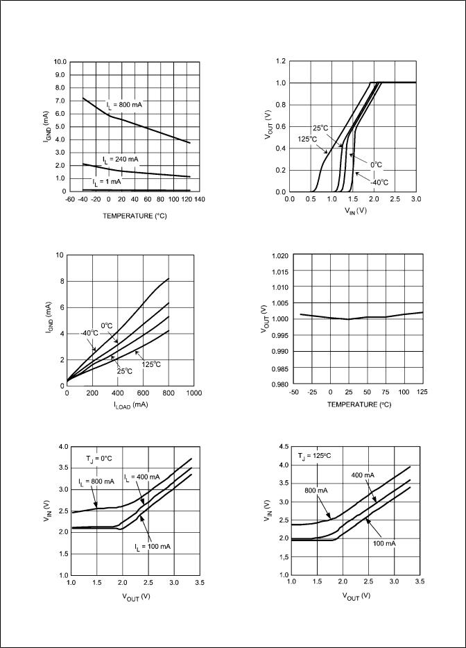
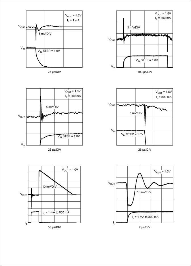
Typical Performance Characteristics |
Unless otherwise specified: VIN = 3.3V, VOUT = 1V, IL = 1 mA, |
CIN = 4.7 µF, COUT = 10 µF, VS/D = 2V, CBYP = 10 nF, TJ = 25°C. |
|
IGND vs Temperature |
Minimum VIN Over Temperature |
|
20120921 |
|
20120920 |
IGND vs ILoad |
VOUT vs Temperature |
|
20120922 |
20120959 |
|
|
|
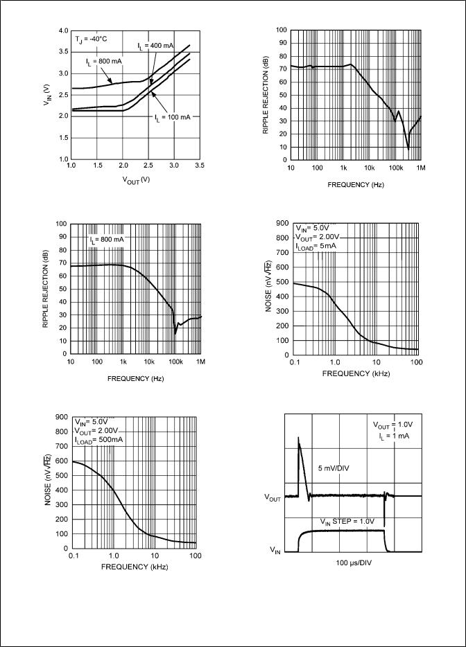
Minimum VIN vs VOUT |
|
Minimum VIN vs VOUT |
20120951 |
20120952 |
ADJ-LP3878
5 |
www.national.com |
LP3878-ADJ
Minimum VIN vs VOUT |
Ripple Rejection |
20120953
20120954
Ripple Rejection |
Output Noise Spectral Density |
20120947
|
20120958 |
Output Noise Spectral Density |
Line Transient Response |
20120931
20120948
www.national.com |
6 |
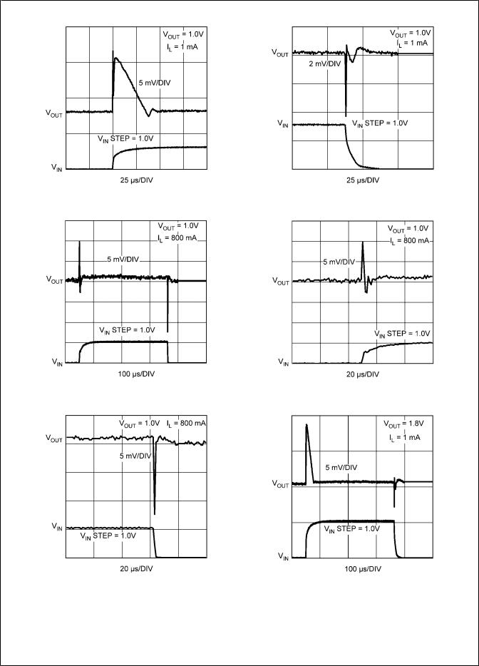
Line Transient Response |
Line Transient Response |
20120933 20120932
Line Transient Response Line Transient Response
20120935 20120936
Line Transient Response Line Transient Response
20120934 |
20120937 |
ADJ-LP3878
7 |
www.national.com |
LP3878-ADJ
Line Transient Response |
Line Transient Response |
20120939 20120940
Line Transient Response Line Transient Response
20120942 20120941
Load Transient Response Load Transient Response
20120945 |
20120943 |
www.national.com |
8 |
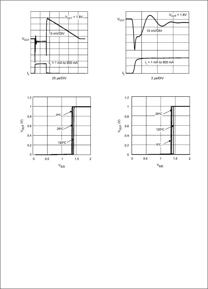
Load Transient Response |
Load Transient Response |
20120946 20120944
Turn-On Characteristics Turn-Off Characteristics
20120955 |
20120956 |
ADJ-LP3878
9 |
www.national.com |
LP3878-ADJ
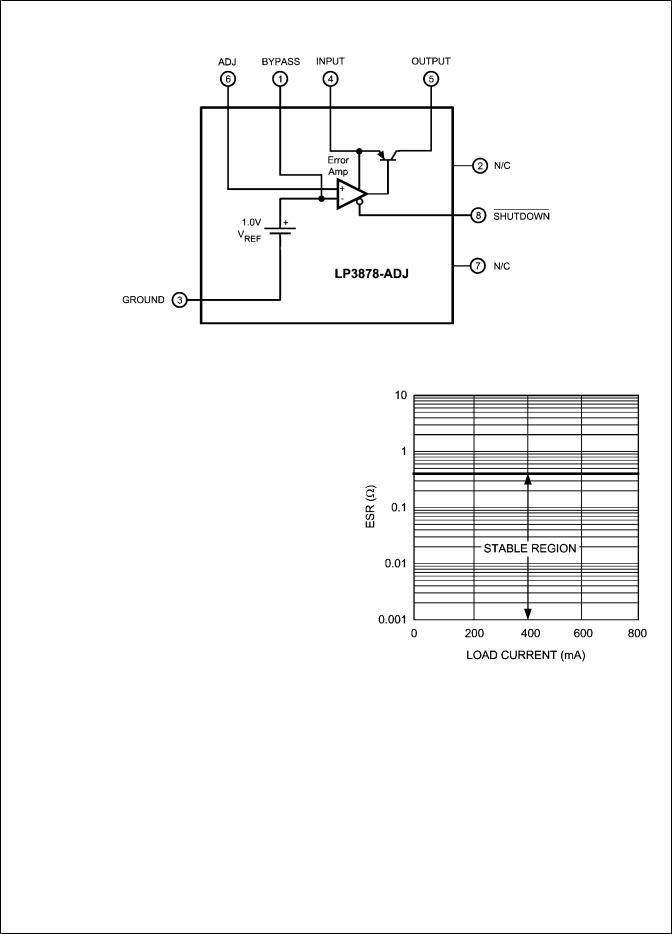
Block Diagram
Application Information
PACKAGE INFORMATION
The LP3878-ADJ is offered in the 8 lead PSOP or LLP surface mount packages to allow for increased power dissipation compared to the SO-8 and Mini SO-8. For details on thermal performance as well as mounting and soldering specifications, refer to Application Note AN-1187.
EXTERNAL CAPACITORS
Like any low-dropout regulator, the LP3878-ADJ requires external capacitors for regulator stability. These capacitors must be correctly selected for good performance.
INPUT CAPACITOR: A capacitor whose value is at least 4.7 µF (±20%) is required between the LP3878-ADJ input and ground. A good quality X5R / X7R ceramic capacitor should be used.
Capacitor tolerance and temperature variation must be considered when selecting a capacitor (see Capacitor Characteristics section) to assure the minimum requirement of input capacitance is met over all operating conditions.
The input capacitor must be located not more than 0.5" from the input pin and returned to a clean analog ground. Any good quality ceramic or tantalum capacitor may be used, assuming the minimum input capacitance requirement is met.
OUTPUT CAPACITOR: The LP3878-ADJ requires a ceramic output capacitor whose size is at least 10 µF (±20%). A good quality X5R / X7R ceramic capacitor should be used. Capacitance tolerance and temperature characteristics must be considered when selecting an output capacitor.
The LP3878-ADJ is designed specifically to work with ceramic output capacitors, utilizing circuitry which allows the regulator to be stable across the entire range of output current with an ultra low ESR output capacitor.
The output capacitor selected must meet the requirement for minimum amount of capacitance and also have an ESR (equivalent series resistance) value which is within the stable range. A curve is provided which shows the stable ESR range as a function of load current (see Figure 1).
20120901
20120938
FIGURE 1. Stable Region For Output Capacitor ESR
Important: The output capacitor must maintain its ESR within the stable region over the full operating temperature range of the application to assure stability.
The output capacitor ESR forms a zero which is required to add phase lead near the loop gain crossover frequency, typically in the range of 50kHz to 200 kHz. The ESR at lower frequencies is of no importance. Some capacitor manufacturers list ESR at low frequencies only, and some give a formula for Dissipation Factor which can be used to calculate a value for a term referred to as ESR. However, since the DF formula is usually at a much lower frequency than the range listed above, it will give an unrealistically high value. If good quality X5R or X7R ceramic capacitors are used, the actual ESR in the 50 kHz to 200 kHz range will not exceed 25 milli
www.national.com |
10 |