
Розрахункова СЗіВІ / Розрахункова робота / Стабілізатори напруги / LDO National Semiconductor / LP38858
.pdf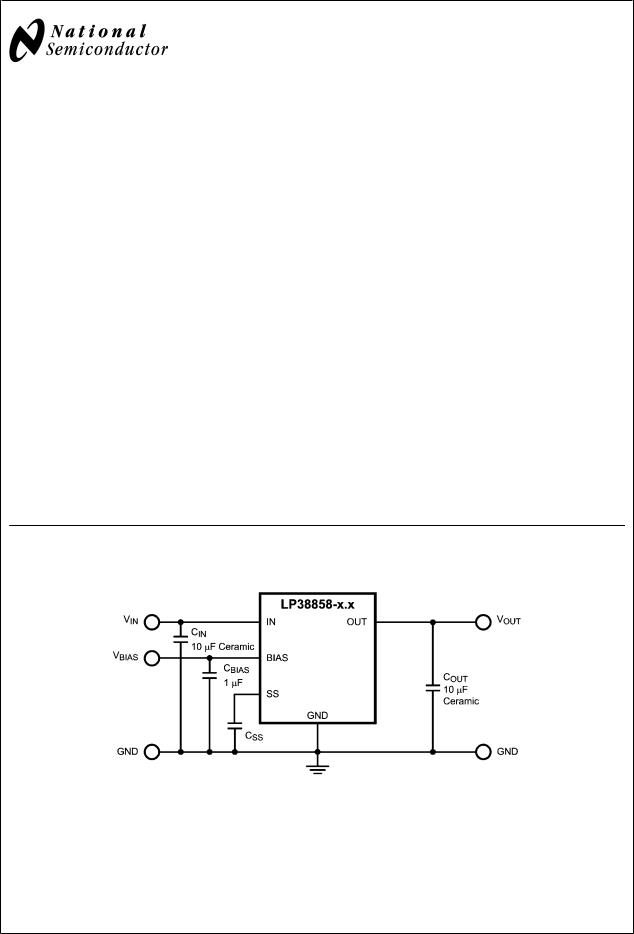
November 2006
LP38858
1.5A Fast-Response High-Accuracy LDO Linear Regulator with Soft-Start
General Description
The LP38858 is a high current, fast response regulator which can maintain output voltage regulation with extremely low input to output voltage drop. Fabricated on a CMOS process, the device operates from two input voltages: VBIAS provides voltage to drive the gate of the N-MOS power transistor, while VIN is the input voltage which supplies power to the load. The use of an external bias rail allows the part to operate from ultra low VIN voltages. Unlike bipolar regulators, the CMOS architecture consumes extremely low quiescent current at any output load current. The use of an N-MOS power transistor results in wide bandwidth, yet minimum external capacitance is required to maintain loop stability.
The fast transient response of this device makes it suitable for use in powering DSP, Microcontroller Core voltages and Switch Mode Power Supply post regulators. The LP38858 is available in TO-220 and TO-263 5-Lead packages.
Dropout Voltage: 130mV (typical) at 1.5A load current.
Low Ground Pin Current: 14 mA (typical) at 1.5A load current.
Soft-Start: Programmable Soft-Start time.
Precision Output Voltage: ±1.0% for TJ = 25°C and ±2.0% for 0°C ≤ TJ ≤ +125°C, across all line and load conditions
Features
■Standard VOUT values of 0.8V and 1.2V
■Wide VBIAS Supply operating range of 3.0V to 5.5V
■Stable with 10µF Ceramic capacitors
■Dropout voltage of 130 mV (typical) at 1.5A load current
■Precision Output Voltage across all line and load conditions:
—±1.0% VOUT for TJ = 25°C
—±2.0% VOUT for 0°C ≤ TJ ≤ +125°C
—±3.0% VOUT for -40°C ≤ TJ ≤ +125°C
■Over-Temperature and Over-Current protection
■Available in 5 lead TO-220 and TO-263 packages
■Custom VOUT values between 0.8V and 1.2V are available
■−40°C to +125°C Operating Temperature Range
Applications
■ASIC Power Supplies In:
-Desktops, Notebooks, and Graphics Cards, Servers
-Gaming Set Top Boxes, Printers and Copiers
■Server Core and I/O Supplies
■DSP and FPGA Power Supplies
■SMPS Post-Regulator
Typical Application Circuit
20202701
Start-Soft with Regulator Linear LDO Accuracy-High Response-Fast 5A.1 LP38858
© 2007 National Semiconductor Corporation |
202027 |
www.national.com |
LP38858
Ordering Information
VOUT * |
Order Number |
Package Type |
Package Drawing |
Supplied As |
|
LP38858S-0.8 |
TO263-5 |
TS5B |
Rail of 45 |
|
|
|
|
|
0.8V |
LP38858SX-0.8 |
TO263-5 |
TS5B |
Tape and Reel of 500 |
|
|
|
|
|
|
LP38858T-0.8 |
TO220-5 |
T05D |
Rail of 45 |
|
LP38858S-1.2 |
TO263-5 |
TS5B |
Rail of 45 |
|
|
|
|
|
1.2V |
LP38858SX-1.2 |
TO263-5 |
TS5B |
Tape and Reel of 500 |
|
|
|
|
|
|
LP38858T-1.2 |
TO220-5 |
T05D |
Rail of 45 |
* For custom VOUT values between 0.8V and 1.2V please contact the National Semiconductor Sales Office.
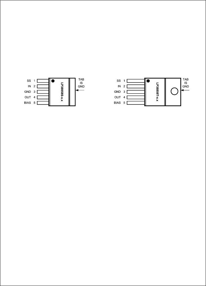
Connection Diagrams
|
|
|
20202702 |
20202703 |
|
|
TO263–5, Top View |
|
TO220–5, Top View |
|
|
Pin Descriptions |
|
|
|
||
|
|
|
TO220–5 and TO263–5 Packages |
|
|
|
|
|
|
|
|
Pin # |
|
Pin Symbol |
|
Pin Description |
|
1 |
|
SS |
|
Soft-Start capacitor connection. Used to slow the rise time of VOUT at turn-on. |
|
2 |
|
IN |
|
The unregulated voltage input pin. |
|
3 |
|
GND |
|
Ground |
|
|
|
|
|
|
|
4 |
|
OUT |
|
The regulated output voltage pin. |
|
|
|
|
|
|
|
5 |
|
BIAS |
|
The supply for the internal control and reference circuitry. |
|
|
|
|
|
The TAB is a thermal connection that is physically attached to the backside of |
|
TAB |
|
TAB |
|
the die, and used as a thermal heat-sink connection. See the Application |
|
|
|
|
|
Information section for details. |
|
|
|
|
|
|
|
www.national.com |
2 |

Absolute Maximum Ratings (Note 1)
If Military/Aerospace specified devices are required, please contact the National Semiconductor Sales Office/ Distributors for availability and specifications.
Storage Temperature Range |
−65°C to +150°C |
Lead Temperature |
|
Soldering, 5 seconds |
260°C |
ESD Rating |
|
Human Body Model (Note 2) |
±2 kV |
Power Dissipation (Note 3) |
Internally Limited |
VIN Supply Voltage (Survival) |
−0.3V to +6.0V |
VBIAS Supply Voltage (Survival) |
−0.3V to +6.0V |
VSS Soft-Start Voltage (Survival) |
−0.3V to +6.0V |
VOUT Voltage (Survival) |
−0.3V to +6.0V |
IOUT Current (Survival) |
Internally Limited |
Junction Temperature |
−40°C to +150°C |
Operating Ratings (Note 1)
VIN Supply Voltage |
(VOUT + VDO) to VBIAS |
VBIAS Supply Voltage |
3.0V to 5.5V |
IOUT |
0 mA to 1.5A |
Junction Temperature Range |
−40°C to +125°C |
(Note 3) |
|
Electrical Characteristics Unless otherwise specified: VIN = VOUT(NOM) + 1V, VBIAS = 3.0V, IOUT = 10 mA, CIN = COUT = 10 µF, CBIAS = 1 µF, CSS = open. Limits in standard type are for TJ = 25°C only; limits in boldface type apply over the junction temperature (TJ) range of -40°C to +125°C. Minimum and Maximum limits are guaranteed through test, design, or statistical
correlation. Typical values represent the most likely parametric norm at TJ = 25°C, and are provided for reference purposes only.
Symbol |
Parameter |
Conditions |
MIN |
TYP |
MAX |
Units |
|
|
|
VOUT(NOM) + 1V ≤ VIN ≤ VBIAS, |
-1.0 |
|
1.0 |
|
|
|
|
3.0V ≤ VBIAS ≤ 5.5V, |
0 |
|
|||
|
|
-3.0 |
3.0 |
|
|||
|
|
10 mA ≤ IOUT ≤ 1.5A |
|
|
|||
|
|
|
|
|
|
||
VOUT |
VOUT Accuracy |
VOUT(NOM) + 1V ≤ VIN ≤ VBIAS, |
|
|
|
% |
|
|
|
3.0V ≤ VBIAS ≤ 5.5V, |
-2.0 |
0 |
2.0 |
|
|
|
|
10 mA ≤ IOUT ≤ 1.5A, |
|
||||
|
|
|
|
|
|
||
|
|
0°C ≤ TJ ≤ +125°C |
|
|
|
|
|
VOUT/ΔVIN |
Line Regulation, VIN |
VOUT(NOM) + 1V ≤ VIN ≤ VBIAS |
- |
0.04 |
- |
%/V |
|
(Note 4) |
|||||||
|
|
|
|
|
|
||
|
|
|
|
|
|
|
|
VOUT/ΔVBIAS |
Line Regulation, VBIAS |
3.0V ≤ VBIAS ≤ 5.5V |
- |
0.10 |
- |
%/V |
|
(Note 4) |
|||||||
|
|
|
|
|
|
||
|
|
|
|
|
|
|
|
VOUT/ΔIOUT |
Output Voltage Load Regulation |
10 mA ≤ IOUT ≤ 1.5A |
- |
0.2 |
- |
%/A |
|
(Note 5) |
|||||||
|
|
|
|
|
|
||
|
|
|
|
|
|
|
|
VDO |
Dropout Voltage (Note 6) |
IOUT = 1.5A |
- |
130 |
165 |
mV |
|
180 |
|||||||
|
|
|
|
|
|
||
|
|
LP38858-0.8 |
- |
7.0 |
8.5 |
|
|
|
Quiescent Current Drawn from |
10 mA ≤ IOUT ≤ 1.5A |
9.0 |
|
|||
IGND(IN) |
|
|
mA |
||||
VIN Supply |
LP38858-1.2 |
|
11 |
12 |
|||
|
|
|
|||||
|
|
10 mA ≤ IOUT ≤ 1.5A |
|
15 |
|
||
|
|
|
|
|
|||
IGND(BIAS) |
Quiescent Current Drawn from |
10 mA ≤ IOUT ≤ 1.5A |
- |
3.0 |
3.8 |
mA |
|
VBIAS Supply |
4.5 |
||||||
|
|
|
|
|
|||
UVLO |
Under-Voltage Lock-Out |
VBIAS rising until device is |
2.20 |
2.45 |
2.70 |
V |
|
Threshold |
functional |
2.00 |
2.90 |
||||
|
|
|
|||||
|
|
|
|
|
|
|
|
UVLO(HYS) |
Under-Voltage Lock-Out |
VBIAS falling from UVLO threshold |
60 |
150 |
300 |
mV |
|
Hysteresis |
until device is non-functional |
50 |
350 |
||||
|
|
|
|||||
|
|
|
|
|
|
|
|
ISC |
Output Short-Circuit Current |
VIN = VOUT(NOM) + 1V, |
- |
4.5 |
- |
A |
|
VBIAS = 3.0V, VOUT = 0.0V |
|||||||
|
|
|
|
|
|
||
Soft-Start |
|
|
|
|
|
|
|
rSS |
Soft-Start internal resistance |
LP38858-0.8 |
11.0 |
13.5 |
16.0 |
kΩ |
|
|
|
|
|
||||
LP38858-1.2 |
13.5 |
16.0 |
18.5 |
||||
|
|
|
|||||
|
|
|
|
|
|
|
|
tSS |
Soft-Start time |
LP38858-0.8, CSS = 10 nF |
- |
675 |
- |
μs |
|
tSS = CSS × rSS × 5 |
LP38858-1.2, CSS = 10 nF |
- |
800 |
- |
|||
|
|
LP38858
3 |
www.national.com |

LP38858 |
|
|
|
|
|
|
|
|
|
|
|
Symbol |
Parameter |
Conditions |
MIN |
TYP |
MAX |
Units |
|
||||
|
|
|
|||||||||
|
|
AC Parameters |
|
|
|
|
|
|
|
|
|
|
|
|
|
|
|
|
|
|
|
|
|
|
|
|
|
VIN = VOUT(NOM) + 1V, |
- |
80 |
- |
|
|
|
|
|
|
PSRR |
Ripple Rejection for VIN Input |
f = 120 Hz |
|
|
|
|
|||
|
|
|
|
|
|
|
|
|
|||
|
|
(VIN) |
Voltage |
VIN = VOUT(NOM) + 1V, |
- |
65 |
- |
|
|
|
|
|
|
|
|
f = 1 kHz |
|
|
|
|
|||
|
|
|
|
|
|
|
dB |
|
|||
|
|
|
|
|
|
|
|
|
|||
|
|
|
|
VBIAS = VOUT(NOM) + 3V, |
- |
58 |
- |
|
|||
|
|
|
|
|
|
|
|
||||
|
|
PSRR |
|
f = 120 Hz |
|
|
|
|
|||
|
|
Ripple Rejection for VBIAS Voltage |
|
|
|
|
|
|
|
||
|
|
(VBIAS) |
VBIAS = VOUT(NOM) + 3V, |
- |
58 |
- |
|
|
|
|
|
|
|
|
|
|
|
|
|||||
|
|
|
|
f = 1 kHz |
|
|
|
|
|||
|
|
|
|
|
|
|
|
|
|
|
|
|
|
|
Output Noise Density |
f = 120 Hz |
- |
1 |
- |
µV/√ |
|
|
|
|
|
|
Hz |
|
|||||||
|
|
en |
Output Noise Voltage |
BW = 10 Hz − 100 kHz |
- |
150 |
- |
µVRMS |
|
||
|
|
|
VOUT = 1.8V |
BW = 300 Hz − 300 kHz |
- |
90 |
- |
|
|||
|
|
|
|
|
|
|
|||||
|
|
Thermal Parameters |
|
|
|
|
|
|
|
|
|
|
|
TSD |
Thermal Shutdown Junction |
|
- |
160 |
- |
|
|
|
|
|
|
Temperature |
|
°C |
|
||||||
|
|
|
|
|
|
|
|
||||
|
|
TSD(HYS) |
Thermal Shutdown Hysteresis |
|
- |
10 |
- |
|
|
|
|
|
|
θJ-A |
Thermal Resistance, Junction to |
TO220-5 |
- |
60 |
- |
|
|
|
|
|
|
Ambient(Note 3) |
TO263-5 |
- |
60 |
- |
°C/W |
|
|||
|
|
|
|
||||||||
|
|
|
|
|
|
|
|
|
|||
|
|
θJ-C |
Thermal Resistance, Junction to |
TO220-5 |
- |
3 |
- |
|
|||
|
|
|
|
|
|
||||||
|
|
Case(Note 3) |
TO263-5 |
- |
3 |
- |
|
|
|
|
|
|
|
|
|
|
|
|
|||||
Note 1: Note 1: Absolute Maximum Ratings indicate limits beyond which damage to the device may occur. Operating Ratings indicate conditions for which the device is intended to be functional, but does not guarantee specific performance limits. For guaranteed specifications and conditions, see the Electrical Characteristics.
Note 2: The human body model is a 100 pF capacitor discharged through a 1.5k resistor into each pin. Test method is per JESD22-A114. The HBM rating for device pin 1 (SS) is ±1.5 kV.
Note 3: Device power dissipation must be de-rated based on device power dissipation (PD), ambient temperature (TA), and package junction to ambient thermal resistance (θJA). Additional heat-sinking may be required to ensure that the device junction temperature (TJ) does not exceed the maximum operating rating. See the Application Information section for details.
Note 4: Output voltage line regulation is defined as the change in output voltage from nominal value resulting from a change in input voltage.
Note 5: Output voltage load regulation is defined as the change in output voltage from nominal value as the load current increases from no load to full load.
Note 6: Dropout voltage is defined the as input to output voltage differential (VIN - VOUT) where the input voltage is low enough to cause the output voltage to drop 2% from the nominal value.
www.national.com |
4 |
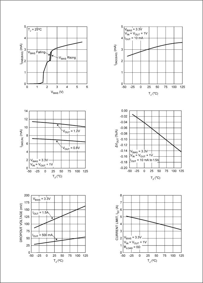
Typical Performance Characteristics Unless otherwise specified: TJ = 25°C, VIN = VOUT(NOM) + 1V, VBIAS = 3.0V, IOUT = 10 mA, CIN = COUT = 10 µF Ceramic, CBIAS = 1 µF Ceramic, CSS = open.
VBIAS Ground Pin Current (IGND(BIAS)) vs VBIAS |
VBIAS Ground Pin Current (IGND(BIAS)) vs Temperature |
20202787 |
20202761 |
|
|
VIN Ground Pin Current vs Temperature |
Load Regulation vs Temperature |
20202762 |
20202763 |
|
|
Dropout Voltage (VDO) vs Temperature |
Output Current Limit (ISC) vs Temperature |
20202765 |
20202766 |
LP38858
5 |
www.national.com |
LP38858
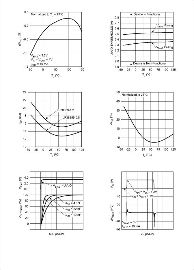
VOUT vs Temperature |
UVLO Thresholds vs Temperature |
20202767 |
20202768 |
|
|
Soft-Start Resistor (rSS) vs Temperature |
Soft-Start rSS Variation vs Temperature |
20202774 |
20202775 |
VOUT vs CSS, 10 nF to 47 nF |
VIN Line Transient Response |
20202776 |
20202777 |
www.national.com |
6 |
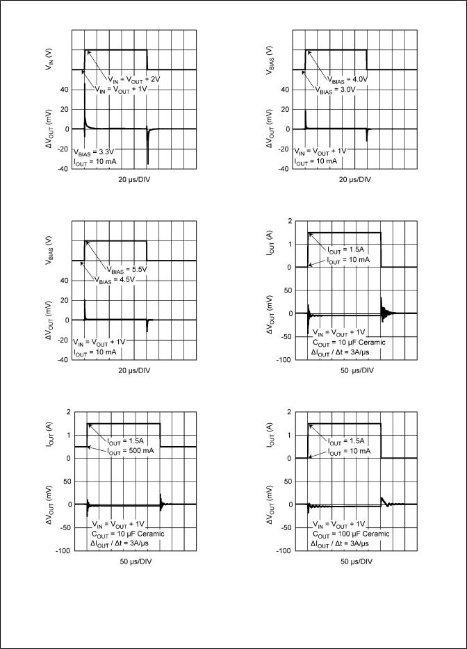
VIN Line Transient Response |
VBIAS Line Transient Response |
20202778 |
20202779 |
VBIAS Line Transient Response |
Load Transient Response, COUT = 10 µF Ceramic |
20202780 |
20202781 |
Load Transient Response, COUT = 10 µF Ceramic |
Load Transient Response, COUT = 100 µF Ceramic |
20202782 |
20202783 |
LP38858
7 |
www.national.com |
LP38858
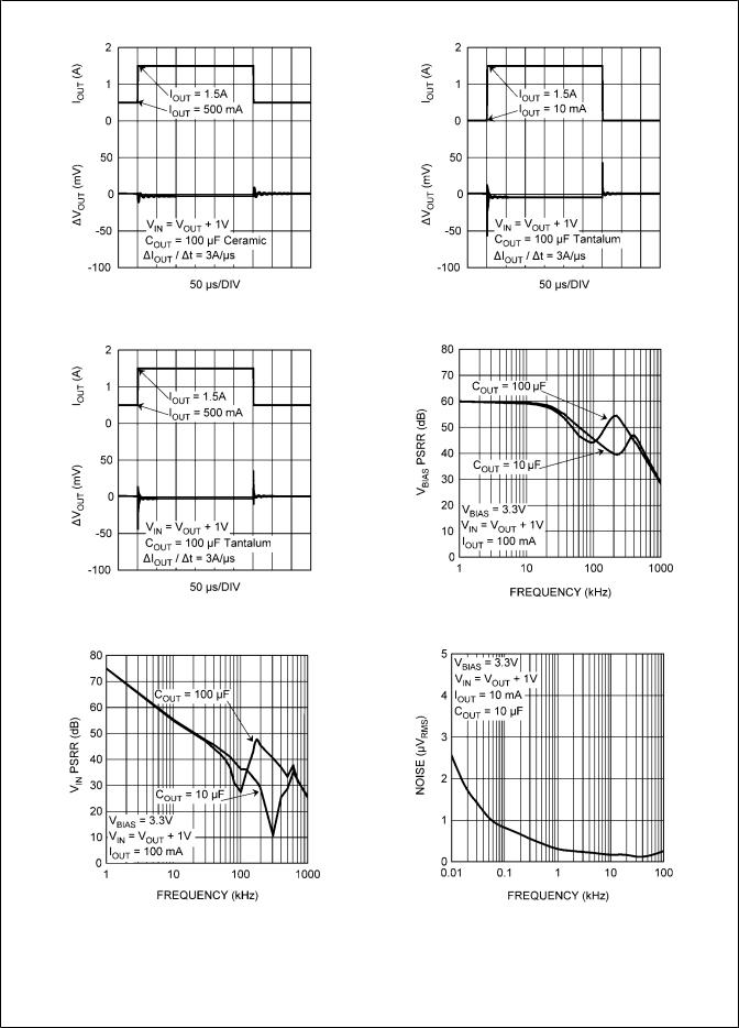
Load Transient Response, COUT = 100 µF Ceramic |
Load Transient Response, COUT = 100 µF Tantalum |
20202784 |
20202785 |
Load Transient Response, COUT = 100 µF Tantalum |
VBIAS PSRR |
|
20202786 |
20202770 |
|
|
|
VIN PSRR |
|
Output Noise |
20202771 |
20202769 |
www.national.com |
8 |
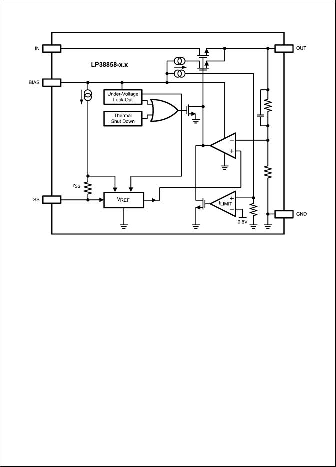
Block Diagram
LP38858
20202705
9 |
www.national.com |

LP38858
Application Information
EXTERNAL CAPACITORS
To assure regulator stability, input and output capacitors are required as shown in the Typical Application Circuit.
Output Capacitor
A minimum output capacitance of 10 µF, ceramic, is required for stability. The amount of output capacitance can be increased without limit. The output capacitor must be located less than 1 cm from the output pin of the IC and returned to the device ground pin with a clean analog ground.
Only high quality ceramic types such as X5R or X7R should be used, as the Z5U and Y5F types do not provide sufficient capacitance over temperature.
Tantalum capacitors will also provide stable operation across the entire operating temperature range. However, the effects of ESR may provide variations in the output voltage during fast load transients. Using the minimum recommended 10 µF ceramic capacitor at the output will allow unlimited capacitance, Tantalum and/or Aluminum, to be added in parallel.
Input Capacitor
The input capacitor must be at least 10 µF, but can be increased without limit. It's purpose is to provide a low source impedance for the regulator input. A ceramic capacitor, X5R or X7R, is recommended.
Tantalum capacitors may also be used at the input pin. There is no specific ESR limitation on the input capacitor (the lower, the better).
Aluminum electrolytic capacitors can be used, but are not recommended as their ESR increases very quickly at cold temperatures. They are not recommended for any application where the ambient temperature falls below 0°C.
Bias Capacitor
The capacitor on the bias pin must be at least 1 µF, and can be any good quality capacitor (ceramic is recommended).
INPUT VOLTAGE
The input voltage (VIN) is the high current external voltage rail that will be regulated down to a lower voltage, which is applied
to the load. The input voltage must be at least VOUT + VDO, and no higher than whatever values is used for VBIAS.
BIAS VOLTAGE
The bias voltage (VBIAS) is a low current external voltage rail required to bias the control circuitry and provide gate drive for
the N-FET pass transistor. The bias voltage must be in the range of 3.0V to 5.5V to ensure proper operation of the device.
UNDER VOLTAGE LOCKOUT
The bias voltage is monitored by a circuit which prevents the device from functioning when the bias voltage is below the Under-Voltage Lock-Out (UVLO) threshold of approximately 2.45V.
As the bias voltage rises above the UVLO threshold the device control circuitry becomes active. There is approximately 150 mV of hysteresis built into the UVLO threshold to provide noise immunity.
When the bias voltage is between the UVLO threshold and the Minimum Operating Rating value of 3.0V the device will be functional, but the operating parameters will not be within the guaranteed limits.
SUPPLY SEQUENCING
There is no requirement for the order that VIN or VBIAS are applied or removed.
One practical limitation is that the Soft-Start circuit starts charging CSS when VBIAS rises above the UVLO threshold. If the application of VIN is delayed beyond this point the benefits of Soft-Start will be compromised.
In any case, the output voltage cannot be guaranteed until
both VIN and VBIAS are within the range of guaranteed operating values.
If used in a dual-supply system where the regulator output load is returned to a negative supply, the output pin must be diode clamped to ground. A Schottky diode is recommended for this diode clamp.
REVERSE VOLTAGE
A reverse voltage condition will exist when the voltage at the output pin is higher than the voltage at the input pin. Typically this will happen when VIN is abruptly taken low and COUT continues to hold a sufficient charge such that the input to output voltage becomes reversed.
The NMOS pass element, by design, contains no body diode. This means that, as long as the gate of the pass element is not driven, there will not be any reverse current flow through the pass element during a reverse voltage event. The gate of
the pass element is not driven when VBIAS is below the UVLO threshold.
When VBIAS is above the UVLO threshold the control circuitry is active and will attempt to regulate the output voltage. Since
the input voltage is less than the output voltage the control
circuit will drive the gate of the pass element to the full VBIAS potential when the output voltage begins to fall. In this condi-
tion, reverse current will flow from the output pin to the input
pin , limited only by the RDS(ON) of the pass element and the output to input voltage differential. Discharging an output ca-
pacitor up to 1000 μF in this manner will not damage the device as the current will decay rapidly. However, continuous reverse current should be avoided.
SOFT-START
The LP38858 incorporates a Soft-Start function that reduces the start-up current surge into the output capacitor (COUT) by allowing VOUT to rise slowly to the final value. This is accomplished by controlling VREF at the SS pin. The soft-start timing capacitor (CSS) is internally held to ground until VBIAS rises above the Under-Voltage Lock-Out threshold (ULVO).
VREF will rise at an RC rate defined by the internal resistance of the SS pin (rSS), and the external capacitor connected to the SS pin. This allows the output voltage to rise in a controlled manner until steady-state regulation is achieved. Typically, five time constants are recommended to assure that the output voltage is sufficiently close to the final steady-state value. During the soft-start time the output current can rise to the built-in current limit.
Soft-Start Time = CSS × rSS × 5 |
(1) |
Since the VOUT rise will be exponential, not linear, the in-rush current will peak during the first time constant (τ), and VOUT will require four additional time constants (4τ) to reach the final value (5τ) .
After achieving normal operation, should VBIAS fall below the ULVO threshold the device output will be disabled and the Soft-Start capacitor (CSS) discharge circuit will become active. The CSS discharge circuit will remain active until VBIAS
www.national.com |
10 |
