

Розрахункова СЗіВІ / Розрахункова робота / Стабілізатори напруги / LDO National Semiconductor / LP38501-ADJ
.pdfLP38501/3-ADJ, LP38501A/ |
October 30, 2009 |
|
|
3A-ADJ |
|
3A FlexCap Low Dropout Linear Regulator for 2.7V to 5.5V Inputs
General Description
National's FlexCap LDO's feature unique compensation that allows the use of any type of output capacitor with no limits on minimum or maximum ESR. The LP38501/3 series of lowdropout linear regulators operates from a +2.7V to +5.5V input supply. These ultra low dropout linear regulators respond very quickly to step changes in load, which makes them suitable for low voltage microprocessor applications. Developed on a CMOS process, (utilizing a PMOS pass transistor), the LP38501/3 has low quiescent current that changes little with load current.
Ground Pin Current: Typically 2 mA at 3A load current.
Disable Mode: Typically 25 nA quiescent current when the Enable pin is pulled low.
Simplified Compensation: Stable with any type of output capacitor, regardless of ESR.
Precision Output: "A" grade versions available with 1.5% VADJ tolerance (25°C) and 3% over line, load and temperature.
Features
■FlexCap: Stable with ceramic, tantalum, or aluminum capacitors
■Stable with 10 µF input/output capacitor
■Adjustable output voltage from 0.6V to 5V
■Low ground pin current
■25 nA quiescent current in shutdown mode
■Guaranteed output current of 3A
■Available in TO-263, TO-263 THIN packages
■Guaranteed VADJ accuracy of ±1.5% @ 25°C (A Grade)
■Guaranteed VADJ accuracy of ±3.5% @ 25°C (STD)
■Over-Temperature and Over-Current protection
■−40°C to +125°C operating TJ range
■Enable pin (LP38501)
Applications
■ ASIC Power Supplies In:
Printers, Graphics Cards, DVD Players
Set Top Boxes, Copiers, Routers
■DSP and FPGA Power Supplies
■SMPS Regulator
■Conversion from 3.3V or 5V Rail
Typical Application Circuit
30028119
5V.5 to 7V.2 for Regulator Linear Dropout Low FlexCap 3A ADJ-LP38501A/3A ADJ,-LP38501/3
Inputs
© 2009 National Semiconductor Corporation |
300281 |
www.national.com |
LP38501/3-ADJ
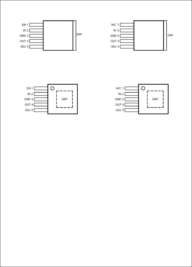
Connection Diagrams for TO-263 (TS) Package
30028122 |
30028121 |
Top View (LP38501TS-ADJ) |
Top View (LP38503TS-ADJ) |
TO-263 Package |
TO-263 Package |
Connection Diagrams for TO-263 THIN (TJ) Package
30028162 |
30028163 |
Top View (LP38501TJ-ADJ, LP38501ATJ-ADJ) |
Top View (LP38503TJ-ADJ, LP38503ATJ-ADJ) |
TO-263 THIN Package |
TO-263 THIN Package |
www.national.com |
2 |

Pin Descriptions for TO-263 (TS) and TO-263 THIN (TJ) Packages
Pin # |
Designation |
Function |
|
|
EN |
Enable (LP38501 only). Pull high to enable the output, low to disable the output. This pin has |
|
|
no internal bias and must be either tied to the input voltage, or actively driven. |
||
1 |
|
||
N/C |
In the LP38503, this pin has no internal connections. It can be left floating or used for trace |
||
|
|||
|
routing. |
||
|
|
||
|
|
|
|
2 |
IN |
Input Supply Pin |
|
|
|
|
|
3 |
GND |
Ground |
|
4 |
OUT |
Regulated Output Voltage Pin |
|
|
|
|
|
5 |
ADJ |
Sets output voltage |
|
|
|
|
|
|
|
The DAP is used as a thermal connection to remove heat from the device to the circuit board |
|
DAP |
DAP |
copper clad area which acts as the heatsink. The DAP is electrically connected to the |
|
backside of the die. The DAP must be connected to ground potential, but can not be used as |
|||
|
|
||
|
|
the only ground connection. |
|
Ordering Information |
|
||
TABLE 1. Package Marking and Ordering Information
Output |
Order Number |
Package Type |
Package Marking |
Supplied As: |
|
Voltage |
|
||||
|
|
|
|
||
|
LP38501TSX-ADJ |
|
LP38501TS-ADJ |
Tape and Reel of 500 Units |
|
|
|
|
|
|
|
ADJ |
LP38501TS-ADJ |
TO-263 |
LP38501TS-ADJ |
Rail of 45 Units |
|
|
|
|
|||
LP38503TSX-ADJ |
LP38503TS-ADJ |
Tape and Reel of 500 Units |
|||
|
|
||||
|
LP38503TS-ADJ |
|
LP38503TS-ADJ |
Rail of 45 Units |
|
|
|
|
|
|
|
|
LP38501TJ-ADJ |
|
LP38501TJ-ADJ |
Tape and Reel of 1000 Units |
|
|
|
|
|
|
|
ADJ |
LP38503TJ-ADJ |
TO-263 THIN |
LP38503TJ-ADJ |
Tape and Reel of 1000 Units |
|
LP38501ATJ-ADJ |
LP38501ATJ-AD |
Tape and Reel of 1000 Units |
|||
|
|
||||
|
|
|
|
|
|
|
LP38503ATJ-ADJ |
|
LP38503ATJ-AD |
Tape and Reel of 1000 Units |
ADJ-LP38501/3
3 |
www.national.com |

LP38501/3-ADJ
Absolute Maximum Ratings (Note 1)
If Military/Aerospace specified devices are required, please contact the National Semiconductor Sales Office/ Distributors for availability and specifications.
Storage Temperature Range |
−65°C to +150°C |
Lead Temperature |
|
(Soldering, 5 sec.) |
260°C |
ESD Rating (Note 2) |
±2 kV |
Power Dissipation(Note 3) |
Internally Limited |
Input Pin Voltage (Survival) |
−0.3V to +6.0V |
Enable Pin Voltage (Survival) |
−0.3V to +6.0V |
Output Pin Voltage (Survival) |
−0.3V to +6.0V |
IOUT(Survival) |
Internally Limited |
Operating Ratings (Note 1)
Input Supply Voltage |
2.7V to 5.5V |
Enable Input Voltage |
0.0V to 5.5V |
Output Current (DC) |
0 to 3A |
Junction Temperature(Note 3) |
−40°C to +125°C |
VOUT |
0.6V to 5V |
Electrical Characteristics
LP38501/3–ADJ
Unless otherwise specified: VIN = 3.3V, IOUT = 10 mA, CIN = 10 µF, COUT = 10 µF, VEN = VIN, VOUT = 1.8V. Limits in standard type are for TJ = 25°C only; limits in boldface type apply over the junction temperature (TJ) range of -40°C to +125°C. Minimum and
Maximum limits are guaranteed through test, design, or statistical correlation. Typical values represent the most likely parametric norm at TJ = 25°C, and are provided for reference purposes only.
Symbol |
Parameter |
Conditions |
Min |
Typ |
Max |
Units |
|
VADJ |
Adjust Pin Voltage (Note 6) |
2.7V ≤ VIN ≤ 5.5V |
0.584 |
0.605 |
0.626 |
V |
|
10 mA ≤ IOUT ≤ 3A |
0.575 |
0.635 |
|||||
|
|
|
|
||||
VADJ |
Adjust Pin Voltage (Note 6) |
2.7V ≤ VIN ≤ 5.5V |
0.596 |
0.605 |
0.614 |
V |
|
"A" GRADE |
10 mA ≤ IOUT ≤ 3A |
0.587 |
0.623 |
||||
IADJ |
Adjust Pin Bias Current |
2.7V ≤ VIN ≤ 5.5V |
|
50 |
750 |
nA |
|
VDO |
Dropout Voltage (Note 7) |
IOUT = 3A |
|
420 |
550 |
mV |
|
|
665 |
||||||
|
|
|
|
|
|
||
|
Output Voltage Line |
2.7V ≤ VIN ≤ 5.5V |
|
0.04 |
|
|
|
VOUT/ΔVIN |
Regulation |
— |
— |
%/V |
|||
0.05 |
|||||||
|
(Note 4, Note 6) |
|
|
|
|
||
|
|
|
|
|
|
||
|
|
|
|
|
|
|
|
|
Output Voltage Load |
10 mA ≤ IOUT ≤ 3A |
|
0.12 |
|
|
|
VOUT/ΔIOUT |
Regulation |
— |
— |
%/A |
|||
0.24 |
|||||||
|
(Note 5, Note 6) |
|
|
|
|
||
|
|
|
|
|
|
||
|
|
|
|
|
|
|
|
IGND |
Ground Pin Current In Normal |
10 mA ≤ IOUT ≤ 3A |
— |
2 |
4 |
mA |
|
Operation Mode |
5 |
||||||
|
|
|
|
|
|||
|
|
|
|
|
|
|
|
IDISABLED |
Ground Pin Current |
VEN < VIL(EN) |
— |
0.025 |
0.125 |
µA |
|
15 |
|||||||
|
|
|
|
|
|
||
|
|
|
|
|
|
|
|
IOUT(PK) |
Peak Output Current |
VOUT ≥ VOUT(NOM) - 5% |
|
6 |
|
A |
|
ISC |
Short Circuit Current |
VOUT = 0V |
3.5 |
6 |
|
A |
|
Enable Input (LP38501 Only) |
|
|
|
|
|
||
|
|
|
|
|
|
|
|
VIH(EN) |
Enable Logic High |
VOUT = ON |
1.4 |
— |
— |
V |
|
VIL(EN) |
Enable Logic Low |
VOUT = OFF |
— |
— |
0.65 |
||
|
|||||||
|
|
Time from VEN < VIL(EN) to VOUT = |
— |
|
— |
|
|
td(off) |
Turn-off delay |
OFF |
25 |
|
|||
|
|
ILOAD = 3A |
|
|
|
µs |
|
|
|
Time from VEN >VIH(EN) to VOUT = |
— |
|
— |
||
|
|
|
|
||||
td(on) |
Turn-on delay |
ON |
25 |
|
|||
|
|
ILOAD = 3A |
|
|
|
|
|
IIH(EN) |
Enable Pin High Current |
VEN = VIN |
— |
35 |
— |
nA |
|
IIL(EN) |
Enable Pin Low Current |
VEN = 0V |
— |
35 |
— |
||
|
|||||||
www.national.com |
4 |

|
|
|
|
|
|
|
|
|
|
|
LP38501/3 |
|
Symbol |
Parameter |
Conditions |
— |
58 |
— |
Units |
||||
|
Min |
Typ |
Max |
|
|
||||||
|
AC Parameters |
|
|
|
|
|
|
|
|
|
|
|
|
|
VIN = 3.0V, IOUT = 3A |
|
|
|
|
|
|
|
|
|
|
|
f = 120Hz |
|
|
|
|
|
|
- |
|
|
PSRR |
Ripple Rejection |
|
— |
56 |
— |
dB |
|
ADJ |
||
|
VIN = 3.0V, IOUT = 3A |
|
|
|
|
|
|||||
|
|
|
|
|
|
|
|
|
|
|
|
|
|
|
f = 1 kHz |
|
|
|
|
|
|
|
|
|
|
|
|
|
|
|
|
|
|
|
|
|
ρn(l/f) |
Output Noise Density |
f = 120Hz, COUT = 10 µF CER |
— |
1.0 |
— |
µV/√ |
|
|
|
|
|
Hz |
|
|
||||||||
|
en |
Output Noise Voltage |
BW = 100Hz – 100kHz |
— |
100 |
— |
µV (rms) |
|
|
||
|
COUT = 10 µF CER |
|
|
||||||||
|
|
|
|
|
|
|
|
|
|
|
|
|
Thermal Characteristics |
|
|
|
|
|
|
|
|
|
|
|
TSD |
Thermal Shutdown |
TJ rising |
— |
170 |
— |
°C |
|
|
||
|
TSD |
Thermal Shutdown Hysteresis |
TJ falling from TSD |
— |
10 |
— |
|
|
|||
|
|
|
|
|
|
||||||
|
θJ-A |
Thermal Resistance |
TO-263, TO-263 THIN(Note 8) |
|
37 |
|
|
|
|
|
|
|
Junction to Ambient |
1 sq. in. copper |
|
|
|
|
|
|
|
||
|
|
|
|
|
°C/W |
|
|
||||
|
|
|
|
|
|
|
|
|
|||
|
θJ-C |
Thermal Resistance |
TO-263, TO-263 THIN |
— |
5 |
— |
|
|
|||
|
|
|
|
|
|
||||||
|
Junction to Case |
|
|
|
|
|
|||||
|
|
|
|
|
|
|
|
|
|
|
|
|
|
|
|
|
|
|
|
|
|
|
|
Note 1: Absolute Maximum Ratings indicate limits beyond which damage to the device may occur. Operating Ratings indicate conditions for which the device is intended to be functional, but does not guarantee specific performance limits. For guaranteed specifications and conditions, see the Electrical Characteristics.
Note 2: The human body model is a 100pF capacitor discharged through a 1.5kΩ resistor into each pin.
Note 3: Operating junction temperature must be evaluated, and derated as needed, based on ambient temperature (TA), power dissipation (PD), maximum allowable operating junction temperature (TJ(MAX)), and package thermal resistance (θJA). See Application Information.
Note 4: Output voltage line regulation is defined as the change in output voltage from the nominal value due to change in the voltage at the input.
Note 5: Output voltage load regulation is defined as the change in output voltage from the nominal value due to change in the load current at the output.
Note 6: The line and load regulation specification contains only the typical number. However, the limits for line and load regulation are included in the output voltage tolerance specification.
Note 7: Dropout voltage is defined as the minimum input to output differential voltage at which the output drops 2% below the nominal value. For any output voltage less than 2.5V, the minimum VIN operating voltage is the limiting factor.
Note 8: The value of θJA for the TO-263 (TS) package and TO-263 THIN (TJ) package can range from approximately 30 to 60°C/W depending on the amount of PCB copper dedicated to heat transfer (See Application Information).
5 |
www.national.com |
LP38501/3-ADJ
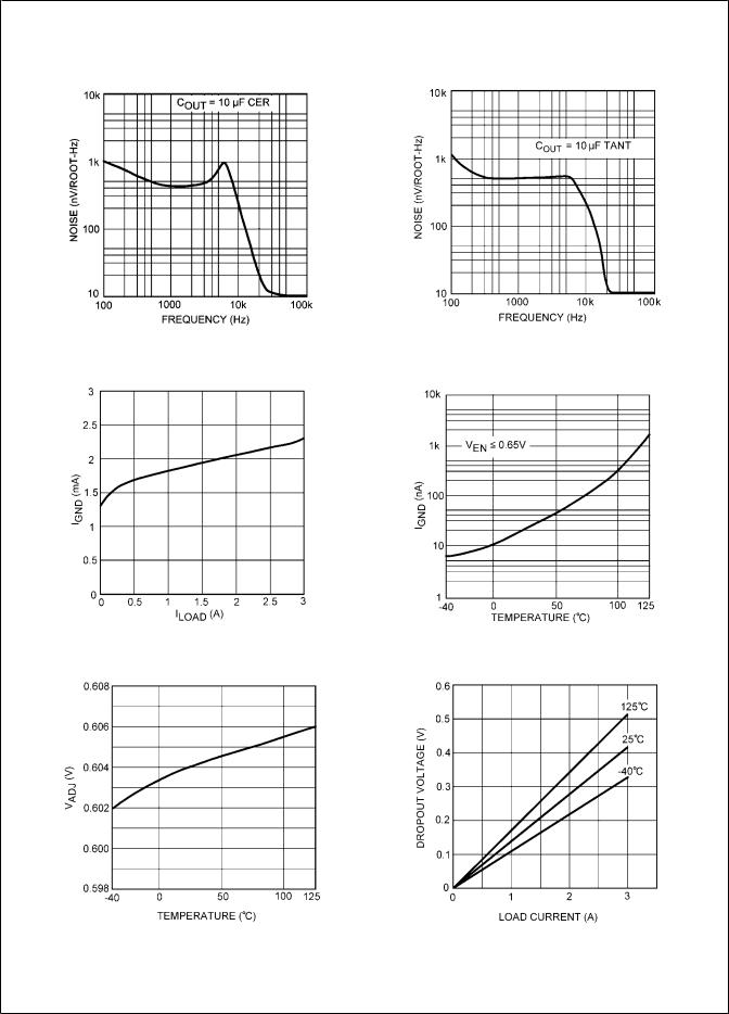
Typical Performance Characteristics |
Unless otherwise specified: TJ = 25°C, VIN = 2.7V, VEN = VIN, |
CIN = 10 µF, COUT = 10 µF, IOUT = 10 mA, VOUT = 1.8V |
|
Noise Density |
Noise Density |
|
30028110 |
30028114 |
|
|
|
IGND vs Load Current |
|
IGND(OFF) vs Temperature |
30028111 30028112
VADJ vs Temperature Dropout Voltage vs Load Current
30028113 |
30028115 |
www.national.com |
6 |
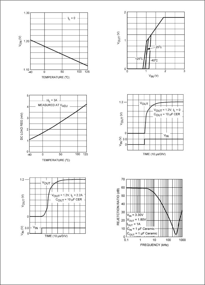
VEN vs Temperature |
Turn-on Characteristics |
|
30028117 |
|
30028116 |
Load Regulation vs Temperature |
Turn-on Time |
30028155
|
30028118 |
Turn-on Time |
PSRR |
30028156
30028120
ADJ-LP38501/3
7 |
www.national.com |
LP38501/3-ADJ
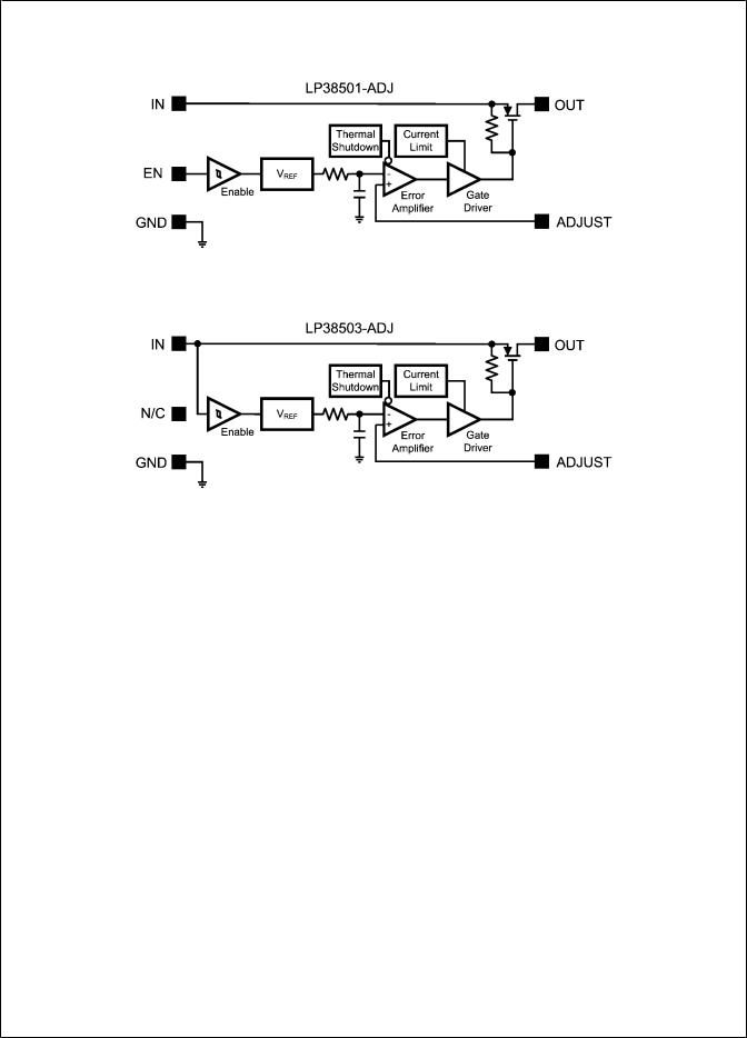
Block Diagrams
LP38501-ADJ Block Diagram
30028150
LP38503-ADJ Block Diagram
30028151
www.national.com |
8 |
Application Information
EXTERNAL CAPACITORS
The LP3850X requires that at least 10 µF (±20%) capacitors be used at the input and output pins located within one cm of the IC. Larger capacitors may be used without limit on size for both CIN and COUT. Capacitor tolerances such as temperature variation and voltage loading effects must be considered when selecting capacitors to ensure that they will provide the minimum required amount of capacitance under all operating conditions for the application.
In general, ceramic capacitors are best for noise bypassing and transient response because of their ultra low ESR. It must be noted that if ceramics are used, only the types with X5R or X7R dielectric ratings should be used (never Z5U or Y5F). Capacitors which have the Z5U or Y5F characteristics will see a drop in capacitance of as much as 50% if their temperature increases from 25°C to 85°C. In addition, the capacitance drops significantly with applied voltage: a typical Z5U or Y5F capacitor can lose as much as 60% of it’s rated capacitance if only half of the rated voltage is applied to it. For these reasons, only X5R and X7R ceramics should be used.
INPUT CAPACITOR
All linear regulators can be affected by the source impedance of the voltage which is connected to the input. If the source impedance is too high, the reactive component of the source may affect the control loop’s phase margin. To ensure proper loop operation, the ESR of the capacitor used for CIN must not exceed 0.5 Ohms. Any good quality ceramic capacitor will meet this requirement, as well as many good quality tantalums. Aluminum electrolytic capacitors may also work, but can possibly have an ESR which increases significantly at cold temperatures. If the ESR of the input capacitor may exceed 0.5 Ohms, it is recommended that a 2.2 µF ceramic capacitor be used in parallel, as this will assure stable loop operation.
OUTPUT CAPACITOR
Any type of capacitor may be used for COUT, with no limitations on minimum or maximum ESR, as long as the minimum
amount of capacitance is present. The amount of capacitance can be increased without limit. Increasing the size of COUT typically will give improved load transient response.
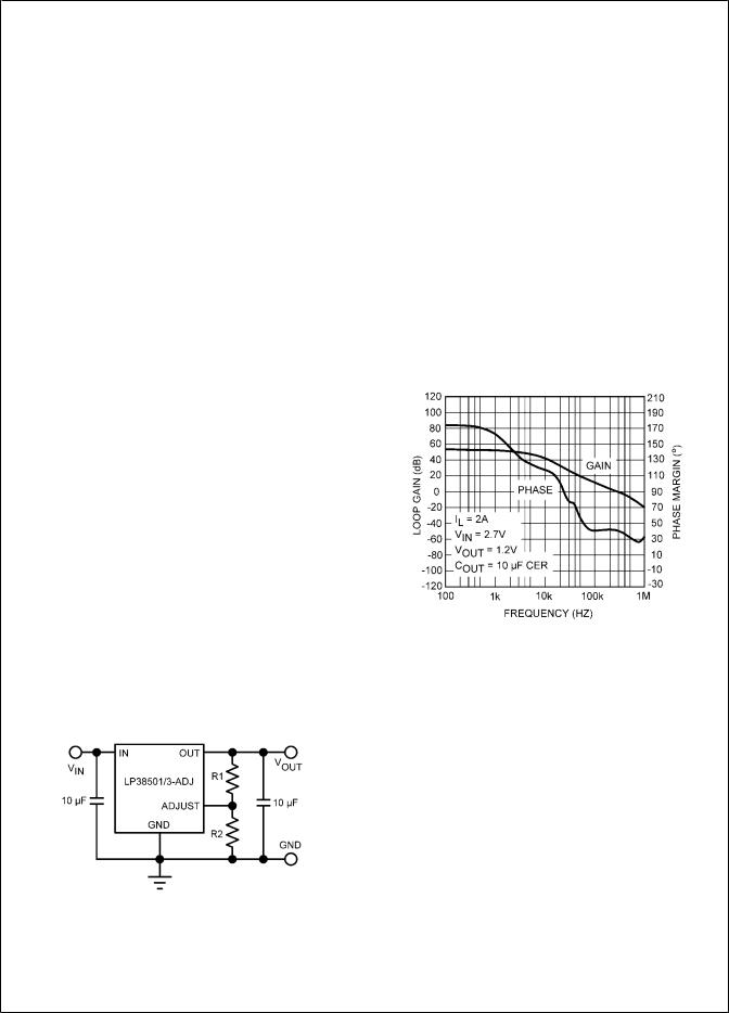
SETTING THE OUTPUT VOLTAGE
The output voltage of the LP38501/3-ADJ can be set to any value between 0.6V and 5V using two external resistors shown as R1 and R2 in Figure 1.
30028157
FIGURE 1.
The value of R2 should always be less than or equal to 10 kΩ for good loop compensation. R1 can be selected for a given VOUT using the following formula:
VOUT = VADJ (1 + R1/R2) + IADJ (R1)
Where VADJ is the adjust pin voltage and IADJ is the bias current flowing into the adjust pin.
STABILITY AND PHASE MARGIN
Any regulator which operates using a feedback loop must be compensated in such a way as to ensure adequate phase margin, which is defined as the difference between the phase shift and -180 degrees at the frequency where the loop gain crosses unity (0 dB). For most LDO regulators, the ESR of the output capacitor is required to create a zero to add enough phase lead to ensure stable operation. The LP38501 has a unique internal compensation circuit which maintains phase margin regardless of the ESR of the output capacitor, so any type of capacitor may be used.
Figure 2 shows the gain/phase plot of the LP38501-ADJ with an output of 1.2V, 10 µF ceramic output capacitor, delivering 2A of load current. It can be seen that the unity-gain crossover occurs at 300 kHz, and the phase margin is about 40° (which is very stable).
30028153
FIGURE 2. Gain-Bandwidth Plot for 2A Load
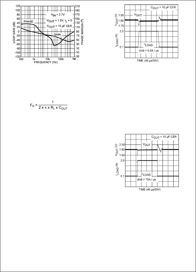
Figure 3 shows the gain and phase with no external load. In this case, the only load is provided by the gain setting resistors (about 12 kΩ total in this test). It is immediately obvious that the unity-gain frequency is significantly lower (dropping to about 500 Hz), at which point the phase margin is 125°.
ADJ-LP38501/3
9 |
www.national.com |
LP38501/3-ADJ
30028154
FIGURE 3. Gain-Bandwidth Plot for No Load
The reduction in unity-gain bandwidth as load current is reduced is normal for any LDO regulator using a P-FET or PNP pass transistor, because they have a pole in the loop gain function given by:
This illustrates how the pole goes to the highest frequency when RL is minimum value (maximum load current). In general, LDO’s have maximum bandwidth (and lowest phase margin) at full load current. In the case of the LP38501, it can be seen that it has good phase margin even when using ceramic capacitors with ESR values of only a few milli Ohms.
LOAD TRANSIENT RESPONSE
Load transient response is defined as the change in regulated output voltage which occurs as a result of a change in load current. Many applications have loads which vary, and the control loop of the voltage regulator must adjust the current in the pass FET transistor in response to load current changes. For this reason, regulators with wider bandwidths often have better transient response.
The LP38501 employs an internal feedforward design which makes the load transient response much faster than would be predicted simply by loop speed: this feedforward means any voltage changes appearing on the output are coupled through to the high-speed driver used to control the gate of the pass FET along a signal path using very fast FET devices. Because of this, the pass transistor’s current can change very quickly.
Figure 4 shows the output transient response resulting from a change in load current of 0.1A – 3A, and then 3A – 0.1A with a load current slew rate of 500 mA/µs. As shown in the plots, the resulting change in output voltage is only about 40 mV (peak), which is just slightly over 2% for the 1.8V output used for this test. This is excellent performance for such a small output capacitor.
30028136
FIGURE 4. Load Transient Response: 10 µF Ceramic,
0.5A/µs di/dt
When the load current changes much more quickly, the output voltage will show more change because the loop and internal feedforward circuitry are not able to react as fast as the load changes. In such cases, it is the output capacitor which must supply load current during the transition until the loop responds and changes the pass transistor’s drive to deliver the new value of load current. As an example, the slew rate of the load current will be increased to 75A/µs and the same test will be performed. In Figure 5, it can be seen that the peak excursion of the output voltage during the transient has now increased to about 200 mV, which is just slightly over 11% for the 1.8V output.
30028134
FIGURE 5. Load Transient Response: 10 µF Ceramic,
75A/µs di/dt
A better understanding of the load transient can be obtained when the load’s rising edge is expanded in time scale (Figure 6).
www.national.com |
10 |