

Розрахункова СЗіВІ / Розрахункова робота / Стабілізатори напруги / LDO National Semiconductor / LP5900
.pdfAugust 7, 2009
LP5900
Ultra Low Noise, 150 mA Linear Regulator for RF/Analog Circuits Requires No Bypass Capacitor
General Description
The LP5900 is a linear regulator capable of supplying 150 mA output current. Designed to meet the requirements of RF/ Analog circuits, the LP5900 device provides low noise, high PSRR, low quiescent current, and low line transient response figures. Using new innovative design techniques the LP5900 offers class-leading device noise performance without a noise bypass capacitor.
The device is designed to work with 0.47 μF input and output ceramic capacitors. (No Bypass Capacitor is required)
The device is available in micro SMD package and LLP package. Also available in Exteme Thin micro SMD package. For all other package options contact your local NSC sales office.
This device is available with 1.5V,1.575V, 1.8V, 1.9V, 2.0V, 2.1V, 2.2V, 2.3V, 2.5V, 2.6V, 2.7V, 2.75V 2.8V, 2.85V 3.0V, 3.3V and 4.5V outputs. Please contact your local sales office for any other voltage options.
Features
■Stable with 0.47 μF Ceramic Input and Output Capacitors
■No Noise Bypass Capacitor Required
■Logic Controlled Enable
■Thermal-overload and short-circuit protection
■−40°C to +125°C junction temperature range for operation
Key Specifications
■ Input voltage range |
2.5V to 5.5V |
■ Output voltage range |
1.5V to 4.5V |
■ Output current |
150 mA |
■ Low output voltage noise |
6.5 μVRMS |
■ PSRR |
75 dB at 1 kHz |
■ Output voltage tolerance |
± 2% |
■ Virtually zero IQ (disabled) |
<1 μA |
■ Very low IQ (enabled) |
25 μA |
■ Start-up time |
150 μs |
■ Low dropout |
80 mV typ. |
Package
4-Bump micro SMD |
1.057 mm x 1.083 mm x |
(lead free) |
0.600mm |
Extreme 4-Bump micro SMD |
1.067 mm x 1.092 mm x |
(lead free) |
0.250mm |
6 Pin LLP (SC-70 footprint) |
2.2 mm x 2.5 mm x |
Applications
■Cellular phones
■PDA handsets
■Wireless LAN devices
Typical Application Circuit
20144101
Bypass No Requires Circuits RF/Analog for Regulator Linear mA 150 Noise, Low Ultra LP5900
Capacitor
© 2009 National Semiconductor Corporation |
201441 |
www.national.com |
LP5900
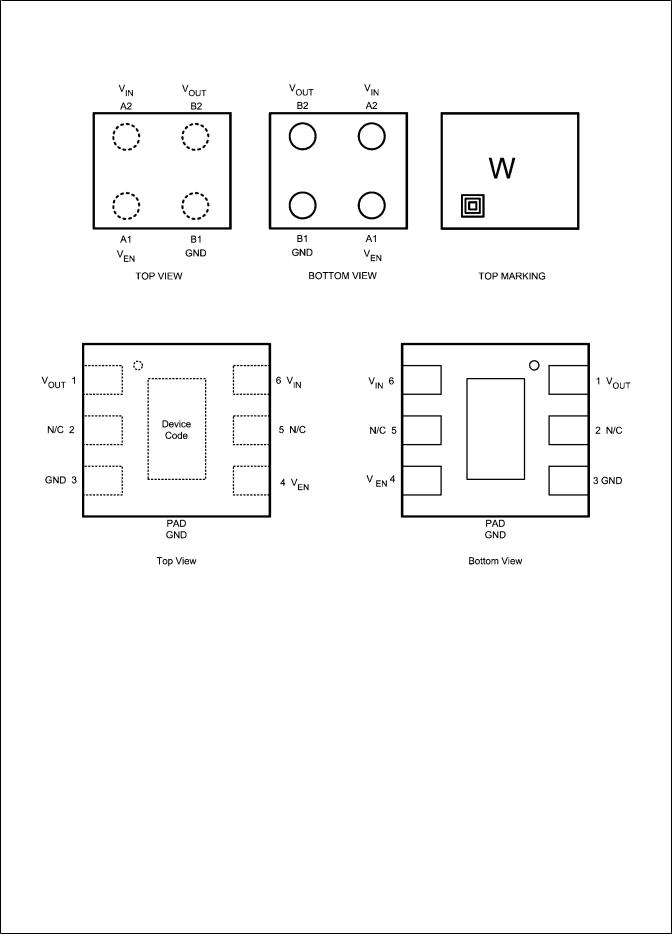
Connection Diagrams
4-Bump Thin micro SMD Package and Extreme Thin micro SMD Package, Large Bump NS Package Number TLA04/XRA04
20144102
The actual physical placement of the package marking will vary from part to part.
LLP-6 Package
NS Package Number SDB06A
20144106
Pin Descriptions
Pin No. |
|
Symbol |
Name and Function |
|
micro SMD |
|
LLP |
||
|
|
|
||
A1 |
|
4 |
VEN |
Enable input; disables the regulator when ≤ 0.4V. Enables the |
|
|
|
|
regulator when ≥ 1.2V. An internal 1 MΩ pulldown resistor connects |
|
|
|
|
this input to ground. |
|
|
|
|
|
B1 |
|
3 |
GND |
Common ground |
B2 |
|
1 |
VOUT |
Output voltage. A 0.47 μF Low ESR capacitor should be connected to |
|
|
|
|
this Pin. Connect this output to the load circuit. |
|
|
|
|
|
A2 |
|
6 |
VIN |
Input voltage supply. A 0.47 µF capacitor should be connected at this |
|
|
|
|
input. |
|
|
Pad |
GND |
Common Ground. Connect to Pin 3. |
|
|
|
|
|
www.national.com |
2 |

Ordering Information
micro SMD Package (Lead Free)
Output Voltage |
Supplied As |
Package Marking |
||
(V) |
||||
|
|
|
||
|
250 Units Tape and Reel |
3k Units Tape and Reel |
|
|
1.5 |
LP5900TL-1.5/NOPB |
LP5900TLX-1.5/NOPB |
|
|
1.575 |
LP5900TL-1.575/NOPB |
LP5900TLX-1.575/NOPB |
|
|
|
|
|
|
|
1.8 |
LP5900TL-1.8/NOPB |
LP5900TLX-1.8/NOPB |
|
|
|
|
|
|
|
1.9 |
LP5900TL-1.9/NOPB |
LP5900TLX-1.9/NOPB |
|
|
2.0 |
LP5900TL-2.0/NOPB |
LP5900TLX-2.0/NOPB |
|
|
|
|
|
|
|
2.1 |
LP5900TL-2.1/NOPB |
LP5900TLX-2.1/NOPB |
|
|
2.2 |
LP5900TL-2.2/NOPB |
LP5900TLX-2.2/NOPB |
|
|
|
|
|
|
|
2.3 |
LP5900TL-2.3/NOPB |
LP5900TLX-2.3/NOPB |
|
|
|
|
|
|
|
2.5 |
LP5900TL-2.5/NOPB |
LP5900TLX-2.5/NOPB |
|
|
2.6 |
LP5900TL-2.6/NOPB |
LP5900TLX-2.6/NOPB |
|
|
|
|
|
|
|
2.7 |
LP5900TL-2.7/NOPB |
LP5900TLX-2.7/NOPB |
|
|
|
|
|
|
|
2.75 |
LP5900TL-2.75/NOPB |
LP5900TLX-2.75/NOPB |
|
|
2.8 |
LP5900TL-2.8/NOPB |
LP5900TLX-2.8/NOPB |
|
|
|
|
|
|
|
2.85 |
LP5900TL-2.85/NOPB |
LP5900TLX-2.85/NOPB |
|
|
|
|
|
|
|
3.0 |
LP5900TL-3.0/NOPB |
LP5900TLX-3.0/NOPB |
|
|
3.3 |
LP5900TL-3.3/NOPB |
LP5900TLX-3.3/NOPB |
|
|
|
|
|
|
|
4.5 |
LP5900TL-4.5/NOPB |
LP5900TLX-4.5/NOPB |
|
|
Extreme Thin Micro SMD (Lead Free)
Output Voltage |
Supplied As |
Package Marking |
||
(V) |
||||
|
|
|
||
|
250 Units Tape and Reel |
3k Units Tape and Reel |
|
|
1.8 |
LP5900XR-1.8/NOPB |
LP5900XRX-1.8/NOPB |
|
|
For LLP-6 Package (Lead Free)
Output Voltage |
Supplied As |
Package Marking |
||
(V) |
||||
|
|
|
||
|
250 Units Tape and Reel |
3k Units Tape and Reel |
|
|
1.5 |
LP5900SD-1.5/NOPB |
LP5900SDX-1.5/NOPB |
L15 |
|
1.8 |
LP5900SD-1.8/NOPB |
LP5900SDX-1.8/NOPB |
L17 |
|
|
|
|
|
|
2.0 |
LP5900SD-2.0/NOPB |
LP5900SDX-2.0/NOPB |
L18 |
|
|
|
|
|
|
2.2 |
LP5900SD-2.2/NOPB |
LP5900SDX-2.2/NOPB |
L19 |
|
2.5 |
LP5900SD-2.5/NOPB |
LP5900SDX-2.5/NOPB |
L13 |
|
|
|
|
|
|
2.7 |
LP5900SD-2.7/NOPB |
LP5900SDX-2.7/NOPB |
L14 |
|
|
|
|
|
|
2.8 |
LP5900SD-2.8/NOPB |
LP5900SDX-2.8/NOPB |
L12 |
|
3.0 |
LP5900SD-3.0/NOPB |
LP5900SDX-3.0/NOPB |
L20 |
|
|
|
|
|
|
3.3 |
LP5900SD-3.3/NOPB |
LP5900SDX-3.3/NOPB |
L16 |
|
|
|
|
|
|
LP5900
3 |
www.national.com |

LP5900
Absolute Maximum Ratings (Notes 1, 2)
If Military/Aerospace specified devices are required, please contact the National Semiconductor Sales Office/ Distributors for availability and specifications.
VIN Pin: Input Voltage |
-0.3 to 6.0V |
VOUT Pin: Output Voltage |
-0.3 to (VIN + 0.3V) to 6.0V |
|
(max) |
VEN Pin: Enable Input Voltage |
-0.3 to (VIN + 0.3V) to 6.0V |
|
(max) |
Continuous Power Dissipation |
|
(Note 3) |
Internally Limited |
Junction Temperature (TJMAX) |
150°C |
Storage Temperature Range |
-65 to 150°C |
Maximum Lead Temperature |
|
(Soldering, 10 sec.) |
260°C |
ESD Rating (Note 4) |
|
Human Body Model |
2 kV |
Machine Model |
200V |
Operating Ratings (Note 1), |
(Note 2) |
VIN: Input Voltage Range |
2.5V to 5.5V |
VEN: Enable Voltage Range |
0 to (VIN + 0.3V) to |
|
5.5V (max) |
Recommended Load Current |
0 to 150 mA |
(Note 5) |
|
Junction Temperature Range (TJ) |
-40°C to +125°C |
Ambient Temperature Range (TA) |
-40°C to +85°C |
(Note 5) |
|
Thermal Properties
Junction to Ambient Thermal Resistance θJA (Note 6)
JEDEC Board (microSMD) |
|
(Note 16) |
88°C/W |
4L Cellphone Board (microSMD) |
157.4°C/W |
JEDEC Board (LLP-6)(Note 16) |
77.3°C/W |
Electrical Characteristics
Limits in standard typeface are for TA = 25ºC. Limits in boldface type apply over the full operating junction temperature range
(-40ºC ≤ TJ ≤ +125ºC). Unless otherwise noted, specifications apply to the LP5900 Typical Application Circuit (pg. 1) with: VIN = VOUT (NOM) + 1.0V, VEN = 1.2V, CIN = COUT = 0.47 μF, IOUT = 1.0 mA. (Note 2), (Note 7)
Symbol |
Parameter |
Conditions |
Min |
Typ |
Max |
Units |
||
VIN |
Input Voltage |
|
|
|
2.5 |
|
5.5 |
V |
VOUT |
Output Voltage Tolerance |
VIN = (VOUT(NOM) + 1.0V) to 5.5V, IOUT = 1 |
−2 |
|
2 |
% |
||
|
|
mA to 150mA |
|
|
|
|
||
|
|
|
|
|
|
|
||
|
Line Regulation |
VIN = (VOUT(NOM) + 1.0V) to 5.5V, IOUT = 1 |
|
0.05 |
|
%/V |
||
|
|
mA |
|
|
|
|||
|
|
|
|
|
|
|
||
|
Load Regulation |
IOUT = 1 mA to 150 mA |
|
|
0.001 |
|
%/mA |
|
ILOAD |
Load Current |
(Note 9) |
|
0 |
|
|
mA |
|
|
Maximum Output Current |
|
|
|
150 |
|
|
|
|
|
|
|
|
|
|
||
IQ |
Quiescent Current (Note 11) |
VEN = 1.2V, IOUT = 0 mA |
|
|
25 |
50 |
|
|
|
|
VEN = 1.2V, IOUT = 150 mA |
|
160 |
230 |
µA |
||
|
|
VEN = 0.3V (Disabled) |
|
|
0.003 |
1.0 |
|
|
IG |
Ground Current (Note 13) |
IOUT = 0 mA (VOUT = 2.5V) |
|
30 |
|
µA |
||
VDO |
Dropout Voltage(Note 10) |
IOUT = 150 mA |
|
|
80 |
150 |
mV |
|
ISC |
Short Circuit Current Limit |
(Note 12) |
|
|
300 |
|
mA |
|
PSRR |
Power Supply Rejection Ratio |
f = 100 Hz, IOUT = 150 mA |
|
85 |
|
|
||
|
(Note 15) |
f = 1 kHz, IOUT = 150 mA |
|
75 |
|
|
||
|
|
|
|
|
||||
|
|
f = 10 kHz, IOUT = 150 mA |
|
65 |
|
dB |
||
|
|
f = 50 kHz, IOUT = 150 mA |
|
52 |
|
|
||
|
|
f = 100 kHz, IOUT = 150 mA |
|
40 |
|
|
||
en |
Output Noise Voltage |
BW = 10 Hz to 100 kHz, |
IOUT = 0 mA |
|
7 |
|
μVRMS |
|
|
(Note 15) |
VIN = 4.2V |
|
IOUT = 1 mA |
|
10 |
|
|
|
|
|
|
IOUT = 150 mA |
|
6.5 |
|
|
TSHUTDOWN |
Thermal Shutdown |
Temperature |
|
|
160 |
|
ºC |
|
|
|
Hysteresis |
|
|
20 |
|
||
|
|
|
|
|
|
|||
www.national.com |
4 |

|
|
|
|
|
|
|
|
|
|
LP5900 |
|
Symbol |
Parameter |
Conditions |
|
Min |
Typ |
Max |
Units |
||
|
|
|
|
|||||||
|
Login Input Thresholds |
|
|
|
|
|
|
|
|
|
|
|
|
|
|
|
|
|
|
|
|
|
VIL |
Low Input Threshold (VEN) |
VIN = 2.5V to 5.5V |
|
|
|
0.4 |
V |
|
|
|
VIH |
High Input Threshold (VEN) |
VIN = 2.5V to 5.5V |
|
1.2 |
|
|
V |
|
|
|
IEN |
Input Current at VEN Pin |
VEN = 5.5V and VIN = 5.5V |
|
|
5.5 |
|
μA |
|
|
|
|
(Note 14) |
VEN = 0.0V and VIN = 5.5V |
|
|
0.001 |
|
|
|
|
|
|
|
|
|
|
|
|
|||
|
Transient Characteristics |
|
|
|
|
|
|
|
|
|
|
|
|
|
|
|
|
|
|
||
|
VOUT |
Line Transient |
VIN = (VOUT(NOM) + 1.0V) to (VOUT(NOM) + |
−2 |
|
|
|
|
|
|
|
|
(Note 15) |
1.6V) in 30 μs, IOUT = 1 mA |
|
|
|
|
|
|
|
|
|
|
|
|
|
mV |
|
|
||
|
|
|
VIN = (VOUT(NOM) + 1.6V) to (VOUT(NOM) |
+ |
|
|
2 |
|
|
|
|
|
|
|
|
|
|
|
|||
|
|
|
1.0V) in 30 μs, IOUT = 1 mA |
|
|
|
|
|
|
|
|
|
|
|
|
|
|
|
|
|
|
|
|
Load Transient |
IOUT = 1 mA to 150 mA in 10 μs |
|
−110 |
|
|
mV |
|
|
|
|
(Note 15) |
IOUT = 150 mA to 1 mA in 10 μs |
|
|
|
50 |
|
|
|
|
|
|
|
|
|
|
|
|||
|
|
|
|
|
|
|
|
|
||
|
|
Overshoot on Startup |
|
|
|
|
20 |
mV |
|
|
|
|
(Note 15) |
|
|
|
|
|
|
||
|
|
|
|
|
|
|
|
|
|
|
|
|
|
|
|
|
|
|
|
|
|
|
|
Turn on Time |
To 95% of VOUT(NOM) |
|
|
150 |
300 |
μs |
|
|
Note 1: Absolute Maximum Ratings indicate limits beyond which damage to the component may occur. Operating Ratings are conditions under which operation of the device is guaranteed. Operating Ratings do not imply guaranteed performance limits. For guaranteed performance limits and associated test conditions, see the Electrical Characteristics tables.
Note 2: All voltages are with respect to the potential at the GND pin.
Note 3: Internal thermal shutdown circuitry protects the device from permanent damage.
Note 4: The Human body model is a 100 pF capacitor discharged through a 1.5 kΩ resistor into each pin. The machine model is a 200 pF capacitor discharged directly into each pin. MIL-STD-883 3015.7
Note 5: In applications where high power dissipation and/or poor package thermal resistance is present, the maximum ambient temperature may have to be derated. Maximum ambient temperature (TA-MAX) is dependent on the maximum operating junction temperature (TJ-MAX-OP = 125°C), the maximum power dissipation of the device in the application (PD-MAX), and the junction-to ambient thermal resistance of the part/package in the application (θJA), as given by the following equation: TA-MAX = TJ-MAX-OP – (θJA × PD-MAX). See applications section.
Note 6: Junction-to-ambient thermal resistance is highly application and board-layout dependent. In applications where high maximum power dissipation exists, special care must be paid to thermal dissipation issues in board design.
Note 7: Min and Max limits are guaranteed by design, test, or statistical analysis. Typical numbers are not guaranteed, but do represent the most likely norm.
Note 8: CIN, COUT: Low-ESR Surface-Mount Ceramic Capacitors (MLCCs) used in setting electrical characteristics.
Note 9: The device maintains a stable, regulated output voltage without a load current.
Note 10: Dropout voltage is the voltage difference between the input and the output at which the output voltage drops to 100 mV below its nominal value. This parameter only applies to output voltages above 2.5V.
Note 11: Quiescent current is defined here as the difference in current between the input voltage source and the load at VOUT.
Note 12: Short Circuit Current is measured with VOUT pulled to 0v and VIN worst case = 6.0V.
Note 13: Ground current is defined here as the total current flowing to ground as a result of all input voltages applied to the device.
Note 14: There is a 1 MΩ resistor between VEN and ground on the device.
Note 15: This specification is guaranteed by design.
Note 16: Detailed description of the board can be found in JESD51-7
Output & Input Capacitor, Recommended Specifications
Symbol |
Parameter |
Conditions |
Min |
Nom |
Max |
Units |
CIN |
Input Capacitance |
Capacitance for stability |
0.33 |
0.47 |
|
µF |
COUT |
Output Capacitance |
|
0.33 |
0.47 |
10 |
|
ESR |
Output/Input Capacitance |
|
5 |
|
500 |
mΩ |
Note: The minimum capacitance should be greater than 0.33 µF over the full range of operating conditions. The capacitor tolerance should be 30% or better over the full temperature range. The full range of operating conditions for the capacitor in the application should be considered during device selection to ensure this minimum capacitance specification is met. X7R capacitors are recommended however capacitor types X5R, Y5V and Z5U may be used with consideration of the application and conditions.
5 |
www.national.com |
LP5900
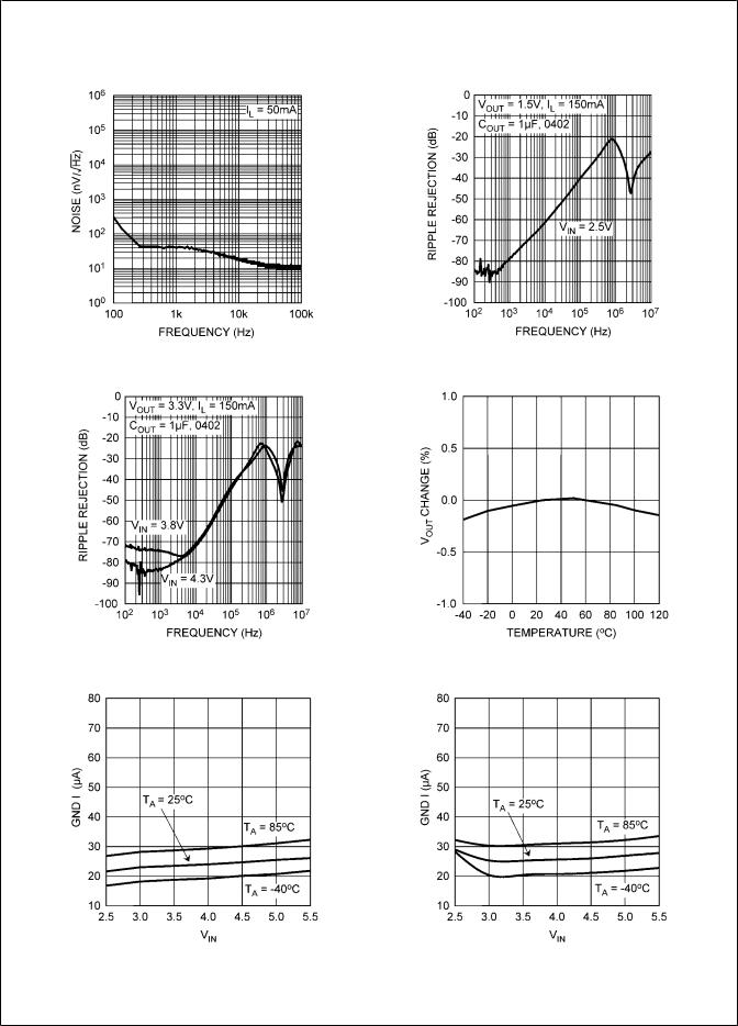
Typical Performance Characteristics. Unless otherwise specified,CIN = COUT = 0.47µF, VIN = VOUT (NOM) + 1.0V, VEN = 1.2V, IOUT = 1mA , T A = 25ºC.
Output Noise Density |
Power Supply Rejection Ratio |
|
20144157 |
20144158 |
Power Supply Rejection Ratio |
|
Output Voltage Change vs Temperature |
20144159 |
20144154 |
|
|
Ground Current vs VIN, I LOAD = 0mA |
Ground Current vs VIN, I LOAD = 1mA |
20144151 |
20144152 |
www.national.com |
6 |
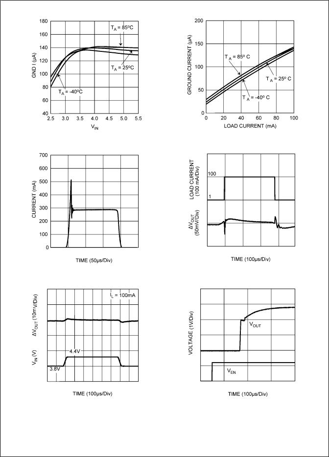
Ground Current vs VIN, I LOAD = 100mA |
Ground Current vs Load Current |
20144153 |
20144150 |
Short Circuit Current |
Load Transient |
|
20144148 |
20144149 |
|
|
|
Line Transient |
|
Enable Start-up Time, (I L= 1mA, VOUT = 2.8V) |
20144155 |
20144144 |
|
LP5900
7 |
www.national.com |
LP5900
Enable Start-up Time, (I L= 100mA, VOUT = 2.8V)
20144145
Enable Start-up Time, (I L= 100mA, VOUT = 2.8V)
20144147
Application Hints
POWER DISSIPATION AND DEVICE OPERATION
The permissible power dissipation for any package is a measure of the capability of the device to pass heat from the power source, the junctions of the IC, to the ultimate heat sink, the ambient environment. Thus the power dissipation is dependent on the ambient temperature and the thermal resistance across the various interfaces between the die and ambient air. As stated in (Note 5) of the electrical characteristics, the allowable power dissipation for the device in a given package can be calculated using the equation:
The actual power dissipation across the device can be represented by the following equation:
PD = (VIN – VOUT) x IOUT
This establishes the relationship between the power dissipation allowed due to thermal consideration, the voltage drop across the device, and the continuous current capability of the
Enable Start-up Time, (I L= 1mA, VOUT = 2.8V)
20144146
Dropout Over Temperature (100mA)
20144105
device. These two equations should be used to determine the optimum operating conditions for the device in the application.
EXTERNAL CAPACITORS
Like any low-dropout regulator, the LP5900 requires external capacitors for regulator stability. The LP5900 is specifically designed for portable applications requiring minimum board space and smallest components. These capacitors must be correctly selected for good performance.
INPUT CAPACITOR
An input capacitor is required for stability. The input capacitor should be at least equal to or greater than the output capacitor. It is recommended that a 0.47 µF capacitor be connected between the LP5900 input pin and ground.
This capacitor must be located a distance of not more than 1 cm from the input pin and returned to a clean analogue ground. Any good quality ceramic, tantalum, or film capacitor may be used at the input.
Important: To ensure stable operation it is essential that good PCB practices are employed to minimize ground impedance and keep input inductance low. If these conditions cannot be met, or if long leads are to be used to connect the battery or other power source to the LP5900, then it is recommended to increase the input capacitor to at least 2.2µF.
www.national.com |
8 |

Also, tantalum capacitors can suffer catastrophic failures due to surge current when connected to a low-impedance source of power (like a battery or a very large capacitor). If a tantalum capacitor is used at the input, it must be guaranteed by the manufacturer to have a surge current rating sufficient for the application. There are no requirements for the ESR (Equivalent Series Resistance) on the input capacitor, but tolerance and temperature coefficient must be considered when selecting the capacitor to ensure the capacitance will remain 0.47 μF ±30% over the entire operating temperature range.
OUTPUT CAPACITOR
The LP5900 is designed specifically to work with very small ceramic output capacitors. A ceramic capacitor (dielectric types X5R or X7R) in the 0.47 μF to 10 μF range, and with ESR between 5 mΩ to 500 mΩ, is suitable in the LP5900 application circuit. For this device the output capacitor should be connected between the VOUT pin and a good ground connection and should be mounted within 1 cm of the device.
It may also be possible to use tantalum or film capacitors at
the device output, VOUT, but these are not as attractive for reasons of size and cost (see the section Capacitor Charac-
teristics).
The output capacitor must meet the requirement for the minimum value of capacitance and have an ESR value that is within the range 5 mΩ to 500 mΩ for stability.
CAPACITOR CHARACTERISTICS
The LP5900 is designed to work with ceramic capacitors on the input and output to take advantage of the benefits they offer. For capacitance values in the range of 0.47 μF to 4.7 μF, ceramic capacitors are the smallest, least expensive and have the lowest ESR values, thus making them best for eliminating high frequency noise. The ESR of a typical 0.47 μF ceramic capacitor is in the range of 20 mΩ to 40 mΩ, which easily meets the ESR requirement for stability for the LP5900.
The temperature performance of ceramic capacitors varies by type and manufacturer. Most large value ceramic capacitors (≥2.2 µF) are manufactured with Z5U or Y5V temperature characteristics, which results in the capacitance dropping by more than 50% as the temperature goes from 25°C to 85°C.
A better choice for temperature coefficient in a ceramic capacitor is X7R. This type of capacitor is the most stable and holds the capacitance within ±15% over the temperature range. Tantalum capacitors are less desirable than ceramic for use as output capacitors because they are more expensive when comparing equivalent capacitance and voltage ratings in the 0.47 μF to 4.7 μF range.
Another important consideration is that tantalum capacitors have higher ESR values than equivalent size ceramics. This
means that while it may be possible to find a tantalum capacitor with an ESR value within the stable range, it would have to be larger in capacitance (which means bigger and more costly) than a ceramic capacitor with the same ESR value. It should also be noted that the ESR of a typical tantalum will increase about 2:1 as the temperature goes from 25°C down to −40°C, so some guard band must be allowed.
NO-LOAD STABILITY
The LP5900 will remain stable and in regulation with no external load.
ENABLE CONTROL
The LP5900 may be switched ON or OFF by a logic input at the ENABLE pin. A high voltage at this pin will turn the device on. When the enable pin is low, the regulator output is off and the device typically consumes 3nA. However if the application does not require the shutdown feature, the VEN pin can be tied to VIN to keep the regulator output permanently on. In this case the supply voltage must be fully established 500μs or less to ensure correct operation of the start-up circuit. Failure to comply with this condition may cause a delayed start-up time of several seconds.
A 1MΩ pulldown resistor ties the VEN input to ground, this ensures that the device will remain off when the enable pin is left open circuit. To ensure proper operation, the signal source used to drive the VEN input must be able to swing above and below the specified turn-on/off voltage thresholds listed in the Electrical Characteristics section under VIL and VIH.
micro SMD MOUNTING
The micro SMD package requires specific mounting techniques, which are detailed in National Semiconductor Application Note AN-1112.
For best results during assembly, alignment ordinals on the PC board may be used to facilitate placement of the micro SMD device.
micro SMD LIGHT SENSITIVITY
Exposing the micro SMD device to direct light may cause incorrect operation of the device. Light sources such as halogen lamps can affect electrical performance if they are situated in proximity to the device.
Light with wavelengths in the red and infra-red part of the spectrum have the most detrimental effect thus the fluorescent lighting used inside most buildings has very little effect on performance.
LP5900
9 |
www.national.com |
LP5900
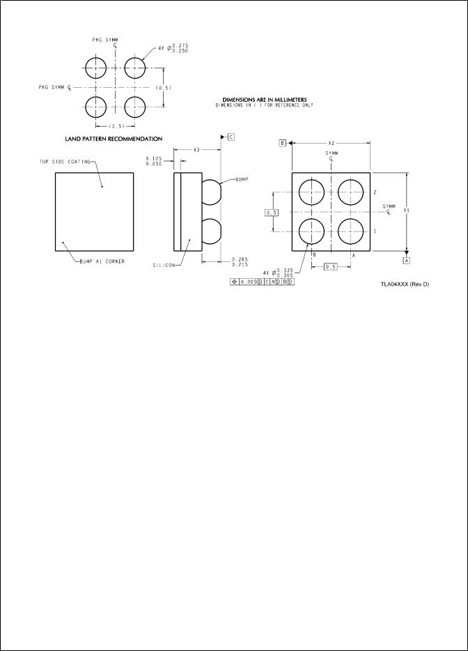
Physical Dimensions inches (millimeters) unless otherwise noted
4-Bump Thin micro SMD
NS Package Number TLA04CDA
The dimensions for X1, X2 and X3 are given as: X1 = 1.065 mm ± 0.030 mm
X2 = 1.090 mm ± 0.030 mm
X3 = 0.600 mm ± 0.075 mm
www.national.com |
10 |