

Розрахункова СЗіВІ / Розрахункова робота / Стабілізатори напруги / LDO National Semiconductor / LP5952
.pdfPower Supply Rejection Ratio VIN, 1.5V Option
20208520
Application Hints
DUAL RAIL SUPPLY
The LP5952 requires two different supply voltages:
•VIN, the power input voltage, is regulated to the fixed output voltage
•VBATT, the bias input voltage, supplies internal circuitry.
It's important that VIN does not exceed VBATT at any time. If the device is used in the typical post regulation application as
shown in Figure 1, the sequencing of the two power supplies
is not an issue as VBATT supplies both, the DC-DC regulator and the LP5952. The output voltage of the DC-DC regulator
will take some time to rise up and supply VIN of LP5952. In this application VIN will always ramp up more slowly than
VBATT.
In case VIN is shorted to VBATT, the voltages at the two supply pins will ramp up simultaneously causing no problem.
Only in applications with two independent supplies connected to the LP5952 special care must be taken to guarantee that VIN is always ≤ VBATT.
POWER DISSIPATION AND DEVICE OPERATION
The permissible power dissipation for any package is a measure of the capability of the device to pass heat from the power source, the junctions of the IC, to the ultimate heat sink, the ambient environment. Thus the power dissipation is dependent on the ambient temperature and the thermal resistance across the various interfaces between the die and ambient air.
As stated in the electrical specification section, the allowable power dissipation for the device in a given package can be calculated using the equation:
PD = (TJ(MAX) - TA) / θJA
With a θJA = 95°C/W, the device in the 5 bump micro SMD package returns a value of 1053mW with a maximum junction temperature of 125°C at TA of 25°C or 421mW at TA of 85°C.
The actual power dissipation across the device can be estimated by the following equation:
PD = (VIN - VOUT) * IOUT
Power Supply Rejection Ratio VBATT, 1.5V Option
20208521
This establishes the relationship between the power dissipation allowed due to thermal consideration, the voltage drop across the device, and the continuous current capability of the device. These two equations should be used to determine the optimum operating conditions for the device in the application. As an example, to keep full load current capability of 350mA for a 1.5V output voltage option at a high ambient temperature of 85°C, VIN has to be kept ≤2.7V (for micro SMD package):
VIN ≤ PD / IOUT + VOUT = 421mW / 350mA + 1.5V = 2.7V. Figure 3 shows the output current derating due to these considerations:
20208525
FIGURE 3. Maximum Load Current vs VIN - VOUT, TA =
85°C, VOUT = 1.5V, θJA(MICROSMD) = 95°C/W,
θJA(LLP) = 150°C/W,
The typical contribution of the bias input voltage supply VBATT to the power dissipation can be neglected:
PD_VBATT = VBATT * IQVBATT = 5.5V * 50µA = 0.275mW typical.
EXTERNAL CAPACITORS
As is common with most regulators, the LP5952 requires external capacitors to ensure stable operation. The LP5952 is specifically designed for portable applications requiring minimum board space and the smallest size components. These capacitors must be correctly selected for good performance.
LP5952
11 |
www.national.com |
LP5952
INPUT CAPACITOR
If the LP5952 is used stand alone, an input capacitor at VIN is required for stability. It is recommended that a 1.0µF capacitor be connected between the LP5952 power voltage input pin VIN and ground (this capacitance value may be increased without limit).
This capacitor must be located a distance of not more than 1 cm from the VIN pin and returned to a clean analogue ground. Any good quality ceramic, tantalum, or film capacitor may be used at the input.
A capacitor at VBATT is not required if the distance to the supply does not exceed 5cm.
If the device is used in the typical application as post regulator after a DC-DC regulator, no input capacitors are required at
all as the capacitors of the DC-DC regulator (CIN and COUT) are sufficient if both components are mounted close to each
other and a proper GND plane is used. If the distance between the output capacitor of the DC-DC regulator and the VIN pin of the LP5952 is larger than 5cm, it's recommended to add the mentioned input capacitor at VIN.
Important: Tantalum capacitors can suffer catastrophic failures due to surge current when connected to a lowimpedance source of power (like a battery or a very large capacitor). If a tantalum capacitor is used at the input, it must be guaranteed by the manufacturer to have a surge current rating sufficient for the application.
The ESR (Equivalent Series Resistance) of the input capacitor should be in the range of 3mΩ to 300mΩ. The tolerance and temperature coefficient must be considered when selecting the capacitor to ensure the capacitance will remain ≥ 470nF over the entire operating temperature range.
OUTPUT CAPACITOR
The LP5952 is designed specifically to work with very small ceramic output capacitors. A ceramic capacitor (dielectric types X7R, Z5U, or Y5V) in the 2.2µF range (up to 10µF) and
with an ESR between 3mΩ to 300mΩ is suitable as COUT in the LP5952 application circuit.
This capacitor must be located a distance of not more than
1cm from the VOUT pin and returned to a clean analogue ground.
It is also possible to use tantalum or film capacitors at the
device output, VOUT, but these are not as attractive for reasons of size and cost (see the section Capacitor Character-
istics).
CAPACITOR CHARACTERISTICS
The LP5952 is designed to work with ceramic capacitors on the output to take advantage of the benefits they offer. For capacitance values in the range of 1µF to 4.7µF, ceramic capacitors are the smallest, least expensive and have the lowest ESR values, thus making them best for eliminating high frequency noise. The ESR of a typical 1µF ceramic capacitor is in the range of 3mΩ to 40mΩ, which easily meets the ESR requirement for stability for the LP5952.
For both input and output capacitors, careful interpretation of the capacitor specification is required to ensure correct device operation. The capacitor value can change greatly, depending on the operating conditions and capacitor type.
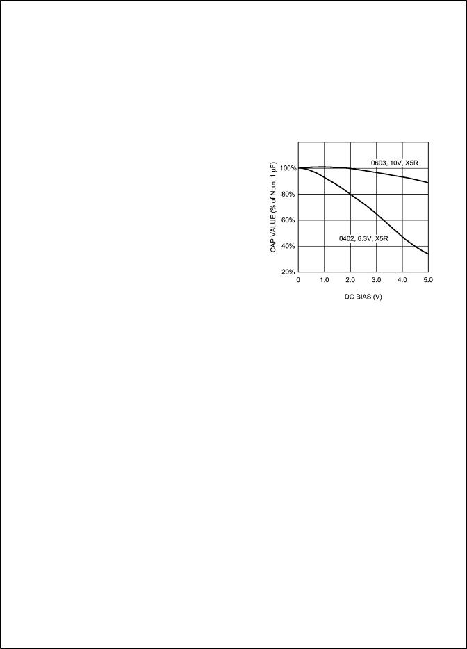
In particular, the output capacitor selection should take account of all the capacitor parameters, to ensure that the specification is met within the application. The capacitance can vary with DC bias conditions as well as temperature and frequency of operation. Capacitor values will also show some decrease over time due to aging. The capacitor parameters
are also dependant on the particular case size, with smaller sizes giving poorer performance figures in general. The example shows a typical graph comparing different capacitor case sizes in a Capacitance vs. DC Bias plot. As shown in the graph, increasing the DC Bias condition can result in the capacitance value falling below the minimum value given in the recommended capacitor specifications table (0.47/1.5µF in this case). Note that the graph shows the capacitance out of spec for the 0402 case size capacitor at higher bias voltages. It is therefore recommended that the capacitor manufacturers’ specifications for the nominal value capacitor are consulted for all conditions, as some capacitor sizes (e.g. 0402) may not be suitable in the actual application.
20208507
FIGURE 4. Graph Showing A Typical Variation In Capacitance vs DC Bias
The ceramic capacitor’s capacitance can vary with temperature. The capacitor type X7R, which operates over a temperature range of -55°C to +125°C, will only vary the capacitance to within ±15%. The capacitor type X5R has a similar tolerance over a reduced temperature range of -55°C to +85°C. Many large value ceramic capacitors, larger than 1µF are manufactured with Z5U or Y5V temperature characteristics. Their capacitance can drop by more than 50% as the temperature varies from 25°C to 85°C. Therefore X7R is recommended over Z5U and Y5V in applications where the ambient temperature will change significantly above or below 25°C.
Tantalum capacitors are less desirable than ceramic for use as output capacitors because they are more expensive when comparing equivalent capacitance and voltage ratings in the 1µF to 4.7µF range.
Another important consideration is that tantalum capacitors have higher ESR values than equivalent size ceramics. This means that while it may be possible to find a tantalum capacitor with an ESR value within the stable range, it would have to be larger in capacitance (which means bigger and more costly) than a ceramic capacitor with the same ESR value. It should also be noted that the ESR of a typical tantalum will increase about 2:1 as the temperature goes from 25°C down to -40°C, so some guard band must be allowed.
NO-LOAD STABILITY
The LP5952 will remain stable and in regulation with no external load. This is an important consideration in some circuits, for example CMOS RAM keep-alive applications.
www.national.com |
12 |

ENABLE OPERATION
The LP5952 may be switched ON or OFF by a logic input at the Enable pin, VEN. A logic high at this pin will turn the device on. When the enable pin is low, the regulator output is off and the device typically consumes 0.1µA.
If the application does not require the Enable switching fea-
ture, the VEN pin should be tied to VBATT to keep the regulator output permanently on.
To ensure proper operation, the signal source used to drive the VEN input must be able to swing above and below the specified turn-on/off voltage thresholds listed in the Electrical Characteristics section under Enable Control Characteristics, VIL and VIH.
FAST TURN ON
Fast turn-on is guaranteed by an optimized architecture allowing a fast ramp of the output voltage to reach the target voltage while the inrush current is controlled low at 120mA typical (for a COUT of 2.2µF).
SHORT-CIRCUIT PROTECTION
The LP5952 is short circuit protected and in the event of a peak over-current condition, the output current through the NFET pass device will be limited.
If the over-current condition exists for a longer time, the average power dissipation will increase depending on the input to output voltage difference until the thermal shutdown circuitry will turn off the NFET.
Please refer to the section on thermal information for power dissipation calculations.
THERMAL-OVERLOAD PROTECTION
Thermal-Overload Protection limits the total power dissipation in the LP5952. When the junction temperature exceeds TJ =
165°C typ., the shutdown logic is triggered and the NFET is turned off, allowing the device to cool down. After the junction temperature dropped by 20°C (temperature hysteresis) typical, the NFET is activated again. This results in a pulsed output voltage during continuous thermal-overload conditions.
The Thermal-Overload Protection is designed to protect the LP5952 in the event of a fault condition. For normal, continuous operation, do not exceed the absolute maximum junction temperature rating of TJ = +150°C (see Absolute Maximum Ratings).
REVERSE CURRENT PATH
The internal NFET pass device in LP5952 has an inherent parasitic body diode. During normal operation, the input voltage is higher than the output voltage and the parasitic diode is reverse biased. However, if the output is pulled above the input in an application, then current flows from the output to the input as the parasitic diode gets forward biased. The output can be pulled above the input as long as the current in the parasitic diode is limited to 50mA. For currents above this limit an external Schottky diode must be connected from VOUT to VIN (cathode on VIN, anode on VOUT).
EVALUATION BOARDS
For availability of evaluation boards please refer to the Product Folder of LP5952 at www.national.com.
For information regarding evaluation boards, please refer to Application Note: AN-1531.
LP5952
13 |
www.national.com |

LP5952
Physical Dimensions inches (millimeters) unless otherwise noted
NS Package Number TLA05Z1A X1 = 955 µm ±30µm
X2 = 1335µm ±30µm
X3 = 600µm ±75µm
5-Bump Thin Micro SMD Package, Large Bump
NS Package Number LCA06B
6-Pin Chip On Lead LLP Package, 0.5mm Pitch
For most accurate revision please refer to www.national.com/packaging/parts/
www.national.com |
14 |

Notes
LP5952
15 |
www.national.com |

LP5952 350mA Dual Rail Linear Regulator
Notes
For more National Semiconductor product information and proven design tools, visit the following Web sites at:
Products |
Design Support |
||
|
|
|
|
Amplifiers |
www.national.com/amplifiers |
WEBENCH |
www.national.com/webench |
|
|
|
|
Audio |
www.national.com/audio |
Analog University |
www.national.com/AU |
|
|
|
|
Clock Conditioners |
www.national.com/timing |
App Notes |
www.national.com/appnotes |
|
|
|
|
Data Converters |
www.national.com/adc |
Distributors |
www.national.com/contacts |
|
|
|
|
Displays |
www.national.com/displays |
Green Compliance |
www.national.com/quality/green |
|
|
|
|
Ethernet |
www.national.com/ethernet |
Packaging |
www.national.com/packaging |
|
|
|
|
Interface |
www.national.com/interface |
Quality and Reliability |
www.national.com/quality |
|
|
|
|
LVDS |
www.national.com/lvds |
Reference Designs |
www.national.com/refdesigns |
|
|
|
|
Power Management |
www.national.com/power |
Feedback |
www.national.com/feedback |
|
|
|
|
Switching Regulators |
www.national.com/switchers |
|
|
|
|
|
|
LDOs |
www.national.com/ldo |
|
|
|
|
|
|
LED Lighting |
www.national.com/led |
|
|
|
|
|
|
PowerWise |
www.national.com/powerwise |
|
|
|
|
|
|
Serial Digital Interface (SDI) |
www.national.com/sdi |
|
|
|
|
|
|
Temperature Sensors |
www.national.com/tempsensors |
|
|
|
|
|
|
Wireless (PLL/VCO) |
www.national.com/wireless |
|
|
|
|
|
|
|
|
|
|
THE CONTENTS OF THIS DOCUMENT ARE PROVIDED IN CONNECTION WITH NATIONAL SEMICONDUCTOR CORPORATION (“NATIONAL”) PRODUCTS. NATIONAL MAKES NO REPRESENTATIONS OR WARRANTIES WITH RESPECT TO THE ACCURACY OR COMPLETENESS OF THE CONTENTS OF THIS PUBLICATION AND RESERVES THE RIGHT TO MAKE CHANGES TO SPECIFICATIONS AND PRODUCT DESCRIPTIONS AT ANY TIME WITHOUT NOTICE. NO LICENSE, WHETHER EXPRESS, IMPLIED, ARISING BY ESTOPPEL OR OTHERWISE, TO ANY INTELLECTUAL PROPERTY RIGHTS IS GRANTED BY THIS DOCUMENT.
TESTING AND OTHER QUALITY CONTROLS ARE USED TO THE EXTENT NATIONAL DEEMS NECESSARY TO SUPPORT NATIONAL’S PRODUCT WARRANTY. EXCEPT WHERE MANDATED BY GOVERNMENT REQUIREMENTS, TESTING OF ALL PARAMETERS OF EACH PRODUCT IS NOT NECESSARILY PERFORMED. NATIONAL ASSUMES NO LIABILITY FOR APPLICATIONS ASSISTANCE OR BUYER PRODUCT DESIGN. BUYERS ARE RESPONSIBLE FOR THEIR PRODUCTS AND APPLICATIONS USING NATIONAL COMPONENTS. PRIOR TO USING OR DISTRIBUTING ANY PRODUCTS THAT INCLUDE NATIONAL COMPONENTS, BUYERS SHOULD PROVIDE ADEQUATE DESIGN, TESTING AND OPERATING SAFEGUARDS.
EXCEPT AS PROVIDED IN NATIONAL’S TERMS AND CONDITIONS OF SALE FOR SUCH PRODUCTS, NATIONAL ASSUMES NO LIABILITY WHATSOEVER, AND NATIONAL DISCLAIMS ANY EXPRESS OR IMPLIED WARRANTY RELATING TO THE SALE AND/OR USE OF NATIONAL PRODUCTS INCLUDING LIABILITY OR WARRANTIES RELATING TO FITNESS FOR A PARTICULAR PURPOSE, MERCHANTABILITY, OR INFRINGEMENT OF ANY PATENT, COPYRIGHT OR OTHER INTELLECTUAL PROPERTY RIGHT.
LIFE SUPPORT POLICY
NATIONAL’S PRODUCTS ARE NOT AUTHORIZED FOR USE AS CRITICAL COMPONENTS IN LIFE SUPPORT DEVICES OR SYSTEMS WITHOUT THE EXPRESS PRIOR WRITTEN APPROVAL OF THE CHIEF EXECUTIVE OFFICER AND GENERAL COUNSEL OF NATIONAL SEMICONDUCTOR CORPORATION. As used herein:
Life support devices or systems are devices which (a) are intended for surgical implant into the body, or (b) support or sustain life and whose failure to perform when properly used in accordance with instructions for use provided in the labeling can be reasonably expected to result in a significant injury to the user. A critical component is any component in a life support device or system whose failure to perform can be reasonably expected to cause the failure of the life support device or system or to affect its safety or effectiveness.
National Semiconductor and the National Semiconductor logo are registered trademarks of National Semiconductor Corporation. All other brand or product names may be trademarks or registered trademarks of their respective holders.
Copyright© 2008 National Semiconductor Corporation
For the most current product information visit us at www.national.com
National Semiconductor |
National Semiconductor Europe |
National Semiconductor Asia |
National Semiconductor Japan |
Americas Technical |
Technical Support Center |
Pacific Technical Support Center |
Technical Support Center |
Support Center |
Email: europe.support@nsc.com |
Email: ap.support@nsc.com |
Email: jpn.feedback@nsc.com |
Email: support@nsc.com |
German Tel: +49 (0) 180 5010 771 |
|
|
Tel: 1-800-272-9959 |
English Tel: +44 (0) 870 850 4288 |
|
|
www.national.com