

Розрахункова СЗіВІ / Розрахункова робота / Стабілізатори напруги / LDO National Semiconductor / LP5952
.pdfJune 10, 2008
LP5952
350mA Dual Rail Linear Regulator
General Description
The LP5952 is a Dual Supply Rail Linear Regulator optimized for powering ultra-low voltage circuits from a single Li-Ion cell or 3 cell NiMH/NiCd batteries.
In the typical post regulation application VBATT is directly connected to the battery (range 2.5V...5.5V) and VIN is supplied by the output voltage of the DC-DC Converter (range 0.7V...
4.5V).
The device offers superior dropout and transient features combined with very low quiescent currents. In shutdown mode (Enable pin pulled low) the device turns off and reduces battery consumption to 0.1µA (typ.).
The LP5952 also features internal protection against overtemperature, over-current and under-voltage conditions.
Performance is specified for a -40°C to 125°C junction temperature range.
The device is available in a tiny 5-bump micro SMD and a 6- pin Chip On Lead LLP package, lead free.
The device is available in fixed output voltages in the range of 0.5V to 2.0V. For availability, please contact your local NSC sales office.
Features
■Excellent load transient response: ±15mV typical
■Excellent line transient response: ±1mV typical
■0.7V ≤ VIN ≤ 4.5V
■2.5V ≤ VBATT ≤ 5.5V
■0.5V ≤ VOUT ≤ 2.0V
■For ILOAD = 350mA:
VBATT ≥ VOUT(NOM) + 1.5V or 2.5V whichever is higher
■For ILOAD = 150mA:
VBATT ≥ VOUT(NOM) + 1.3V or 2.5V whichever is higher
■50µA typical quiescent current from VBATT
■10µA typical quiescent current from VIN
■0.1µA typical quiescent current in shutdown
■Guaranteed 350mA output current
■Noise voltage = 100µVRMS typical
■Operates from a single Li-Ion cell or 3 cell NiMH/NiCd batteries
■Only one or two tiny surface-mount external components required depending on application
■Small, thin 5-bump micro SMD package and 6-pin Chip On Lead LLP package, lead free
■Thermal-overload and short-circuit protection
■-40°C to +125°C junction temperature range
Applications
■ Mobile Phones
■ Hand-Held Radios
■ Personal Digital Assistants
■ Palm-Top PCs
■ Portable Instruments
■ Battery Powered Devices
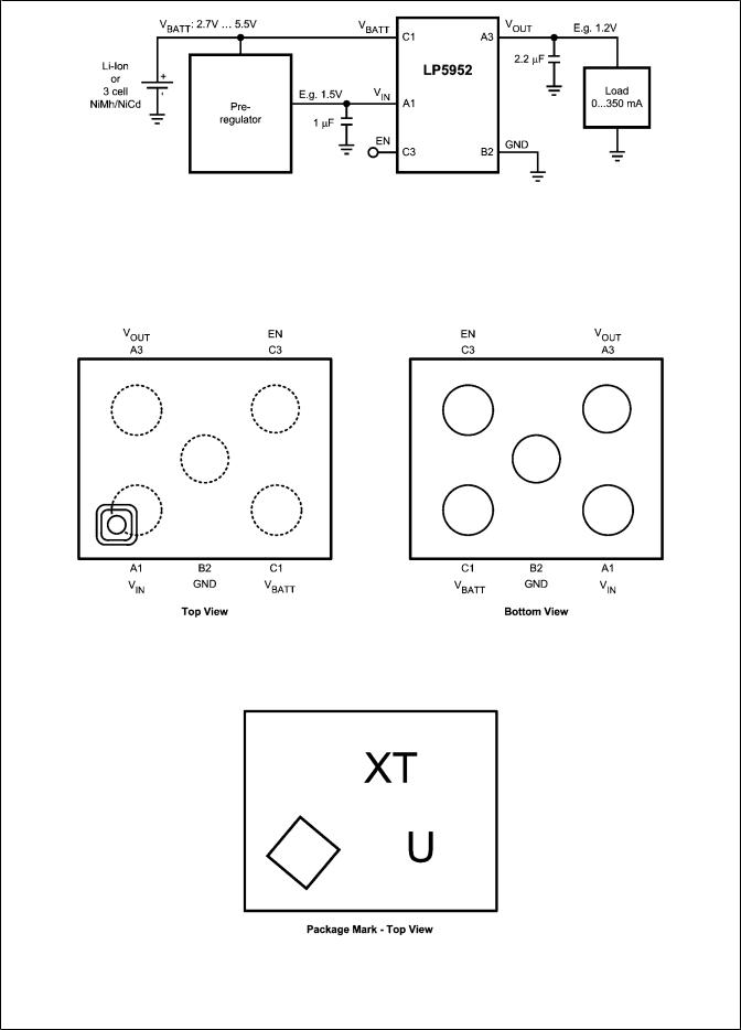
Typical Application Circuit
20208501
FIGURE 1. Typical Application Circuit with DC-DC Converter as Pre-Regulator for VIN
Regulator Linear Rail Dual 350mA LP5952
© 2008 National Semiconductor Corporation |
202085 |
www.national.com |
LP5952
20208502
FIGURE 2. Typical Application Circuit
Connection Diagrams
5-Bump Micro SMD Package
20208503
Connection Diagram 5-Bump Thin Micro SMD Package, Large Bump, 0.5mm Pitch
See NS Package Number TLA05
Package Marking
20208506
www.national.com |
2 |

LLP-6 Package
20208524
Connection Diagram 6-Pin Chip On Lead LLP package, 0.5mm pitch See NS Package Number LCA06B
Note: The actual physical placement of the package marking will vary from part to part. The package marking “X” designates the date code. “T” is a NSC internal code for die traceability. Both will vary considerably. “U” identifies the device (part number, option, etc.).
Pin Descriptions
Pin Number |
Pin Number |
Pin Name |
Description |
|
Micro SMD |
LLP |
|
|
|
A1 |
3 |
VIN |
Power input voltage; input range: 0.7V to 4.5V, VIN ≤ VBATT |
|
A3 |
4 |
VOUT |
Regulated output voltage |
|
B2 |
2 |
GND |
Ground |
|
C1 |
1 |
VBATT |
Bias input voltage; input range: 2.5V to 5.5V |
|
C3 |
6 |
EN |
Enable pin logic input: low = shutdown, high = active, normal operation. |
|
This pin should not be left floating. Tie to VBATT if this function is not used. |
||||
|
|
|
||
|
5 |
NC |
Do not make connections to this pin |
|
|
|
|
|
Order Information (5-bump micro SMD)
Output Voltage |
LP5952 Supplied as 250 Units, |
LP5952 Supplied as 3000 Units, |
Flow |
Package |
|
(V) |
Tape and Reel, lead free |
Tape and Reel, lead free |
Marking |
||
|
|||||
0.7 |
LP5952TL-0.7 |
LP5952TLX-0.7 |
NOPB |
4 |
|
|
|
|
|
|
|
1.0 |
LP5952TL-1.0 |
LP5952TLX-1.0 |
NOPB |
L |
|
1.2 |
LP5952TL-1.2 |
LP5952TLX-1.2 |
NOPB |
7 |
|
|
|
|
|
|
|
1.3 |
LP5952TL-1.3 |
LP5952TLX-1.3 |
NOPB |
U |
|
|
|
|
|
|
|
1.4 |
LP5952TL-1.4 |
LP5952TLX-1.4 |
NOPB |
A |
|
1.5 |
LP5952TL-1.5 |
LP5952TLX-1.5 |
NOPB |
T |
|
|
|
|
|
|
|
1.6 |
LP5952TL-1.6 |
LP5952TLX-1.6 |
NOPB |
B |
|
|
|
|
|
|
|
1.8 |
LP5952TL-1.8 |
LP5952TLX-1.8 |
NOPB |
8 |
|
2.0 |
LP5952TL-2.0 |
LP5952TLX-2.0 |
NOPB |
5 |
|
|
|
|
|
|
LP5952
3 |
www.national.com |

LP5952
Order Information (COL LLP-6)
Output Voltage |
LP5952 Supplied as 1000 Units, |
LP5952 Supplied as 4500 Units, |
Flow |
Package |
(V) |
Tape and Reel, lead free |
Tape and Reel, lead free |
|
Marking |
1.2 |
LP5952LC-1.2 |
LP5952LCX-1.2 |
NOPB |
L28 |
|
|
|
|
|
1.3 |
LP5952LC-1.3 |
LP5952LCX-1.3 |
NOPB |
L43 |
1.5 |
LP5952LC-1.5 |
LP5952LCX-1.5 |
NOPB |
L25 |
|
|
|
|
|
1.8 |
LP5952LC-1.8 |
LP5952LCX-1.8 |
NOPB |
L29 |
|
|
|
|
|
www.national.com |
4 |

Absolute Maximum Ratings (Notes 1, 2)
If Military/Aerospace specified devices are required, please contact the National Semiconductor Sales Office/ Distributors for availability and specifications.
VIN, VBATT pins: Voltage to GND, |
|
VIN ≤ VBATT: |
-0.2V to 6.0V |
VBATT pin to VIN pin: |
0.2V |
EN pin, Voltage to GND: |
-0.2V to 6.0V |
Continuous Power Dissipation |
|
(Note 3): |
Internally Limited |
Junction Temperature (TJ-MAX ): |
150°C |
Storage Temperature Range: |
-65°C to + 150°C |
Package Peak Reflow Temperature |
|
(Pb-free, 10-20 sec.) (Note 4): |
260°C |
ESD Rating (Note 5): |
|
Human Body Model: |
2.0kV |
Machine Model: |
200V |
Operating Ratings
Input Voltage Range VIN |
0.7V to 4.5V |
Input Voltage Range V |
2.5V to 5.5V |
BATT |
|
VEN Input Voltage |
0 to VBATT |
Recommended Load Current |
0mA to 350mA |
Junction Temperature (TJ) Range |
-40°C to + 125°C |
Ambient Temperature (TA) Range |
|
(Note 6) |
-40°C to + 85°C |
Thermal Properties
Junction-to-Ambient Thermal |
|
Resistance (θJA) |
|
TLA05 package (Note 7) |
95°C/W |
LCA06B package (Note 7) |
150°C/W |
ESD Caution Notice
National Semiconductor recommends that all integrated circuits be handled with appropriate precautions. Failure to observe proper ESD handling techniques can result in damage.
Electrical Characteristics (Notes 2, 8, 11)
Typical values and limits appearing in standard typeface are for TA = 25°C. Limits appearing in boldface type apply over the full operating temperature range: -40°C ≤ TJ ≤ +125°C. Unless otherwise noted, specifications apply to the typical application circuit with VIN = VOUT(NOM) + 1.0V, VBATT = VOUT(NOM) + 1.5V or 2.5V, whichever is higher, IOUT = 1mA, CVIN = 1.0µF, COUT = 2.2µF,
VEN = VBATT.
Symbol |
Parameter |
Condition |
|
Typ |
Limit |
Units |
||
|
Min |
Max |
||||||
|
|
|
|
|
|
|
||
VOUT / VOUT |
Output Voltage Tolerance |
VIN = VOUT(NOM) + 0.3V |
|
|
-1.5 |
1.5 |
% |
|
|
|
-2.0 |
2.0 |
% |
||||
|
|
|
|
|
|
|||
VOUT / |
VIN |
|
VIN = VOUT(NOM) + 0.3V to 4.5V, VBATT = |
0.3 |
|
1.0 |
mV/V |
|
Line Regulation Error |
4.5V |
|
|
|
|
|
||
|
|
|
|
|
|
|
||
VOUT / |
VBATT |
|
VBATT = VOUT(NOM) + 1.5V (≥2.5V) to 5.5V |
0.5 |
|
2.2 |
|
|
|
|
|
IOUT = 1mA to 350mA, micro SMD |
15 |
|
30 |
µV/mA |
|
VOUT / |
mA |
Load Regulation Error |
package |
|
|
|||
|
|
|
|
|
||||
|
|
|
IOUT = 1mA to 350mA, LLP-6 package |
43 |
|
60 |
µV/mA |
|
ISC |
|
Output Current |
VOUT = 0V, VEN = VIN = VBATT = VOUT |
500 |
350 |
|
mA |
|
|
(short circuit) |
(NOM) + 1.5V |
|
|
||||
|
|
|
|
|
|
|
||
|
|
|
IOUT = 350mA, VIN = VOUT(NOM) |
+ 0.3V, |
1.07 |
|
1.5 |
V |
|
|
|
micro SMD package |
|
|
|||
|
|
|
|
|
|
|
|
|
|
|
|
IOUT = 350mA, VIN = VOUT(NOM) |
+ 0.3V, |
1.08 |
|
1.5 |
V |
VDO_VBATT |
Output Voltage Dropout VBATT |
LLP-6 package |
|
|
||||
|
|
|
|
|
||||
(Note 10) |
|
(Note 9) |
IOUT = 150mA, VIN = VOUT(NOM) |
+ 0.3V, |
0.96 |
|
1.3 |
V |
|
|
|
micro SMD package |
|
|
|||
|
|
|
|
|
|
|
|
|
|
|
|
IOUT = 150mA, VIN = VOUT(NOM) |
+ 0.3V, |
0.97 |
|
1.3 |
V |
|
|
|
LLP-6 package |
|
|
|||
|
|
|
|
|
|
|
|
|
|
|
|
IOUT = 350mA, VBATT = VOUT(NOM) + 1.5V |
88 |
|
200 |
mV |
|
|
|
|
or 2.5V, micro SMD package |
|
|
|||
VDO_VIN |
|
Output Voltage Dropout VIN |
|
|
|
|
|
|
|
IOUT = 350mA, VBATT = VOUT(NOM) + 1.5V |
128 |
|
250 |
mV |
|||
|
|
|
|
|||||
|
|
|
or 2.5V, LLP-6 package |
|
|
|||
|
|
|
|
|
|
|
|
|
|
|
|
|
|
|
|
|
|
EN |
|
Output Noise |
10Hz to 100kHz |
|
100 |
|
|
µVRMS |
LP5952
5 |
www.national.com |

LP5952 |
|
|
|
|
|
|
|
|
|
Symbol |
Parameter |
Condition |
Typ |
Limit |
Units |
|
|||
|
|
|
|||||||
|
|
Min |
Max |
|
|||||
|
|
|
|
|
|
|
|
||
|
|
|
|
Sine modulated VBATT |
|
|
|
|
|
|
|
|
|
f = 10Hz |
70 |
|
|
dB |
|
|
|
|
|
f = 100Hz |
65 |
|
|
dB |
|
|
|
|
|
f = 1kHz |
45 |
|
|
dB |
|
|
|
|
|
|
|
|
|
|
|
|
|
PSRR |
Power Supply Rejection Ratio |
Sine modulated VIN |
|
|
|
|
|
|
|
|
|
f = 10Hz |
80 |
|
|
dB |
|
|
|
|
|
f = 100Hz |
90 |
|
|
dB |
|
|
|
|
|
f = 1kHz |
95 |
|
|
dB |
|
|
|
|
|
f = 10kHz |
85 |
|
|
dB |
|
|
|
|
|
f = 100kHz |
64 |
|
|
dB |
|
|
|
|
|
|
|
|
|
|
|
Quiescent Currents
Symbol |
Parameter |
Condition |
Typ |
Limit |
Units |
||
Min |
Max |
||||||
|
|
|
|
|
|||
IQ_VBATT |
Current into VBATT |
ILOAD = 0...350mA |
50 |
|
100 |
µA |
|
IQ_VIN |
Current into VIN |
ILOAD = 0 |
11 |
|
28 |
µA |
|
Shutdown Currents
Symbol |
Parameter |
Condition |
Typ |
Limit |
Units |
||
Min |
Max |
||||||
|
|
|
|
|
|||
IQ_VBATT |
Current into VBATT |
VEN = 0V |
0.1 |
|
1 |
µA |
|
IQ_VIN |
Current into VIN |
VEN = 0V |
0.1 |
|
1 |
µA |
|
Enable Control Characteristics
Symbol |
Parameter |
Conditions |
Typ |
Limit |
Units |
||
Min |
Max |
||||||
|
|
|
|
|
|||
IEN |
Maximum Input Current at VEN |
|
0.01 |
|
1 |
µA |
|
Input |
|
|
|||||
|
|
|
|
|
|
||
|
|
|
|
|
|
|
|
VIL |
Low Input Threshold (shutdown) |
|
|
|
0.4 |
V |
|
VIH |
High Input Threshold (enable) |
|
|
1.0 |
|
V |
|
Thermal Protection
Symbol |
Parameter |
Conditions |
Typ |
Limit |
Units |
||
Min |
Max |
||||||
|
|
|
|
|
|||
TSHDN |
Thermal-Shutdown Temperature |
|
165 |
|
|
°C |
|
TSHDN |
Thermal-Shutdown Hysteresis |
|
20 |
|
|
°C |
|
www.national.com |
6 |

Transient Characteristics
Symbol |
Parameter |
Conditions |
Typ |
Limit |
Units |
||
Min |
Max |
||||||
|
|
|
|
|
|||
VOUT |
Dynamic Line Transient |
VIN = VOUT(NOM) + 0.3V to |
±1 |
|
|
mV |
|
Response VIN |
VOUT(NOM) + 0.9V; tr, tf = 10µs |
|
|
||||
|
|
|
|
|
|||
VOUT |
Dynamic Line Transient |
VBATT = VOUT(NOM) + 1.5V to |
±15 |
|
|
mV |
|
Response VBATT |
VOUT(NOM) + 2.1V; tr, tf = 10µs |
|
|
||||
|
|
|
|
|
|||
|
Dynamic Load Transient |
Pulsed load 0 ...300mA, di/dt = 300mA/ |
|
|
|
|
|
|
Response |
1µs |
±15 |
|
|
mV |
|
VOUT |
|
micro SMD package |
|
|
|
|
|
|
|
|
|
|
|
||
|
Pulsed load 0 ...300mA, di/dt = 300mA/ |
-35/ |
|
|
|
||
|
|
|
|
|
|||
|
|
1µs |
|
|
mV |
||
|
|
+15 |
|
|
|||
|
|
LLP-6 package |
|
|
|
||
|
|
|
|
|
|
||
|
|
|
|
|
|
|
|
TSTARTUP |
Startup Time |
EN to 0.95 * VOUT |
70 |
|
150 |
µs |
|
Input and Output Capacitors, Recommended Specification
Symbol |
Parameter |
Conditions |
Nom |
Limit |
Units |
||
Min |
Max |
||||||
|
|
|
|
|
|||
COUT |
Output Capacitance |
Capacitance (Note 12) |
2.2 |
1.5 |
10 |
µF |
|
|
|
|
|
|
|||
ESR |
|
3 |
300 |
mΩ |
|||
|
|
|
|||||
|
|
Capacitance (Note 12), not needed in typ |
|
|
|
|
|
CVIN |
Input Capacitance at VIN |
post regulation application, |
1 |
0.47 |
|
µF |
|
see Figure 1 |
|
|
|
|
|||
|
|
ESR |
|
3 |
300 |
mΩ |
|
Note 1: Absolute Maximum Ratings indicate limits beyond which damage to the component may occur. Operating Ratings are conditions under which operation of the device is guaranteed. Operating Ratings do not imply guaranteed performance limits. For guaranteed performance limits and associated test conditions, see the Electrical Characteristics tables.
Note 2: All voltages are with respect to the potential at the GND pin.
Note 3: Internal thermal shutdown circuitry protects the device from permanent damage. Thermal shutdown engages at TJ = 165°C (typ.) and disengages at TJ = 145°C (typ.).
Note 4: For detailed soldering specifications and information, please refer to National Semiconductor Application Note 1112: Micro SMD Wafer Level Chip Scale Package (AN-1112) and Application Note 1187: Leadless Leadframe Package (LLP) (AN-1187).
Note 5: The Human body model is a 100pF capacitor discharged through a 1.5kΩ resistor into each pin. The machine model is a 200pF capacitor discharged directly into each pin. (MIL-STD-883 3015.7)
Note 6: In applications where high power dissipation and/or poor package thermal resistance is present, the maximum ambient temperature may have to be derated. Maximum ambient temperature (TA-MAX) is dependent on the maximum operating junction temperature (TJ-MAX-OP = 125°C), the maximum power dissipation of the device in the application (PD-MAX), and the junction-to ambient thermal resistance of the part/package in the application (θJA), as given by the following equation: TA-MAX = TJ-MAX-OP – (θJA × PD-MAX).
Note 7: Junction-to-ambient thermal resistance is highly application and board-layout dependent. In applications where high maximum power dissipation exists, special attention must be paid to thermal dissipation issues in board design.
Note 8: Min and Max limits are guaranteed by design, test, or statistical analysis. Typical (Typ) numbers are not guaranteed, but do represent the most likely
norm. Unless otherwise specified, conditions for Typ specifications are: VIN = VOUT(NOM) + 1.0V, VBATT= VOUT(NOM) + 1.5V or 2.5V, whichever is higher, TA = 25° C.
Note 9: Dropout voltage is defined as the input to output voltage differential at which the output voltage falls to 100mV below the nominal output voltage.
Note 10: This specification does not apply if the battery voltage VBATT needs to be decreased below the minimum operating limit of 2.5V during this test.
Note 11: VOUT(NOM) is the stated output voltage option
Note 12: The capacitor tolerance should be 30% or better over temperature. The full operating conditions for the application should be considered when selecting a suitable capacitor to ensure that the minimum value of capacitance is always met. Recommended capacitor type is X7R. However, dependent on application, X5R, Y5V, and Z5U can also be used. The shown minimum limit represents real minimum capacitance, including all tolerances and must be maintained over temperature and dc bias voltage (See capacitor section in Applications Hints)
LP5952
7 |
www.national.com |

LP5952
Block Diagram
20208505
www.national.com |
8 |

Typical Performance Characteristics Unless otherwise specified, CIN = 1.0µF ceramic, COUT = 2.2µF ceramic, VIN = VOUT(NOM) + 1V, VBATT = VOUT(NOM) + 1.5V, TA = 25°C, Enable pin is tied to VBATT. Micro SMD package.
Load Transient Response, 0.7V Option |
Load Transient Response, 1.5V Option |
20208509 |
20208510 |
|
|
Line Transient Response VIN, 1.5V Option |
Line Transient Response VBATT, 1.5V Option |
|
20208511 |
20208512 |
|
|
|
Enable Start-up Time, 0.7V Option |
|
Enable Start-up Time, 1.5V Option |
20208513 |
20208514 |
|
LP5952
9 |
www.national.com |

LP5952
Output Voltage Change vs Temperature |
Dropout VIN vs Temperature, ILOAD = 350mA |
20208515
20208516
Inrush Current VIN, 1.5V Option |
Quiescent Current IQ_VBATT vs VBATT |
|
20208517 |
|
20208522 |
Ground Current vs VBATT / VIN |
Ground Current vs Load Current |
20208523
20208519
www.national.com |
10 |