

Розрахункова СЗіВІ / Розрахункова робота / Стабілізатори напруги / LDO National Semiconductor / LP3852
.pdfSeptember 2006
LP3852/LP3855
1.5A Fast Response Ultra Low Dropout Linear
Regulators
General Description
The LP3852/LP3855 series of fast ultra low-dropout linear regulators operate from a +2.5V to +7.0V input supply. Wide range of preset output voltage options are available. These ultra low dropout linear regulators respond very quickly to step changes in load, which makes them suitable for low voltage microprocessor applications. The LP3852/LP3855 are developed on a CMOS process which allows low quiescent current operation independent of output load current. This CMOS process also allows the LP3852/LP3855 to operate under extremely low dropout conditions.
Dropout Voltage: Ultra low dropout voltage; typically 24mV at 150mA load current and 240mV at 1.5A load current.
Ground Pin Current: Typically 4mA at 1.5A load current.
Shutdown Mode: Typically 10nA quiescent current when the shutdown pin is pulled low.
Error Flag: Error flag goes low when the output voltage drops 10% below nominal value.
SENSE: Sense pin improves regulation at remote loads.
Precision Output Voltage: Multiple output voltage options are available ranging from 1.8V to 5.0V with a guaranteed accuracy of ±1.5% at room temperature, and ±3.0% over all conditions (varying line, load, and temperature).
Features
n Ultra low dropout voltage
n Stable with selected ceramic capacitors n Low ground pin current
n Load regulation of 0.06%
n 10nA quiescent current in shutdown mode n Guaranteed output current of 1.5A DC
n Available in TO-263, TO-220 and SOT-223 packages n Output voltage accuracy ± 1.5%
n Error flag indicates output status
n Sense option improves load regulation n Overtemperature/overcurrent protection
n −40˚C to +125˚C junction temperature range
Applications
n Microprocessor power supplies
n GTL, GTL+, BTL, and SSTL bus terminators n Power supplies for DSPs
n SCSI terminator n Post regulators
n High efficiency linear regulators n Battery chargers
n Other battery powered applications
Typical Application Circuits
20031001
**SD and ERROR pins must be pulled high through a 10kΩ pull-up resistor. Connect the ERROR pin to ground if this function is not used. See Application Hints for more information.
Regulators Linear Dropout Low Ultra Response Fast 5A.1 LP3852/LP3855
© 2006 National Semiconductor Corporation |
DS200310 |
www.national.com |

LP3852/LP3855
Typical Application Circuits (Continued)
20031034
**SD must be pulled high through a 10kΩ pull-up resistor. See Application Hints for more information.
Connection Diagrams
20031005 |
20031006 |
Top View |
Top View |
TO220-5 Package |
TO263-5 Package |
Bent, Staggered Leads |
|
20031096
Top View
SOT223-5 Package
www.national.com |
2 |

Pin Descriptions for TO220-5 and TO263-5 Packages
Pin # |
|
|
|
|
|
LP3852 |
|
|
|
LP3855 |
||||
|
|
|
|
|
|
|
|
|
|
|
|
|
|
|
|
Name |
|
|
Function |
Name |
|
Function |
|||||||
|
|
|
|
|
||||||||||
|
|
|
|
|
|
|
|
|
|
|
|
|
|
|
1 |
|
|
|
|
|
Shutdown |
|
|
|
|
Shutdown |
|||
|
|
SD |
|
|
|
|
SD |
|
|
|||||
|
|
|
|
|
|
|
|
|
|
|
|
|
|
|
2 |
|
VIN |
|
Input Supply |
VIN |
|
Input Supply |
|||||||
3 |
|
GND |
|
Ground |
GND |
|
Ground |
|||||||
|
|
|
|
|
|
|
|
|
|
|
|
|
|
|
4 |
|
VOUT |
|
Output Voltage |
VOUT |
|
Output Voltage |
|||||||
5 |
|
|
|
|
Flag |
SENSE |
|
Remote Sense Pin |
||||||
|
ERROR |
|
|
|
ERROR |
|
||||||||
|
|
|
|
|
|
|
|
|
|
|
|
|
|
|
Pin Descriptions for SOT223-5 Package
Pin # |
|
|
|
|
|
LP3852 |
|
|
|
LP3855 |
||||
|
|
|
|
|
|
|
|
|
|
|
|
|
|
|
|
Name |
|
|
Function |
Name |
|
Function |
|||||||
|
|
|
|
|
||||||||||
|
|
|
|
|
|
|
|
|
|
|
|
|
|
|
1 |
|
|
|
|
|
Shutdown |
|
|
|
|
Shutdown |
|||
|
|
SD |
|
|
|
|
SD |
|
|
|||||
|
|
|
|
|
|
|
|
|
|
|
|
|
|
|
2 |
|
VIN |
|
Input Supply |
VIN |
|
Input Supply |
|||||||
3 |
|
VOUT |
|
Output Voltage |
VOUT |
|
Output Voltage |
|||||||
4 |
|
|
|
|
Flag |
SENSE |
|
Remote Sense Pin |
||||||
|
ERROR |
|
|
|
ERROR |
|
||||||||
|
|
|
|
|
|
|
|
|
|
|
|
|
|
|
5 |
|
GND |
|
Ground |
GND |
|
Ground |
|||||||
|
|
|
|
|
|
|
|
|
|
|
|
|
|
|
LP3852/LP3855
3 |
www.national.com |
LP3852/LP3855
Ordering Information
20031031
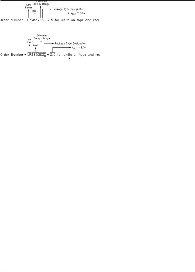
Package Type Designator is "T" for TO220 package, and "S" for TO263 package.
TABLE 1. Package Marking and Ordering Information
Output |
|
|
Description |
Package |
|
|
|
Voltage |
Order Number |
(Current, Option) |
Type |
Package Marking |
Supplied As: |
||
|
|
|
|
|
|
|
|
|
|
|
SOT223-5 |
LHXB |
1000 Units on |
||
5.0 |
LP3852EMP-5.0 |
1.5A, |
Error |
Flag |
|||
|
|
|
|
|
|
|
Tape and Reel |
|
|
|
|
|
|
|
|
|
|
|
|
|
|
||
5.0 |
LP3852EMPX-5.0 |
1.5A, |
Error |
Flag |
SOT223-5 |
LHXB |
2000 Units on |
|
|
|
|
|
|
|
Tape and Reel |
|
|
|
|
|
|
|
|
|
|
|
TO263-5 |
LP3852ES-5.0 |
Rail |
||
5.0 |
LP3852ES-5.0 |
1.5A, |
Error |
Flag |
|||
|
|
|
|
|
|
|
|
|
|
|
|
|
|
||
5.0 |
LP3852ESX-5.0 |
1.5A, |
Error |
Flag |
TO263-5 |
LP3852ES-5.0 |
Tape and Reel |
|
|
|
|
|
|
|
|
|
|
|
|
|
|
||
3.3 |
LP3852EMP-3.3 |
1.5A, |
Error |
Flag |
SOT223-5 |
LHVB |
1000 Units on |
|
|
|
|
|
|
|
Tape and Reel |
|
|
|
|
|
|
|
|
|
|
|
|
|
|
||
3.3 |
LP3852EMPX-3.3 |
1.5A, |
Error |
Flag |
SOT223-5 |
LHVB |
2000 Units on |
|
|
|
|
|
|
|
Tape and Reel |
|
|
|
|
|
|
|
|
|
|
|
TO263-5 |
LP3852ES-3.3 |
Rail |
||
3.3 |
LP3852ES-3.3 |
1.5A, |
Error |
Flag |
|||
|
|
|
|
|
|
|
|
|
|
|
|
|
|
||
3.3 |
LP3852ESX-3.3 |
1.5A, |
Error |
Flag |
TO263-5 |
LP3852ES-3.3 |
Tape and Reel |
|
|
|
|
|
|
||
2.5 |
LP3852EMP-2.5 |
1.5A, |
Error |
Flag |
SOT223-5 |
LHUB |
1000 Units on |
|
|
|
|
|
|
|
Tape and Reel |
|
|
|
|
|
|
|
|
|
|
|
|
|
|
||
2.5 |
LP3852EMPX-2.5 |
1.5A, |
Error |
Flag |
SOT223-5 |
LHUB |
2000 Units on |
|
|
|
|
|
|
|
Tape and Reel |
|
|
|
|
|
|
|
|
|
|
|
TO263-5 |
LP3852ES-2.5 |
Rail |
||
2.5 |
LP3852ES-2.5 |
1.5A, |
Error |
Flag |
|||
|
|
|
|
|
|
|
|
|
|
|
|
|
|
||
2.5 |
LP3852ESX-2.5 |
1.5A, |
Error |
Flag |
TO263-5 |
LP3852ES-2.5 |
Tape and Reel |
|
|
|
|
|
|
||
1.8 |
LP3852ES-1.8 |
1.5A, |
Error |
Flag |
TO263-5 |
LP3852ES-1.8 |
Rail |
|
|
|
|
|
|
|
|
|
|
|
|
|
|
||
1.8 |
LP3852ESX-1.8 |
1.5A, |
Error |
Flag |
TO263-5 |
LP3852ES-1.8 |
Tape and Reel |
|
|
|
|
|
|
|
|
|
|
|
|
|
|
||
1.8 |
LP3852EMP-1.8 |
1.5A, |
Error |
Flag |
SOT223-5 |
LHTB |
1000 Units on |
|
|
|
|
|
|
|
Tape and Reel |
|
|
|
|
|
|
|
|
|
|
|
SOT223-5 |
LHTB |
2000 Units on |
||
1.8 |
LP3852EMPX-1.8 |
1.5A, |
Error |
Flag |
|||
|
|
|
|
|
|
|
Tape and Reel |
|
|
|
|
|
|
|
|
5.0 |
LP3855EMP-5.0 |
1.5A, SENSE |
SOT223-5 |
LJ2B |
1000 Units on |
||
|
|
|
|
|
|
|
Tape and Reel |
|
|
|
|
|
|
|
|
5.0 |
LP3855EMPX-5.0 |
1.5A, SENSE |
SOT223-5 |
LJ2B |
2000 Units on |
||
|
|
|
|
|
|
|
Tape and Reel |
|
|
|
|
|
|
|
|
5.0 |
LP3855ES-5.0 |
1.5A, SENSE |
TO263-5 |
LP3855ES-5.0 |
Rail |
||
|
|
|
|
|
|
|
|
5.0 |
LP3855ESX-5.0 |
1.5A, SENSE |
TO263-5 |
LP3855ES-5.0 |
Tape and Reel |
||
|
|
|
|
|
|
|
|
3.3 |
LP3855EMP-3.3 |
1.5A, SENSE |
SOT223-5 |
LJ1B |
1000 Units on |
||
|
|
|
|
|
|
|
Tape and Reel |
|
|
|
|
|
|
|
|
www.national.com |
4 |

Ordering Information |
(Continued) |
|
|
|
|||
|
TABLE 1. Package Marking and Ordering Information (Continued) |
|
|||||
|
|
|
|
|
|
|
|
Output |
|
|
Description |
Package |
|
|
|
Voltage |
Order Number |
(Current, Option) |
Type |
Package Marking |
Supplied As: |
||
|
|
|
|
|
|
|
|
3.3 |
LP3855EMPX-3.3 |
1.5A, SENSE |
SOT223-5 |
LJ1B |
2000 Units on |
||
|
|
|
|
|
|
|
Tape and Ree |
|
|
|
|
|
|
|
|
3.3 |
LP3855ES-3.3 |
1.5A, SENSE |
TO263-5 |
LP3855ES-3.3 |
Rail |
||
|
|
|
|
|
|
|
|
3.3 |
LP3855ESX-3.3 |
1.5A, SENSE |
TO263-5 |
LP3855ES-3.3 |
Tape and Reel |
||
|
|
|
|
|
|
|
|
2.5 |
LP3855EMP-2.5 |
1.5A, SENSE |
SOT223-5 |
LHZB |
1000 Units on |
||
|
|
|
|
|
|
|
Tape and Reel |
|
|
|
|
|
|
|
|
2.5 |
LP3855EMPX-2.5 |
1.5A, SENSE |
SOT223-5 |
LHZB |
2000 Units on |
||
|
|
|
|
|
|
|
Tape and Ree |
|
|
|
|
|
|
|
|
2.5 |
LP3855ES-2.5 |
1.5A, SENSE |
TO263-5 |
LP3855ES-2.5 |
Rail |
||
|
|
|
|
|
|
|
|
2.5 |
LP3855ESX-2.5 |
1.5A, SENSE |
TO263-5 |
LP3855ES-2.5 |
Tape and Reel |
||
|
|
|
|
|
|
|
|
1.8 |
LP3855EMP-1.8 |
1.5A, SENSE |
SOT223-5 |
LHYB |
1000 Units on |
||
|
|
|
|
|
|
|
Tape and Reel |
|
|
|
|
|
|
|
|
1.8 |
LP3855EMPX-1.8 |
1.5A, SENSE |
SOT223-5 |
LHYB |
|
||
|
|
|
|
|
|
|
|
1.8 |
LP3855ES-1.8 |
1.5A, SENSE |
TO263-5 |
LP3855ES-1.8 |
Rail |
||
|
|
|
|
|
|
|
|
1.8 |
LP3855ESX-1.8 |
1.5A, SENSE |
TO263-5 |
LP3855ES-1.8 |
Tape and Reel |
||
|
|
|
|
|
|
|
|
|
|
|
|
|
|
||
5.0 |
LP3852ET-5.0 |
1.5A, |
Error |
Flag |
TO220-5 |
LP3852ET-5.0 |
Rail |
|
|
|
|
|
|
|
|
|
|
|
|
|
|
||
3.3 |
LP3852ET-3.3 |
1.5A, |
Error |
Flag |
TO220-5 |
LP3852ET-3.3 |
Rail |
|
|
|
|
|
|
|
|
|
|
|
|
|
|
||
2.5 |
LP3852ET-2.5 |
1.5A, |
Error |
Flag |
TO220-5 |
LP3852ET-2.5 |
Rail |
|
|
|
|
|
|
|
|
|
|
|
|
|
|
||
1.8 |
LP3852ET-1.8 |
1.5A, |
Error |
Flag |
TO220-5 |
LP3852ET-1.8 |
Rail |
|
|
|
|
|
|
|
|
5.0 |
LP3855ET-5.0 |
1.5A, SENSE |
TO220-5 |
LP3855ET-5.0 |
Rail |
||
|
|
|
|
|
|
|
|
3.3 |
LP3855ET-3.3 |
1.5A, SENSE |
TO220-5 |
LP3855ET-3.3 |
Rail |
||
|
|
|
|
|
|
|
|
2.5 |
LP3855ET-2.5 |
1.5A, SENSE |
TO220-5 |
LP3855ET-2.5 |
Rail |
||
|
|
|
|
|
|
|
|
1.8 |
LP3855ET-1.8 |
1.5A, SENSE |
TO220-5 |
LP3855ET-1.8 |
Rail |
||
|
|
|
|
|
|
|
|
LP3852/LP3855
5 |
www.national.com |

LP3852/LP3855
Block Diagrams
LP3852
20031003
LP3855
20031029
www.national.com |
6 |

Absolute Maximum Ratings (Note 1)
If Military/Aerospace specified devices are required, please contact the National Semiconductor Sales Office/ Distributors for availability and specifications.
Storage Temperature Range |
−65˚C to +150˚C |
Lead Temperature |
|
(Soldering, 5 sec.) |
260˚C |
ESD Rating (Note 3) |
2 kV |
Power Dissipation (Note 2) |
Internally Limited |
Input Supply Voltage (Survival) |
−0.3V to +7.5V |
Shutdown Input Voltage |
|
(Survival) |
−0.3V to 7.5V |
Output Voltage (Survival), (Note |
|
6), (Note 7) |
−0.3V to +6.0V |
IOUT (Survival) |
Short Circuit Protected |
||
Maximum Voltage for |
ERROR |
|
|
Pin |
VIN |
||
Maximum Voltage for SENSE Pin |
VOUT |
||
Operating Ratings
Input Supply Voltage (Note 11) |
2.5V to 7.0V |
Shutdown Input Voltage |
−0.3V to 7.0V |
Maximum Operating Current (DC) |
1.5A |
Junction Temperature |
−40˚C to +125˚C |
Electrical Characteristics
LP3852/LP3855
Limits in standard typeface are for TJ = 25˚C, and limits in boldface type apply over the full operating temperature range. Unless otherwise specified: VIN = VO(NOM) + 1V, IL = 10 mA, COUT = 10µF, VSD = 2V.
Symbol |
Parameter |
Conditions |
Typ |
LP3852/5 (Note 5) |
Units |
||
|
|
|
(Note |
|
|
|
|
|
|
|
Min |
Max |
|
||
|
|
|
4) |
|
|||
|
|
|
|
|
|
||
|
|
|
|
|
|
|
|
|
Output Voltage |
VOUT +1V ≤ VIN ≤ 7.0V |
|
-1.5 |
+1.5 |
|
|
VO |
Tolerance |
10 mA ≤ IL ≤ 1.5A |
0 |
% |
|||
-3.0 |
+3.0 |
||||||
|
(Note 8) |
|
|
|
|||
|
|
|
|
|
|
||
|
|
|
|
|
|
|
|
∆V OL |
Output Voltage Line |
VOUT +1V ≤ VIN ≤ 7.0V |
0.02 |
|
|
% |
|
|
Regulation (Note 8) |
|
0.06 |
|
|
|
|
|
|
|
|
|
|
|
|
∆VO/ ∆IOUT |
Output Voltage Load |
10 mA ≤ IL ≤ 1.5A |
0.06 |
|
|
% |
|
|
Regulation |
|
0.12 |
|
|
|
|
|
(Note 8) |
|
|
|
|
|
|
|
|
|
|
|
|
|
|
VIN - VOUT |
Dropout Voltage |
IL = 150 mA |
24 |
|
35 |
|
|
|
|
|
|
45 |
|
||
|
TO-263 and TO-220 |
|
|
|
|
||
|
|
|
|
|
|
||
|
IL = 1.5A |
240 |
|
280 |
|
||
|
(Note 10) |
|
mV |
||||
|
|
|
|
380 |
|||
|
|
|
|
|
|
||
|
|
|
|
|
|
|
|
|
Dropout Voltage |
IL = 150mA |
26 |
|
35 |
|
|
|
|
|
|
45 |
|
||
|
SOT 223 |
|
|
|
|
||
|
|
|
|
|
|
||
|
IL = 1.5A |
260 |
|
320 |
|
||
|
(Note 10), (Note 12) |
|
|
||||
|
|
|
|
435 |
|
||
|
|
|
|
|
|
||
|
|
|
|
|
|
|
|
|
|
IL = 150 mA |
3 |
|
9 |
|
|
IGND |
Ground Pin Current In |
|
|
|
10 |
mA |
|
Normal Operation Mode |
|
|
|
|
|||
IL = 1.5A |
3 |
|
9 |
||||
|
|
|
|
|
10 |
|
|
|
|
|
|
|
|
|
|
IGND |
Ground Pin Current In |
VSD ≤ 0.3V |
0.01 |
|
10 |
µA |
|
|
Shutdown Mode |
-40˚C ≤ TJ ≤ 85˚C |
|
|
50 |
|
|
IO(PK) |
Peak Output Current |
VO ≥ VO(NOM) - 4% |
1.8 |
|
|
A |
|
Short Circuit Protection |
|
|
|
|
|
||
|
|
|
|
|
|
|
|
ISC |
Short Circuit Current |
|
3.2 |
|
|
A |
|
LP3852/LP3855
7 |
www.national.com |

LP3852/LP3855
Electrical Characteristics
LP3852/LP3855 (Continued)
Limits in standard typeface are for TJ = 25˚C, and limits in boldface type apply over the full operating temperature range. Unless otherwise specified: VIN = VO(NOM) + 1V, IL = 10 mA, COUT = 10µF, VSD = 2V.
|
Symbol |
|
|
|
Parameter |
Conditions |
Typ |
LP3852/5 (Note 5) |
Units |
||
|
|
|
|
|
|
|
|
(Note |
|
|
|
|
|
|
|
|
|
|
|
Min |
Max |
|
|
|
|
|
|
|
|
|
|
4) |
|
||
|
|
|
|
|
|
|
|
|
|
|
|
|
|
|
|
|
|
|
|
|
|
|
|
|
Shutdown Input |
|
|
|
|
|
|||||
|
|
|
|
|
|
|
|
|
|
|
|
|
VSDT |
|
Shutdown Threshold |
Output = High |
VIN |
2 |
|
V |
|||
|
|
Output = Low |
0 |
|
0.3 |
||||||
|
|
|
|
|
|
|
|
|
|||
|
|
|
|
|
|
|
|
|
|
|
|
|
TdOFF |
|
Turn-off delay |
IL = 1.5A |
20 |
|
|
µs |
|||
|
TdON |
|
Turn-on delay |
IL = 1.5A |
25 |
|
|
µs |
|||
|
ISD |
|
|
|
VSD = VIN |
1 |
|
|
nA |
||
|
|
SD |
Input Current |
|
|
||||||
|
|
Flag |
|
|
|
|
|
|
|
|
|
|
Error |
|
|
|
|
|
|
|
|
||
|
VT |
|
Threshold |
(Note 9) |
10 |
5 |
16 |
% |
|||
|
VTH |
|
Threshold Hysteresis |
(Note 9) |
5 |
2 |
8 |
% |
|||
|
VEF(Sat) |
|
|
Isink = 100µA |
0.02 |
|
0.1 |
V |
|||
|
|
Error |
Flag Saturation |
|
|||||||
|
Td |
|
Flag Reset Delay |
|
1 |
|
|
µs |
|||
|
|
|
|
|
|
|
|
|
|
|
|
|
Ilk |
|
|
|
1 |
|
|
nA |
|||
|
|
Error |
Flag Pin Leakage |
|
|
|
|||||
|
|
|
|
Current |
|
|
|
|
|
||
|
|
|
|
|
|
|
|
|
|
|
|
|
Imax |
|
|
VError = 0.5V |
1 |
|
|
mA |
|||
|
|
Error |
Flag Pin Sink |
|
|
||||||
|
|
|
|
Current |
|
|
|
|
|
||
|
|
|
|
|
|
|
|
|
|
|
|
|
AC Parameters |
|
|
|
|
|
|
|
|
||
|
|
|
|
|
|
|
|
|
|
|
|
|
|
|
|
|
|
|
VIN = VOUT + 1V |
73 |
|
|
|
|
|
|
|
|
|
|
COUT = 10uF |
|
|
|
|
|
PSRR |
|
Ripple Rejection |
VOUT = 3.3V, f = 120Hz |
|
|
|
dB |
|||
|
|
VIN = VOUT + 0.5V |
57 |
|
|
||||||
|
|
|
|
|
|
|
|
|
|
||
|
|
|
|
|
|
|
COUT = 10uF |
|
|
|
|
|
|
|
|
|
|
|
VOUT = 3.3V, f = 120Hz |
|
|
|
|
|
ρn(l/f) |
|
Output Noise Density |
f = 120Hz |
0.8 |
|
|
µV |
|||
|
|
|
|
|
|
|
BW = 10Hz – 100kHz |
150 |
|
|
|
|
en |
|
Output Noise Voltage |
VOUT = 2.5V |
|
|
|
µV (rms) |
|||
|
|
BW = 300Hz – 300kHz |
100 |
|
|
||||||
|
|
|
|
|
|
|
|
|
|
||
|
|
|
|
|
|
|
VOUT = 2.5V |
|
|
|
|
Note 1: Absolute maximum ratings indicate limits beyond which damage to the device may occur. Operating ratings indicate conditions for which the device is intended to be functional, but does not guarantee specific performance limits. For guaranteed specifications and test conditions, see Electrical Characteristics. The guaranteed specifications apply only for the test conditions listed. Some performance characteristics may degrade when the device is not operated under the listed test conditions.
Note 2: At elevated temperatures, devices must be derated based on package thermal resistance. The devices in TO220 package must be derated at θjA = 50˚C/W (with 0.5in2, 1oz. copper area), junction-to-ambient (with no heat sink). The devices in the TO263 surface-mount package must be derated at θjA = 60˚C/W (with 0.5in2, 1oz. copper area), junction-to-ambient. See Application Hints.
Note 3: The human body model is a 100pF capacitor discharged through a 1.5kΩ resistor into each pin.
Note 4: Typical numbers are at 25˚C and represent the most likely parametric norm.
Note 5: Limits are guaranteed by testing, design, or statistical correlation.
Note 6: If used in a dual-supply system where the regulator load is returned to a negative supply, the output must be diode-clamped to ground.
Note 7: The output PMOS structure contains a diode between the VIN and VOUT terminals. This diode is normally reverse biased. This diode will get forward biased if the voltage at the output terminal is forced to be higher than the voltage at the input terminal. This diode can typically withstand 200mA of DC current and 1Amp of peak current.
Note 8: Output voltage line regulation is defined as the change in output voltage from the nominal value due to change in the input line voltage. Output voltage load regulation is defined as the change in output voltage from the nominal value due to change in load current. The line and load regulation specification contains only the typical number. However, the limits for line and load regulation are included in the output voltage tolerance specification.
Note 9: Error Flag threshold and hysteresis are specified as percentage of regulated output voltage. See Application Hints.
Note 10: Dropout voltage is defined as the minimum input to output differential voltage at which the output drops 2% below the nominal value. Dropout voltage specification applies only to output voltages of 2.5V and above. For output voltages below 2.5V, the drop-out voltage is nothing but the input to output differential, since the minimum input voltage is 2.5V.
Note 11: The minimum operating value for VIN is equal to either [VOUT(NOM) + VDROPOUT] or 2.5V, whichever is greater.
Note 12: The SOT 223 package devices have slightly higher dropout due to increased bond wire resistance.
www.national.com |
8 |

Typical Performance Characteristics Unless otherwise specified: TJ = 25˚C, COUT = 10µF, CIN = 10µF, S/D pin is tied to VIN, VOUT = 2.5V, VIN = VO(NOM) + 1V, IL = 10 mA.
|
Ground Current vs Output Voltage |
Dropout Voltage vs Output Load Current |
IL = 1.5A |
20031062
|
20031054 |
Shutdown IQ vs Junction Temperature |
Errorflag Threshold vs Junction Temperature |
20031055 |
20031057 |
DC Load Reg. vs Junction Temperature |
DC Line Regulation vs Temperature |
20031058 |
20031059 |
LP3852/LP3855
9 |
www.national.com |

LP3852/LP3855
Typical Performance Characteristics Unless otherwise specified: TJ = 25˚C, COUT = 10µF, CIN = 10µF, S/D pin is tied to VIN, VOUT = 2.5V, VIN = VO(NOM) + 1V, IL = 10 mA. (Continued)
VIN vs VOUT Over Temperature |
Noise vs Frequency |
20031060 |
20031061 |
Load Transient Response |
Load Transient Response |
CIN = COUT = 10µF, OSCON |
CIN = COUT = 100µF, OSCON |
20031081 |
20031082 |
Load Transient Response |
Load Transient Response |
CIN = COUT = 100µF, POSCAP |
CIN = COUT = 10µF, TANTALUM |
20031083 |
20031084 |
www.national.com |
10 |