

Розрахункова СЗіВІ / Розрахункова робота / Стабілізатори напруги / LDO National Semiconductor / LP3883
.pdfFebruary 2006
LP3883
3A Fast-Response Ultra Low Dropout Linear Regulators
General Description
The LP3883 is a high-current, fast-response regulator which can maintain output voltage regulation with minimum input to output voltage drop. Fabricated on a CMOS process, the device operates from two input voltages: Vbias provides voltage to drive the gate of the N-MOS power transistor, while Vin is the input voltage which supplies power to the load. The use of an external bias rail allows the part to operate from ultra low Vin voltages. Unlike bipolar regulators, the CMOS architecture consumes extremely low quiescent current at any output load current. The use of an N-MOS power transistor results in wide bandwidth, yet minimum external capacitance is required to maintain loop stability.
The fast transient response of these devices makes them suitable for use in powering DSP, Microcontroller Core voltages and Switch Mode Power Supply post regulators. The parts are available in TO-220 and TO-263 packages.
Dropout Voltage: 210 mV (typ) @ 3A load current.
Ground Pin Current: 3 mA (typ) at full load.
Shutdown Current: 60 nA (typ) when S/D pin is low.
Precision Output Voltage: 1.5% room temperature accuracy.
Features
n Ultra low dropout voltage (210 mV @ 3A typ) n Low ground pin current
n Load regulation of 0.04%/A
n 60 nA typical quiescent current in shutdown n 1.5% output accuracy (25ûC)
n TO-220, TO-263 packages
n Over temperature/over current protection
n −40ûC to +125ûC junction temperature range
Applications
n DSP Power Supplies
n Server Core and I/O Supplies
n Linear Power Supplies for PC Add-in-Cards n Set-Top Box Power Supplies
n Microprocessor Power Supplies
n High Efficiency Linear Power Supplies n SMPS Post-Regulators
Typical Application Circuit
20062401
At least 4.7 µF of input and output capacitance is required for stability.
Regulators Linear Dropout Low Ultra Response-Fast 3A LP3883
© 2006 National Semiconductor Corporation |
DS200624 |
www.national.com |
LP3883
Connection Diagrams
20062402 |
20062403 |
TO-220, Top View |
TO-263, Top View |
Ordering Information
Order Number |
Package Type |
Package Drawing |
Supplied As |
|
|
|
|
LP3883ES-1.2 |
TO263-5 |
TS5B |
Rail |
|
|
|
|
LP3883ESX-1.2 |
TO263-5 |
TS5B |
Tape and Reel |
|
|
|
|
LP3883ET-1.2 |
TO220-5 |
T05D |
Rail |
|
|
|
|
LP3883ES-1.5 |
TO263-5 |
TS5B |
Rail |
|
|
|
|
LP3883ESX-1.5 |
TO263-5 |
TS5B |
Tape and Reel |
|
|
|
|
LP3883ET-1.5 |
TO220-5 |
T05D |
Rail |
|
|
|
|
LP3883ES-1.8 |
TO263-5 |
TS5B |
Rail |
|
|
|
|
LP3883ESX-1.8 |
TO263-5 |
TS5B |
Tape and Reel |
|
|
|
|
LP3883ET-1.8 |
TO220-5 |
T05D |
Rail |
|
|
|
|
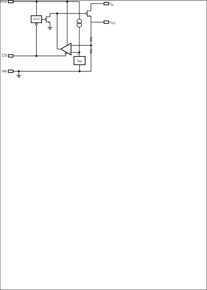
Block Diagram
20062424
www.national.com |
2 |

Absolute Maximum Ratings (Note 1)
If Military/Aerospace specified devices are required, please contact the National Semiconductor Sales Office/ Distributors for availability and specifications.
Storage Temperature Range |
−65ûC to +150ûC |
Lead Temp. (Soldering, 5 seconds) |
260ûC |
ESD Rating |
|
Human Body Model (Note 3) |
2 kV |
Machine Model (Note 10) |
200V |
Power Dissipation (Note 2) |
Internally Limited |
VIN Supply Voltage (Survival) |
−0.3V to +6V |
VBIAS Supply Voltage (Survival) |
−0.3V to +7V |
Shutdown Input Voltage (Survival) |
−0.3V to +7V |
IOUT (Survival) |
Internally Limited |
Output Voltage (Survival) |
−0.3V to +6V |
Junction Temperature |
−40ûC to +150ûC |
Operating Ratings
VIN Supply Voltage |
(VOUT + VDO) to 5.5V |
Shutdown Input Voltage |
0 to +6V |
IOUT |
3A |
Operating Junction |
−40ûC to +125ûC |
Temperature Range |
|
VBIAS Supply Voltage |
4.5V to 6V |
Electrical Characteristics Limits in standard typeface are for TJ = 25ûC, and limits in boldface type apply over the full operating temperature range. Unless otherwise specified: VIN = VO(NOM) + 1V, VBIAS = 4.5V, IL = 10 mA, CIN = COUT = 4.7 µF, VS/D = VBIAS.
|
Symbol |
|
|
Parameter |
|
|
|
|
Conditions |
Typical |
MIN |
MAX |
Units |
|
|
|
|
|
|
|
|
(Note 4) |
(Note 5) |
(Note 5) |
|||||
|
|
|
|
|
|
|
|
|
|
|
|
|||
|
|
|
|
|
|
|
|
|
|
|
|
|
|
|
VO |
|
Output Voltage Tolerance |
10 mA < IL < 3A |
|
1.198 |
1.234 |
|
|||||||
|
|
|
|
|
|
VO(NOM) + 1V ≤ VIN ≤ 5.5V |
1.216 |
|
|
|
||||
|
|
|
|
|
|
4.5V ≤ VBIAS ≤ 6V |
|
1.186 |
1.246 |
|
||||
|
|
|
|
|
|
|
|
|
|
|
|
1.478 |
1.522 |
|
|
|
|
|
|
|
|
|
|
|
|
1.5 |
|
|
V |
|
|
|
|
|
|
|
|
|
|
|
|
1.455 |
1.545 |
|
|
|
|
|
|
|
|
|
|
|
|
|
|
|
|
|
|
|
|
|
|
|
|
|
|
|
|
1.773 |
1.827 |
|
|
|
|
|
|
|
|
|
|
|
|
1.8 |
|
|
|
|
|
|
|
|
|
|
|
|
|
|
|
1.746 |
1.854 |
|
|
|
|
|
|
|
|
|
|
|
|
|
|
|
|
∆VO/∆VIN |
|
Output Voltage Line Regulation |
VO(NOM) + 1V ≤ VIN ≤ 5.5V |
0.01 |
|
|
%/V |
|||||||
|
|
|
|
(Note 7) |
|
|
|
|
|
|
|
|||
|
|
|
|
|
|
|
|
|
|
|
|
|
||
|
|
|
|
|
|
|
|
|
|
|
|
|
|
|
∆VO/∆IL |
|
Output Voltage Load Regulation |
10 mA < IL < 3A |
0.04 |
|
|
%/A |
|||||||
|
|
|
|
(Note 8) |
|
|
|
|
|
0.06 |
|
|
||
|
|
|
|
|
|
|
|
|
|
|
|
|||
|
|
|
|
|
|
|
|
|
|
|
|
|
|
|
VDO |
|
Dropout Voltage (Note 9) |
IL = 3A |
210 |
|
270 |
mV |
|||||||
|
|
|
|
|
|
|
|
|
|
|
|
420 |
||
|
|
|
|
|
|
|
|
|
|
|
|
|
|
|
|
|
|
|
|
|
|
|
|
|
|
|
|
|
|
IQ(VIN) |
|
Quiescent Current Drawn from |
10 mA < IL < 3A |
3 |
|
7 |
mA |
|||||||
|
|
|
|
VIN Supply |
|
|
|
|
|
|
8 |
|||
|
|
|
|
|
|
|
|
|
|
|
|
|||
|
|
|
|
|
|
V |
|
|
≤ 0.3V |
|
|
1 |
|
|
|
|
|
|
|
|
S/D |
0.03 |
|
µA |
|||||
|
|
|
|
|
|
|
|
|
|
|
|
30 |
||
|
|
|
|
|
|
|
|
|
|
|
|
|
|
|
|
|
|
|
|
|
|
|
|
|
|
|
|
|
|
IQ(VBIAS) |
|
Quiescent Current Drawn from |
10 mA < IL < 3A |
1 |
|
2 |
mA |
|||||||
|
|
|
|
VBIAS Supply |
|
|
|
|
|
|
3 |
|||
|
|
|
|
|
|
|
|
|
|
|
|
|||
|
|
|
|
|
|
V |
|
|
≤ 0.3V |
|
|
1 |
|
|
|
|
|
|
|
|
S/D |
0.03 |
|
µA |
|||||
|
|
|
|
|
|
|
|
|
|
|
|
30 |
||
|
|
|
|
|
|
|
|
|
|
|
|
|
|
|
|
|
|
|
|
|
|
|
|
|
|
|
|
|
|
ISC |
|
Short-Circuit Current |
VOUT = 0V |
6 |
|
|
A |
|||||||
Shutdown Input |
|
|
|
|
|
|
|
|
|
|||||
|
|
|
|
|
|
|
|
|
|
|
|
|
|
|
VSDT |
|
Output Turn-off Threshold |
Output = ON |
0.7 |
1.3 |
|
V |
|||||||
|
|
|
|
|
|
Output = OFF |
0.7 |
|
0.3 |
|||||
|
|
|
|
|
|
|
|
|||||||
|
|
|
|
|
|
|
|
|
|
|
|
|
|
|
Td (OFF) |
|
Turn-OFF Delay |
RLOAD X COUT << Td (OFF) |
20 |
|
|
µs |
|||||||
Td (ON) |
|
Turn-ON Delay |
RLOAD X COUT << Td (ON) |
15 |
|
|
||||||||
|
|
|
|
|||||||||||
I |
|
|
|
|
V |
|
=1.3V |
1 |
|
|
|
|||
|
|
|
S/D |
Input Current |
|
|
|
|
||||||
S/D |
S/D |
|
|
µA |
||||||||||
|
|
|
|
|
|
V |
|
|
≤ 0.3V |
−1 |
|
|
||
|
|
|
|
|
|
S/D |
|
|
|
|||||
LP3883
3 |
www.national.com |

LP3883
Electrical Characteristics Limits in standard typeface are for TJ = 25ûC, and limits in boldface type apply over the full operating temperature range. Unless otherwise specified: VIN = VO(NOM) + 1V, VBIAS = 4.5V, IL = 10 mA, CIN = COUT = 4.7 µF, VS/D = VBIAS. (Continued)
Symbol |
Parameter |
Conditions |
Typical |
MIN |
MAX |
Units |
|
(Note 4) |
(Note 5) |
(Note 5) |
|||||
|
|
|
|
||||
|
|
|
|
|
|
|
|
AC Parameters |
|
|
|
|
|
||
|
|
|
|
|
|
|
|
PSRR (VIN) |
Ripple Rejection for VIN Input |
VIN = VOUT +1V, f = 120 Hz |
80 |
|
|
|
|
|
Voltage |
|
|
|
|
||
|
|
|
|
|
|
||
|
|
|
|
|
|
|
|
|
|
VIN = VOUT + 1V, f = 1 kHz |
65 |
|
|
dB |
|
PSRR |
Ripple Rejection for VBIAS |
VBIAS = VOUT + 3V, f = 120 Hz |
70 |
|
|
||
|
|
|
|||||
(VBIAS) |
Voltage |
|
|
|
|
||
|
|
|
|
|
|||
|
|
VBIAS = VOUT + 3V, f = 1 kHz |
65 |
|
|
|
|
|
Output Noise Density |
f = 120 Hz |
1 |
|
|
µV/root−Hz |
|
|
|
|
|
|
|
|
|
en |
Output Noise Voltage |
BW = 10 Hz − 100 kHz |
150 |
|
|
µV (rms) |
|
|
VOUT = 1.8V |
BW = 300 Hz − 300 kHz |
90 |
|
|
||
|
|
|
|
||||
|
|
|
|
|
|
|
|
Note 1: Absolute maximum ratings indicate limits beyond which damage to the component may occur. Operating ratings indicate conditions for which the device is intended to be functional, but do not guarantee specific performance limits. For guaranteed specifications, see Electrical Characteristics. Specifications do not apply when operating the device outside of its rated operating conditions.
Note 2: At elevated temperatures, device power dissipation must be derated based on package thermal resistance and heatsink thermal values. θJ-A for TO-220 devices is 65ûC/W if no heatsink is used. If the TO-220 device is attached to a heatsink, a θJ-S value of 4ûC/W can be assumed. θJ-A for TO-263 devices is approximately 40ûC/W if soldered down to a copper plane which is at least 1.5 square inches in area. If power dissipation causes the junction temperature to exceed specified limits, the device will go into thermal shutdown.
Note 3: The human body model is a 100 pF capacitor discharged through a 1.5k resistor into each pin.
Note 4: Typical numbers represent the most likely parametric norm for 25ûC operation.
Note 5: Limits are guaranteed through testing, statistical correlation, or design.
Note 6: If used in a dual-supply system where the regulator load is returned to a negative supply, the output pin must be diode clamped to ground.
Note 7: Output voltage line regulation is defined as the change in output voltage from nominal value resulting from a change in input voltage.
Note 8: Output voltage load regulation is defined as the change in output voltage from nominal value as the load current increases from no load to full load.
Note 9: Dropout voltage is defined as the minimum input to output differential required to maintain the output with 2% of nominal value.
Note 10: The machine model is a 220 pF capacitor discharged directly into each pin. The machine model ESD rating of pin 5 is 100V.
www.national.com |
4 |
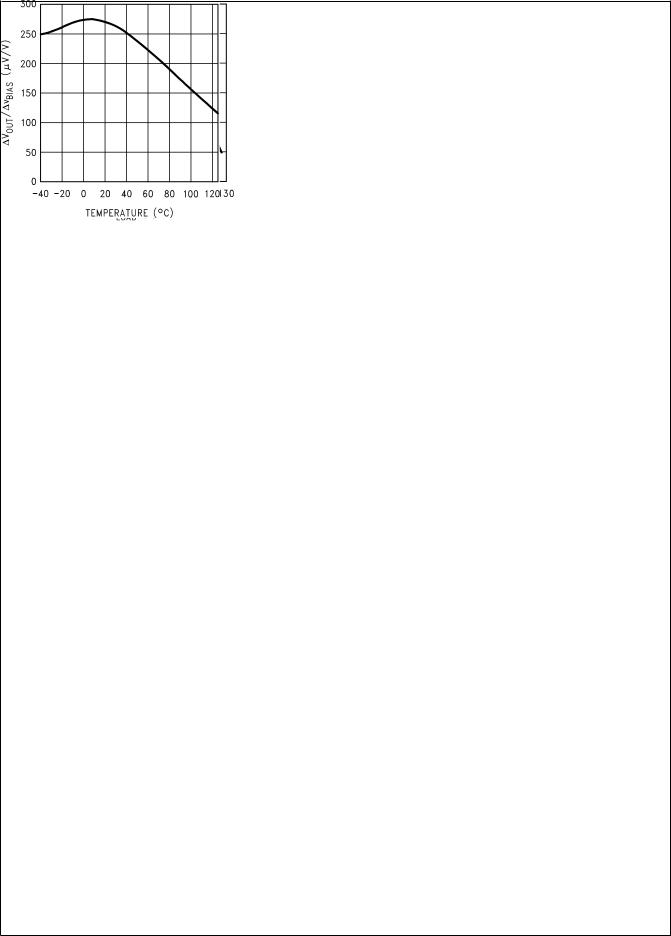
Typical Performance Characteristics
Unless otherwise specified: TA = 25ûC, COUT = 4.7µF, Cin
= 4.7µF, S/D pin is tied to VBIAS, VIN = 2.2V, VOUT = 1.8V.
Dropout vs IL |
IGND vs VSD |
|
20062404 |
20062405 |
|
|
|
VOUT vs Temperature |
|
DC Load Regulation |
20062406 |
20062407 |
Line Regulation vs VIN |
Line Regulation vs VBIAS |
20062408 |
20062409 |
LP3883
5 |
www.national.com |
LP3883
Typical Performance Characteristics Unless otherwise specified: TA = 25ûC, COUT = 4.7µF, Cin =
4.7µF, S/D pin is tied to VBIAS, VIN = 2.2V, VOUT = 1.8V. (Continued)
IBIAS vs IL |
IBIAS vs VBIAS |
20062410 |
20062411 |
IGND vs VSD |
Noise Measurement |
|
20062412 |
20062414 |
VOUTStartup Waveform |
|
VOUTStartup Waveform |
20062415 |
20062416 |
www.national.com |
6 |
Typical Performance Characteristics Unless otherwise specified: TA = 25ûC, COUT = 4.7µF, Cin =
4.7µF, S/D pin is tied to VBIAS, VIN = 2.2V, VOUT = 1.8V. (Continued)
VOUTStartup Waveform |
Line Regulation vs VBIAS |
20062418
|
20062417 |
Line Regulation vs VBIAS |
VIN PSRR |
|
20062419 |
|
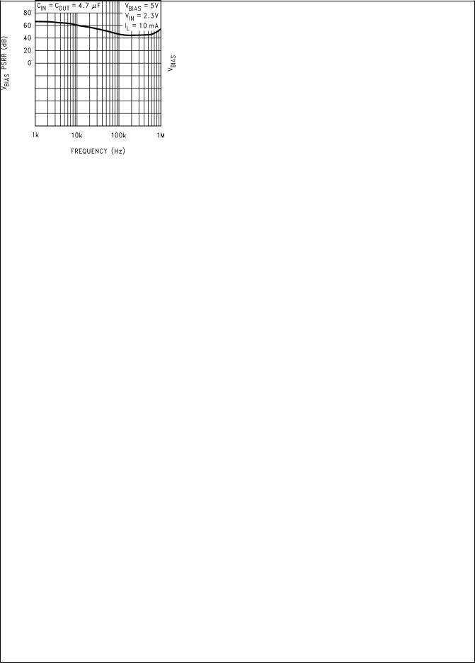
20062420 |
VIN PSRR |
VBIAS PSRR |
20062423 |
20062422 |
LP3883
7 |
www.national.com |
LP3883
Typical Performance Characteristics Unless otherwise specified: TA = 25ûC, COUT = 4.7µF, Cin =
4.7µF, S/D pin is tied to VBIAS, VIN = 2.2V, VOUT = 1.8V. (Continued)
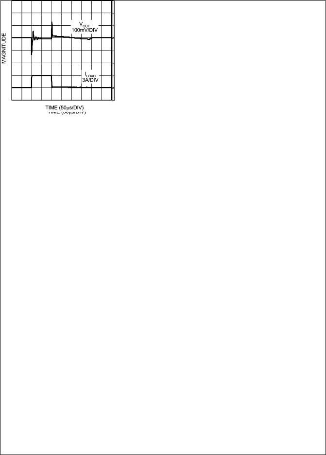
Load Transient Response |
Load Transient Response |
(Both Oscon 10µF/3A) |
(Both Oscon 100µF/3A) |
|
20062440 |
20062441 |
Load Transient Response |
|
Load Transient Response |
(Both POSCAP 100µF/3A) |
|
(SANYO 150µF/3A) |
|
20062442 |
|
20062443 |
Load Transient Response |
Load Transient Response |
(Tantalum 10µF/3A) |
(Tantalum 100µF/3A) |
20062444 |
20062445 |
www.national.com |
8 |
Typical Performance Characteristics Unless otherwise specified: TA = 25ûC, COUT = 4.7µF, Cin =
4.7µF, S/D pin is tied to VBIAS, VIN = 2.2V, VOUT = 1.8V. (Continued)
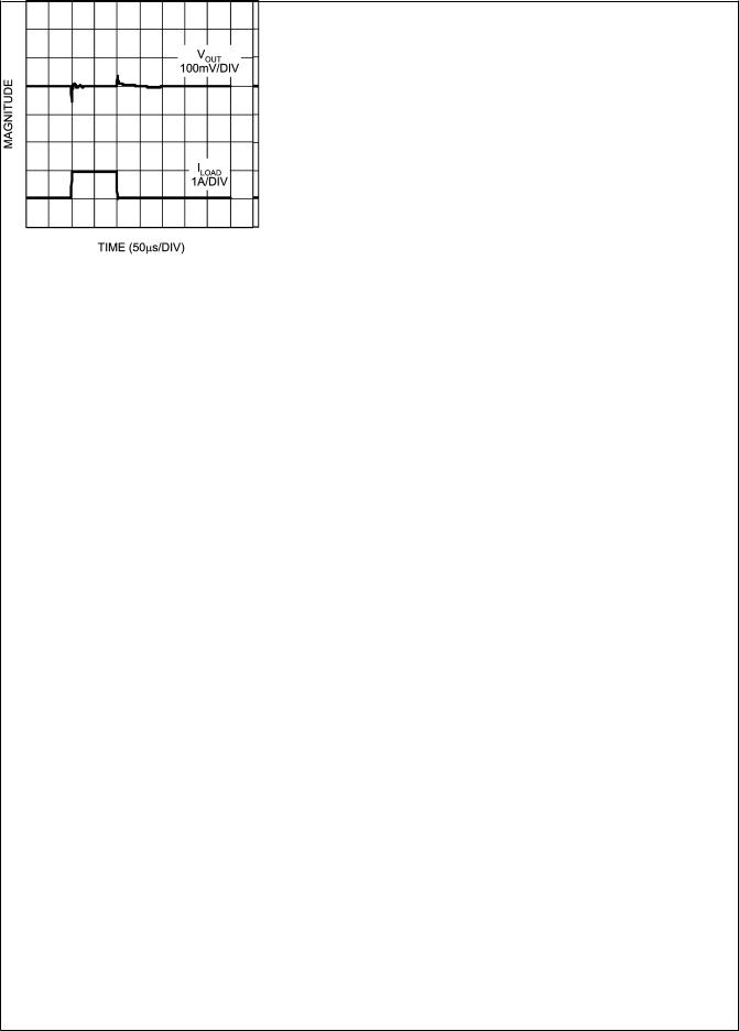
Load Transient Response |
Load Transient Response |
(Both Oscon 10µF/1A) |
(Both Oscon 100µF/1A) |
20062446 |
20062447 |
Load Transient Response |
Load Transient Response |
(Both POSCAP 100µF/1A) |
(SANYO 150µF/1A) |
|
20062448 |
20062451 |
|
|
|
Load Transient Response |
|
Load Transient Response |
(Tantalum 10µF/1A) |
|
(Tantalum 100µF/1A) |
20062449 |
20062450 |
LP3883
9 |
www.national.com |
LP3883
Application Hints
EXTERNAL CAPACITORS
To assure regulator stability, input and output capacitors are required as shown in the Typical Application Circuit.
OUTPUT CAPACITOR
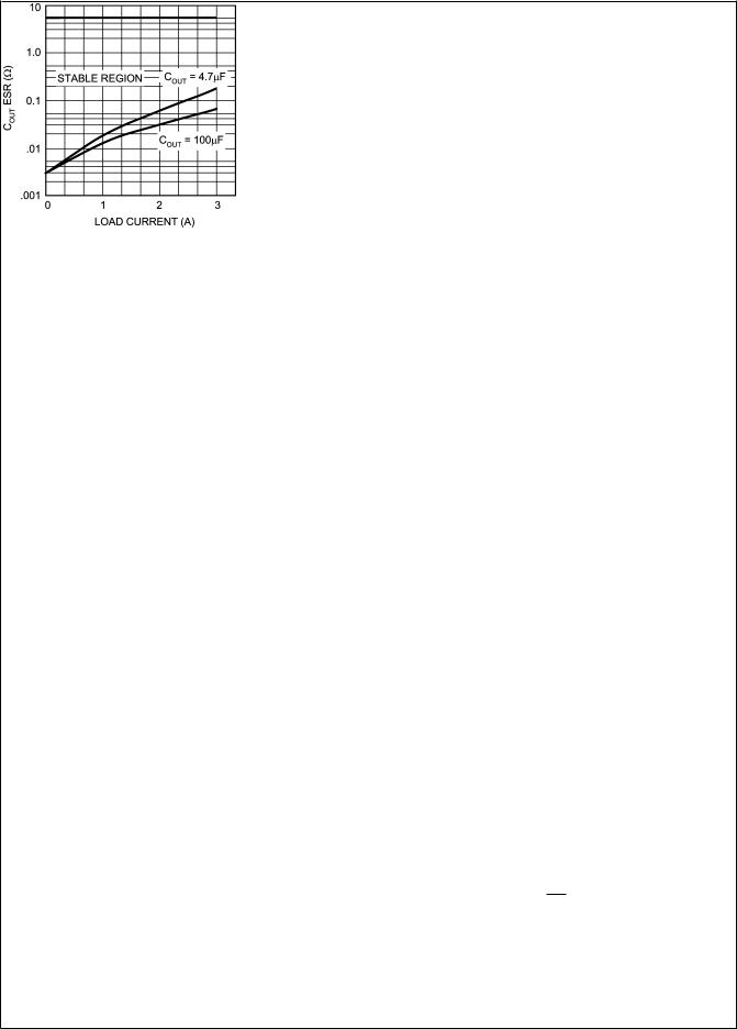
At least 4.7µF of output capacitance is required for stability (the amount of capacitance can be increased without limit). The output capacitor must be located less than 1 cm from the output pin of the IC and returned to a clean analog ground. The ESR (equivalent series resistance) of the output capacitor must be within the "stable" range as shown in the graph below over the full operating temperature range for stable operation.
20062431
Minimum ESR vs Output Load Current
Tantalum capacitors are recommended for the output as their ESR is ideally suited to the partÕs requirements and the ESR is very stable over temperature. Aluminum electrolytics are not recommended because their ESR increases very rapidly at temperatures below 10C. Aluminum caps can only be used in applications where lower temperature operation is not required.
A second problem with Al caps is that many have ESRÕs which are only specified at low frequencies. The typical loop bandwidth of a linear regulator is a few hundred kHz to several MHz. If an Al cap is used for the output cap, it must be one whose ESR is specified at a frequency of 100 kHz or more.
Because the ESR of ceramic capacitors is only a few milli Ohms, they are not suitable for use as output capacitors on LP388X devices. The regulator output can tolerate ceramic capacitance totaling up to 15% of the amount of Tantalum capacitance connected from the output to ground.
OUTPUT "BYPASS" CAPACITORS
Many designers place small value "bypass" capacitors at various circuit points to reduce noise. Ceramic capacitors in the value range of about 1000pF to 0.1µF placed directly on the output of a PNP or P-FET LDO regulator can cause a loss of phase margin which can result in oscillations, even when a Tantalum output capacitor is in parallel with it. This is not unique to National Semiconductor LDO regulators, it is true of any P-type LDO regulator.
The reason for this is that PNP or P-FET regulators have a higher output impedance (compared to an NPN regulator), which results in a pole-zero pair being formed by every different capacitor connected to the output.
The zero frequency is approximately:
Fz = 1 / (2 X π X ESR X C)
Where ESR is the equivalent series resistance of the capacitor, and C is the value of capacitance.
The pole frequency is:
Fp = 1 / (2 X π X RL X C)
Where RL is the load resistance connected to the regulator output.
To understand why a small capacitor can reduce phase margin: assume a typical LDO with a bandwidth of 1MHz, which is delivering 0.5A of current from a 2.5V output (which means RL is 5 Ohms). We then place a .047 µF capacitor on the output. This creates a pole whose frequency is:
Fp = 1 / (2 X π X 5 X .047 X 10E-6) = 677 kHz
This pole would add close to 60 degrees of phase lag at the crossover (unity gain) frequency of 1 MHz, which would almost certainly make this regulator oscillate. Depending on the load current, output voltage, and bandwidth, there are usually values of small capacitors which can seriously reduce phase margin. If the capacitors are ceramic, they tend to oscillate more easily because they have very little internal inductance to damp it out. If bypass capacitors are used, it is best to place them near the load and use trace inductance to "decouple" them from the regulator output.
INPUT CAPACITOR
The input capacitor must be at least 4.7 µF, but can be increased without limit. ItÕs purpose is to provide a low source impedance for the regulator input. Ceramic capacitors work best for this, but Tantalums are also very good. There is no ESR limitation on the input capacitor (the lower, the better). Aluminum electrolytics can be used, but their ESR increase very quickly at cold temperatures. They are not recommended for any application where temperatures go below about 10ûC.
BIAS CAPACITOR
The 0.1µF capacitor on the bias line can be any good quality capacitor (ceramic is recommended).
BIAS VOLTAGE
The bias voltage is an external voltage rail required to get gate drive for the N-FET pass transistor. Bias voltage must be in the range of 4.5 - 6V to assure proper operation of the part.
UNDER VOLTAGE LOCKOUT
The bias voltage is monitored by a circuit which prevents the regulator output from turning on if the bias voltage is below approximately 4V.
SHUTDOWN OPERATION
Pulling down the shutdown (S/D) pin will turn-off the regulator. Pin S/D must be actively terminated through a pull-up resistor (10 kΩ to 100 kΩ) for a proper operation. If this pin is driven from a source that actively pulls high and low (such as a CMOS rail to rail comparator), the pull-up resistor is not required. This pin must be tied to Vin if not used.
www.national.com |
10 |