

Розрахункова СЗіВІ / Розрахункова робота / Стабілізатори напруги / LDO National Semiconductor / LP3987
.pdfFebruary 2007
LP3987
Micropower micro SMD 150 mA Ultra Low-Dropout CMOS Voltage Regulators with Sleep MODE
General Description
The LP3987 is a 150mA fixed output voltage regulator with very low dropout voltage designed specially to meet requirements of battery-powered applications. The additional sleep MODE feature will reduce current consumption during standby operation to prolong the usage of battery.
Dropout Voltage: 100mV maximum dropout with 150mA load.
Shutdown: Less than 1µA quiescent current.
Sleep Mode: Typically 14µA quiescent current during sleep MODE to reduce battery consumption.
Enhanced Stability: The LP3987 is stable with minimum 1µF ±20% low ESR ceramic output capacitor as low as 5mΩ and high quality tantalum capacitors.
The LP3987 is available in a thin 5 Bump micro SMD package. Performance is specified for −40°C to 125°C.
This device is available with output voltage options of 2.5V, 2.6V, 2.8V, 2.85V & 3.0V. For other voltage options, please contact National Semiconductor Corporation.
Features
■Miniature 5-I/O micro SMD package
■Stable with ceramic and high quality tantalum output capacitors
■Logic controlled enable
■Thermal Shutdown and short-circuit current limit
Key Specifications
■2.7 to 6.0V input range
■Guaranteed 150 mA output current
■1µA quiescent current on shutdown
■100 mV maximum dropout with 150 mA load
■50dB PSRR at 10KHz
■Sleep MODE features
■Over temperature & over current protection
■−40°C to +125°C junction temperature range for operation
Applications
■CDMA cellular handsets
■Wideband CDMA cellular handsets
■GSM cellular handsets
■Portable information appliances
■µP/DSP Power Supplies
■Digital Cameras
■SRAM Backup
Typical Application Circuit
20022201
sleep with Regulators Voltage CMOS Dropout-Low Ultra mA 150 SMD micro Micropower LP3987
MODE
© 2007 National Semiconductor Corporation |
200222 |
www.national.com |

LP3987
Block Diagram
LP3987
20022202
Connection Diagram
20022271
Top View
5 I/O micro SMD Package See NS Package Number TLA05
www.national.com |
2 |

Pin Descriptions
Name |
micro SMD* |
Function |
VEN |
A1 |
Enable Input Logic, Enable High |
GND |
B2 |
Common Ground |
|
|
|
VOUT |
C1 |
Output voltage of the LDO |
VIN |
C3 |
Input voltage of the LDO |
MODE |
A3 |
Power Mode Control, Active = 1, Sleep Mode |
|
|
= 0 |
|
|
|
* The pin numbering scheme for the micro SMD package was revised in April, 2002 to conform to JEDEC standard. Only the pin numbers were revised. No changes to the physical location of the inputs/outputs were made. For reference purposes, the obsolete numbering scheme had VEN as pin 1, GND as pin 2, VOUT as pin 3, VIN as pin 4, and MODE as pin 5.
Ordering Information
Output Voltage (V) |
Grade |
LP3987 Supplied as 250 Units, Tape and |
LP3987 Supplied as 3000 Units, Tape |
|
Reel |
and Reel |
|||
|
|
|||
2.5 |
STD |
LP3987ITL-2.5 |
LP3987ITLX-2.5 |
|
2.6 |
STD |
LP3987ITL-2.6 |
LP3987ITLX-2.6 |
|
|
|
|
|
|
2.8 |
STD |
LP3987ITL-2.8 |
LP3987ITLX-2.8 |
|
|
|
|
|
|
2.85 |
STD |
LP3987ITL-2.85 |
LP3987ITLX-2.85 |
|
3.0 |
STD |
LP3987ITL-3.0 |
LP3987ITLX-3.0 |
|
|
|
|
|
LP3987
3 |
www.national.com |

LP3987
Absolute Maximum Ratings (Notes 1, 2)
If Military/Aerospace specified devices are required, please contact the National Semiconductor Sales Office/ Distributors for availability and specifications.
VIN |
−0.3 to 6.5V |
VEN, VMODE |
−0.3 to 6.5V |
VOUT |
−0.3V to(V IN+ 0.3V) |
|
≤ 6.5 |
Storage Temperature |
−65°C to +150°C |
ESD (Note 4) |
|
Human Body Model |
2KV |
Machine Model |
200V |
Maximum Power Dissipation (Note 3) |
|
θJA (micro SMD small bump) |
255°C/W |
Operating Ratings (Notes 1, 2)
VIN |
VOUT+ 200mV to 6V |
VEN, VMODE |
0 to 6.0V |
Junction Temperature |
−40°C to +125°C |
Maximum Power Dissipation (Note 3) |
392mW at 25°C |
Electrical Characteristics
Unless otherwise specified: VEN = 1.8V, MODE = 1.8V, VIN = VOUT(nom) + 0.5V, CIN = 1 µF, IOUT = 1mA, COUT = 1 µF.
Typical values and limits appearing in standard typeface are for TJ = 25°C. Limits appearing in boldface type apply over the entire junction temperature range for operation, −40°C to +125°C. (Notes 10, 11)
Symbol |
Parameter |
Conditions |
Typ |
Limit |
|
Units |
|
Min |
|
Max |
|||||
|
|
|
|
|
|
||
|
Output Voltage |
IOUT = 1mA, 25°C |
|
-2 |
|
2 |
% of VOUT |
|
Tolerance |
IOUT = 1mA |
|
−3 |
|
3 |
(nom) |
|
|
|
|
||||
VOUT |
Line Regulation Error |
VIN = (VOUT(nom) + 0.5V) to 6.0V, |
|
−0.1 |
|
0.1 |
%/V |
|
IOUT = 1 mA |
|
|
|
|
|
|
|
|
|
|
|
|
|
|
|
Load Regulation Error |
IOUT = 1mA to 150 mA |
|
0.0004 |
|
0.002 |
%/mA |
|
Dropout Voltage |
IOUT = 1mA |
0.4 |
|
|
2 |
mV |
|
(Note 6) |
IOUT = 150mA |
60 |
|
|
100 |
|
|
|
|
|
||||
|
|
|
|
|
|||
VOUT(SLEEP) |
Output Voltage difference at |
MODE = 0V, (Note 7) |
|
-150 |
|
+100 |
mV |
|
MODE = 0V |
|
|
|
|
|
|
|
|
|
|
|
|
|
|
Transient |
Line Transient Response |
MODE = 1.8V, ILOAD = 100mA, TRISE |
21 |
|
|
|
mVpp |
Response |
(Note 5) |
= TFALL = 10µS, |
|
|
|
|
|
|
|
VIN = 600mV P-P AC Square wave, |
|
|
|
|
|
|
|
(Note 8) |
|
|
|
|
|
|
|
|
|
|
|
|
|
|
Load Transient Response |
MODE = 1.8V, COUT = 4.7µF, TRISE = |
100 |
|
|
|
mVpk |
|
(Note 5) |
TFALL = 100nS, |
|
|
|
|
|
|
|
VIN = 3.1V, 3.6V, 4.2V, (Notes 9, 12) |
|
|
|
|
|
|
|
VIN = VOUT(nom) + 1V, MODE = 1.8V, f |
50 |
|
|
|
|
|
|
= <10 kHz, |
|
|
|
|
|
PSRR |
Power Supply Rejection |
IOUT = 1mA |
|
|
|
|
dB |
Ratio (Note 5) |
VIN = VOUT(nom) + 1V, MODE = 0V, f = |
10 |
|
|
|
||
|
|
|
|
|
|||
|
|
<10 kHz, |
|
|
|
|
|
|
|
IOUT = 1mA |
|
|
|
|
|
IQ(ON) |
Quiescent Current |
MODE = 1.8V, IOUT = 0mA, VIN = 4.2V |
85 |
|
|
120 |
|
|
|
MODE = 1.8V, IOUT = 150mA, VIN = |
160 |
|
|
200 |
µA |
|
|
4.2V |
|
|
|
|
|
IQ(OFF) |
Quiescent Current |
ENABLE = 0V, VIN = 4.2V |
1 |
|
|
3 |
µA |
IQ(SLEEP) |
Current in Standby Mode |
MODE = 0V, IOUT = 50µA, VIN = 4.2V |
14 |
|
|
21 |
µA |
ISC |
Short Circuit Current Limit |
Output Grounded |
600 |
|
|
|
mA |
|
(Note 5) |
|
|
|
|
|
|
ISC(SLEEP) |
Short Circuit Current in Sleep |
Output Grounded |
28 |
|
|
43 |
mA |
|
MODE |
|
|
|
|
|
|
IOUT(ON) |
Maximum Output Current at |
MODE = 1.8V |
|
150 |
|
|
mA |
|
MODE = 1.8V |
|
|
|
|
|
|
|
|
|
|
|
|
|
|
IOUT(SLEEP) |
Maximum Output Current at |
MODE = 0V |
|
3 |
|
|
mA |
|
MODE = 0V |
|
|
|
|
|
|
|
|
|
|
|
|
|
|
www.national.com |
4 |

|
|
|
|
|
|
|
|
|
|
LP3987 |
|
Symbol |
Parameter |
Conditions |
Typ |
|
Limit |
Units |
|||
|
|
|
|
|||||||
|
Min |
|
Max |
|
|
|||||
|
|
|
|
|
|
|
|
|
||
|
en |
Output Noise Voltage, (Note |
BW = 10 Hz to 100 kHz, |
70 |
|
|
|
µVrms |
|
|
|
|
5) |
COUT = 1µF |
|
|
|
|
|
|
|
|
TSHUTDOWN |
Shutdown Temperature |
Sleep MODE = 1.8V |
155 |
|
|
|
°C |
|
|
|
|
(Note 5) |
|
|
|
|
|
|
|
|
|
Logic Control Characteristics |
|
|
|
|
|
|
|
|
|
|
IEN |
Maximum Input Current at EN |
VEN = 0 and VIN= 6.0V |
0.015 |
|
|
|
µA |
|
|
|
VIL |
Logic Low Input Threshold |
VIN = 3.05 to 6V |
|
0.5 |
|
|
V |
|
|
|
VIH |
Logic High Input Threshold |
VIN = 3.05 to 6V |
|
|
|
1.2 |
V |
|
|
|
VMODE_L |
Logic Low Input Threshold |
VIN = 3.05 to 6V |
|
0.5 |
|
|
V |
|
|
|
VMODE_H |
Logic High Input Threshold |
VIN = 3.05 to 6V |
|
|
|
1.2 |
V |
|
|
|
IMODE |
Maximum Input Current at |
VMODE = 0 and VIN = 6.0V |
|
|
|
|
µA |
|
|
|
VMODE |
|
0.015 |
|
|
|
|
|
||
|
|
|
|
|
|
|
|
|
||
|
Timing Characteristics |
|
|
|
|
|
|
|
|
|
|
|
|
|
|
|
|
|
|
|
|
|
TON |
Turn on Time (On Mode), |
MODE = 1.8V, COUT = 4.7µF |
|
|
|
250 |
µs |
|
|
|
(Notes 5, 13) |
|
170 |
|
|
|
|
|
||
|
|
|
|
|
|
|
|
|
||
|
|
|
|
|
|
|
|
|
|
|
|
TSLEEP |
Turn on Time (Sleep Mode), |
MODE = 0V, COUT = 4.7µF |
|
|
|
5 |
ms |
|
|
|
(Note 5), (Note 14) |
|
0.5 |
|
|
|
|
|
||
|
|
|
|
|
|
|
|
|
||
|
TMODE |
Sleep to On Mode Settle |
COUT = 4.7µF, Enable = 1.8V |
|
|
|
300 |
µs |
|
|
|
Time, (Note 5), (Note 15) |
|
200 |
|
|
|
|
|
||
|
|
|
|
|
|
|
|
|
||
Note 1: Absolute Maximum Ratings are limits beyond which damage to the device may occur. Operating Ratings are conditions under which operation of the device is guaranteed. Operating Ratings do not imply guaranteed performance limits. For guaranteed performance limits and associated test conditions, see the Electrical Characteristics tables.
Note 2: All voltages are with respect to the potential at the GND pin.
Note 3: The Absolute Maximum power dissipation depends on the ambient temperature and can be calculated using the formula:
PD = (TJ - TA)/θJA,
Where TJ is the junction temperature, TA is the ambient temperature, and θJA is the junction-to-ambient thermal resistance. For instant, if VIN in target application
is 4.2V and worse case current consumption is 90mA. Therefore PMAX_DISSIPATION = (4.2-2.7)*0.09 =135mW. With PMAX_DISSIPATION is 135mW, TJmax is 125°C and worse case ambient temperature (TA ) in target application is 85°C, θJA = (125-85)/0.135 = 296°C/W.
Note 4: The human body model is 100pF discharged through 1.5kΩ.
Note 5: This electrical specification is guaranteed by design.
Note 6: Dropout voltage is defined as the input to output voltage differential at which the output voltage falls to 100mV below the nominal output voltage. VIN less than minimum operating voltage may be used for test purposes.
Note 7: On/Sleep Mode voltage tolerance and current capability requirement.
20022205
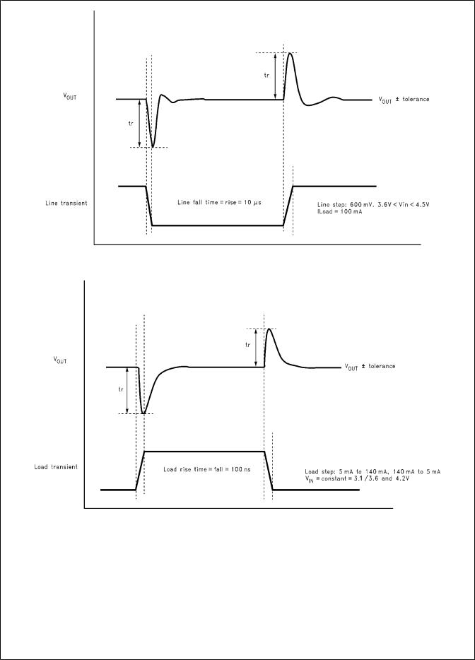
Note 8: Line Transient response requirement:
5 |
www.national.com |
LP3987
20022206
Note 9: Load Transient response requirement:
20022207
Note 10: All limits are guaranteed. All electrical characteristics having room-temperature limits are tested during production with TJ = 25°C. All hot and cold limits are guaranteed by correlating the electrical characteristics to process and temperature variations and applying statistical process control.
Note 11: The nominal output voltage, which is labeled VOUT(nom), is the output voltage measured with the input 0.5V above VOUT(nom) and a 1mA load. Note 12: During transient recovery, output voltage should not be oscillating.
Note 13: TON is measured from rising edge of Enable with MODE = 1.8V to when VOUT reaches 95% of final value.
Note 14: TSLEEP is measured from rising edge of Enable with MODE = 0V to when VOUT reaches 95% of final value.
Note 15: TMODE is measured from rising edge of MODE with ENABLE = 1.8V to time before full current capability.
www.national.com |
6 |
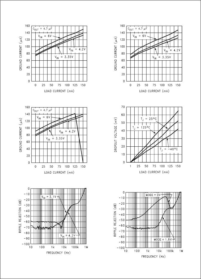
Typical Performance Characteristics Unless otherwise specified, CIN = COUT = 1 µF Ceramic, VIN = VOUT(nom) + 0.5V, TA = 25°C, Enable pin is tied to VIN, MODE = 1.8V.
Ground Current @ TA = 25°C |
Ground Current @ TA = 40°C |
20022228 |
20022226 |
Ground Current @ TA = 85°C |
Dropout Voltage vs Load Current |
20022227 |
20022229 |
Ripple Rejection (CIN = COUT = 1µF, IL = 1mA) |
Ripple Rejection (VIN = VOUT(nom) + 1V, |
|
CIN = COUT = 1µF, IL = 1mA) |
20022208
20022209
LP3987
7 |
www.national.com |

LP3987
TSLEEP @ MODE = 0V, COUT = 1µF, |
TSLEEP @ MODE = 0V, COUT = 1µF, |
IL = 1mA |
IL = 1mA |
20022213 20022214
TON @ MODE = 1.8V, COUT = 1µF, |
TON @ MODE = 1.8V, COUT = 1µF, |
IL = 150mA |
IL = 150mA |
20022215 20022216
TSLEEP @ MODE = 0V, COUT = 4.7µF, |
TSLEEP @ MODE = 0V, COUT = 4.7µF, |
IL = 1mA |
IL = 1mA |
20022217 |
20022218 |
www.national.com |
8 |

TON @ MODE = 1.8V, COUT = 4.7µF, |
TON @ MODE = 1.8V, COUT = 4.7µF, |
IL = 150mA |
IL = 150mA |
20022219 20022220
TMODE Measurement @ VIN = 3.05V TMODE Measurement @ VIN = 3.6V
20022225 20022224
TMODE Measurement @ VIN = 4.2V Output Short Circuit Current
20022223 |
20022222 |
LP3987
9 |
www.national.com |

LP3987
Output Short Circuit Current |
Load Transient Response @ VIN = 3.1V |
20022221 20022273
Load Transient Response @ VIN = 3.35V Load Transient Response @ VIN = 3.6V
20022230 20022231
Load Transient Response @ VIN = 4.2V Load Transient Response @ VIN = 3.1V, COUT = 1µF
20022232 |
20022272 |
www.national.com |
10 |