PC-POWER / FSDM311_FAIR
.pdf
FSDM311
|
|
|
OSC |
|
|
|
5uA |
400uA |
+ |
S |
Q |
GATE |
|
Vfb |
|
R |
|
DRIVER |
||
|
- |
|
|
|
||
4 |
|
|
|
|
|
|
|
R |
3V |
|
|
|
|
Cfb |
|
OLP |
|
|
|
|
|
|
|
|
|
||
|
|
|
|
S |
Q |
|
RESET |
Vth 4.5V |
|
R |
|
FSDM311 |
|
TSD |
|
OLP, TSD |
||||
A/R |
|
|||||
|
|
|
|
|
|
Protection Block |
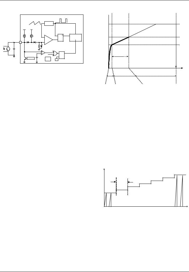
Figure 7. Protection block
4.1Over Load Protection (OLP) : Overload is a load current that exceeds a pre-set level due to an abnormal situation. If this occurs, the protection circuit should be triggered to protect the SMPS. It is possible that a short term load transient can occur under normal operation. If this occurs the system should not shut down. In order to avoid false shutdowns, the over load protection circuit is designed to trigger after a delay. Therefore the device can discriminate between transient overloads and true fault conditions. The device is pulse-by-pulse current limited and therefore, for a given input voltage, the maximum input power is limited. If the load tries to draw more than this, the output voltage will drop below its set value. This reduces the opto-coupler LED current which in turn will reduce the photo-transistor current. Therefore, the 400uA current source will charge the feedback pin capacitor, Cfb, and the feedback voltage, Vfb, will increase. The input to the feedback comparator is clamped at around 3V. Therefore, once Vfb reaches 3V, the device is switching at maximum power. At this point the 400uA current source is blocked and the 5uA source continues to charge Cfb. Once Vfb reaches 4.5V, switching stops. Therefore the shutdown delay time is set by the time required to charge Cfb from 3V to 4.5V with 5uA as shown in Fig. 5.
4.2Thermal Shutdown (TSD) : The Sense FET and the control IC are assembled in one package. This makes it easy
for the control IC to detect the temperature of the Sense FET. When the temperature exceeds approximately 145° C, thermal shutdown is activated.
Vfb
OLP 4.5V
3V


 FPS Switching Area
Idelay (5uA) charges Cfb |
IC Reset |
t
t1 |
t2 |
t3 |
t1<<t2, t3
t1 = -1/RCΧ ln( 1-v(t1)/R ) v(t1)=3V t2 = CΧ [v(t1+t2)-v(t1)]Χ Idelay
Figure 8. Over load protection delay
5. Soft Start : The FPS has an internal soft start circuit that increases the drain current limit together with the MOSFET current slowly after it starts up. The soft start time is typical 15msec as shown in figure 9. It progressively increases during the start-up phase. The pulse width to the power switching devices is progressively increased to establish the correct working conditions for transformers, inductors, and capacitors. The voltage on the output capacitors is progressively increased with the intention of smoothly establishing the required output voltage. Consequently it prevents the transformer’s saturation and the secondary diodes’s stress.
Drain current |
[A] |
.55A |
2mS |
7steps |
.31A |
t |
Figure 9. Internal Soft Start
11

FSDM311
6. Burst operation : In order to minimize the power dissipation in standby mode, the FSDM311 implements burst mode.
|
|
OSC |
|
|
|
|
S |
Q |
GATE |
5uA |
400uA |
R |
|
DRIVER |
|
|
|||
|
|
|
|
|
4 |
|
|
|
on/off |
Vfb |
|
|
|
|
|
|
|
0.70V |
|
|
|
|
/0.55V |
|
|
|
|
|
FSDM311 |
|
|
Burst operation Block |
||
Figure 10. Circuit for burst operation
As the load decreases, the feedback voltage decreases. The device automatically enters burst mode when the feedback voltage drops below VBURL(0.55V). At this point switching stops and the output voltages start to drop. This causes the feedback voltage to rise. Once is passes VBURH(0.70V) switching starts again. The feedback voltage falls and the process repeats. Burst mode operation alternately enables and disables switching of the power MOSFET to reduce the switching loss in the standby mode.
Vo
Vo set
V FB
0.7V
0.55V
Ids
Vds
time
Figure 11. Burst mode operation
12

FSDM311
Package Dimensions
8DIP
13

FSDM311
Package Dimensions (Continued)
8LSOP
14

FSDM311
Ordering Information
Product Number |
Package |
Marking Code |
Topr (° C) |
FSDM311 |
8DIP |
DM311 |
650V |
|
|
|
|
FSDM311L |
8LSOP |
DM311 |
650V |
|
|
|
|
15

FSDM311
DISCLAIMER
FAIRCHILD SEMICONDUCTOR RESERVES THE RIGHT TO MAKE CHANGES WITHOUT FURTHER NOTICE TO ANY PRODUCTS HEREIN TO IMPROVE RELIABILITY, FUNCTION OR DESIGN. FAIRCHILD DOES NOT ASSUME ANY LIABILITY ARISING OUT OF THE APPLICATION OR USE OF ANY PRODUCT OR CIRCUIT DESCRIBED HEREIN; NEITHER DOES IT CONVEY ANY LICENSE UNDER ITS PATENT RIGHTS, NOR THE RIGHTS OF OTHERS.
LIFE SUPPORT POLICY
FAIRCHILD’S PRODUCTS ARE NOT AUTHORIZED FOR USE AS CRITICAL COMPONENTS IN LIFE SUPPORT DEVICES OR SYSTEMS WITHOUT THE EXPRESS WRITTEN APPROVAL OF THE PRESIDENT OF FAIRCHILD SEMICONDUCTOR CORPORATION. As used herein:
1.Life support devices or systems are devices or systems which, (a) are intended for surgical implant into the body, or (b) support or sustain life, and (c) whose failure to perform when properly used in accordance with instructions for use provided in the labeling, can be reasonably expected to result in a significant injury of the user.
2.A critical component in any component of a life support device or system whose failure to perform can be reasonably expected to cause the failure of the life support device or system, or to affect its safety or effectiveness.
www.fairchildsemi.com
8/24/04 0.0m 0012004 Fairchild Semiconductor Corporation
