

PC-POWER / ML4800
.pdfPRODUCT SPECIFICATION |
ML4800 |
|
|
where C |
SSis the required soft start capacitance, and t |
DELAY |
||||||
is the desired start-up delay. |
|
|
|
|
||||
It is important that the time constant of the PWM soft-start |
|
|||||||
allow the PFC time to generate sufficient output power for |
|
|||||||
the PWM section. The PWM start-up delay should be at least |
|
|||||||
5ms. |
|
|
|
|
|
|
|
|
Solving for the minimum value of C |
: |
|
||||||
|
|
|
|
|
|
|
SS |
|
Css |
=5ms |
× |
25 µ |
A |
- |
= 100nF |
|
(6a) |
-------------- |
|
|
||||||
|
|
|
1.25V |
|
|
|
|
|
Caution should be exercised when using this minimum soft
start capacitance value because premature charging of the SS capacitor and activation of the PWM section can result if
V FB is in the hysteresis band of the V |
|
IN OK comparator at |
start-up. The magnitude of V |
FB at start-up is related both to |
|
line voltage and nominal PFC output voltage. Typically, a |
||
1.0µF soft start capacitor will allow time for V |
FB and PFC |
|
out to reach their nominal values prior to activation of the PWM section at line voltages between 90Vrms and 265Vrms.
Generating VCC
The ML4800 is a voltage-fed part. It requires an external 15V, ±10% (or better) shunt voltage regulator, or some other
V CC regulator, to regulate the voltage supplied to the part at 15V nominal. This allows low power dissipation while at the
same time delivering 13V nominal gate drive at the PWM OUT and PFC OUT outputs. If using a Zener diode for this
function, it is important to limit the current through the Zener to avoid overheating or destroying it. This can be easily done with a single resistor in series with the Vcc pin, returned to a bias supply of typically 18V to 20V. The
resistor’s value must be chosen to meet the operating current requirement of the ML4800 itself (8.5mA, max.) plus the current required by the two gate driver outputs.
EXAMPLE: |
|
|
|
|
|
|
|
With a V |
BIAS |
of 20V, a V CC |
of 15V and the ML4800 driving |
|
|||
a total gate charge of 90nC at 100kHz (e.g., 1 IRF840 |
|
||||||
MOSFET and 2 IRF820 MOSFETs), the gate driver current |
|
||||||
required is: |
|
|
|
|
|
|
|
I GATEDRIVE |
= 100kHz |
×90nC |
|
= 9mA |
(7) |
||
R BIAS |
V BIAS |
– V CC |
|
|
|
(8) |
|
= --------------------------------- |
+ I G + I Z |
|
|
|
|||
|
I CC |
|
|
|
|
||
|
|
20V –15V |
|
|
Ω |
|
|
R BIAS |
= 6mA-------------------------------------------------- |
+9mA 5mA+250 |
= |
|
|||
Choose R |
BIAS |
= 240Ω . |
|
|
|
|
|
The ML4800 should be locally bypassed with a 1.0µF ceramic capacitor. In most applications, an electrolytic
capacitor of between 47µF and 220µF is also required across the part, both for filtering and as part of the start-up bootstrap circuitry.
L1 |
|
SW2 |
I2 |
I3 |
|
|
|
|
|
|
|
I1 |
|
|
|
I4 |
|
+ |
|
|
|
|
|
VIN |
|
|
|
|
|
DC |
|
SW1 |
|
|
RL |
|
|
|
C1 |
|
|
REF + |
U3 |
|
|
|
|
EA |
|
|
|
|
|
– |
|
|
|
|
|
|
|
|
|
DFF |
|
RAMP |
+ |
|
R |
Q |
|
– U1 |
|
||||
OSC |
|
|
D U2 |
||
CLK |
|
|
|
Q |
|
|
|
|
|
|
|
U4 |
|
|
|
|
CLK |
|
|
|
|
|
|
RAMP |
VEAO |
TIME |
VSW1 |
TIME
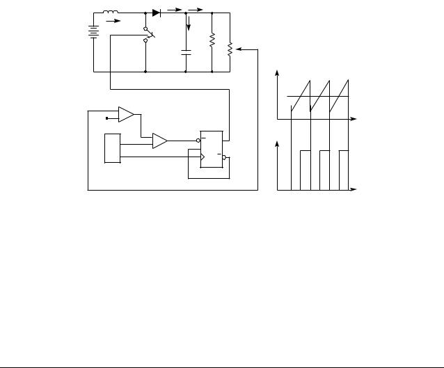
Figure 4. Typical Trailing Edge Control Scheme
REV. 1.0.5 9/25/01 |
11 |
ML4800 |
PRODUCT SPECIFICATION |
|
|
Leading/Trailing Modulation
Conventional Pulse Width Modulation (PWM) techniques employ trailing edge modulation in which the switch will turn on right after the trailing edge of the system clock. The error amplifier output voltage is then compared with the modulating ramp. When the modulating ramp reaches the
level of the error amplifier output voltage, the switch will be turned OFF. When the switch is ON, the inductor current will
ramp up. The effective duty cycle of the trailing edge modulation is determined during the ON time of the switch. Figure 4 shows a typical trailing edge control scheme.
In the case of leading edge modulation, the switch is turned OFF right at the leading edge of the system clock. When the
modulating ramp reaches the level of the error amplifier output voltage, the switch will be turned ON. The effective duty-cycle of the leading edge modulation is determined dur-
ing the OFF time of the switch. Figure 5 shows a leading edge control scheme.
One of the advantages of this control technique is that it requires only one system clock. Switch 1 (SW1) turns off and switch 2 (SW2) turns on at the same instant to minimize the momentary “no-load” period, thus lowering ripple voltage generated by the switching action. With such synchro-
nized switching, the ripple voltage of the first stage is reduced. Calculation and evaluation have shown that the
120Hz component of the PFC’s output ripple voltage can be reduced by as much as 30% using this method.
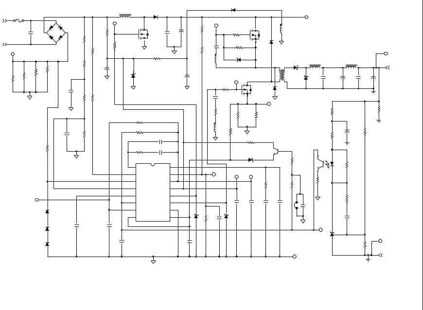
Typical Applications
Figure 6 is the application circuit for a complete 100W power factor corrected power supply, designed using the methods and general topology detailed in Application Note 33.
L1 |
|
SW2 |
I2 |
I3 |
|
|
|
|
|
|
|
||
I1 |
|
|
|
I4 |
|
|
+ |
|
|
|
|
||
VIN |
|
|
|
|
|
|
DC |
|
SW1 |
|
|
RL |
|
|
|
|
C1 |
|
|
|
+ |
U3 |
|
|
|
|
|
EA |
|
|
|
|
||
– |
|
VEAO |
|
|
|
|
REF |
|
|
DFF |
|||
|
|
+ CMP |
||||
RAMP |
R |
Q |
||||
– U1 |
|
|||||
OSC |
|
|
D U2 |
|||
CLK |
|
|
|
Q |
||
|
|
|
|
|
||
U4 |
|
|
|
|
CLK |
|
|
|
|
|
|
||
RAMP |
VEAO |
TIME |
VSW1 |
TIME
Figure 5. Typical Leading Edge Control Scheme
12 |
REV. 1.0.5 9/25/01 |
.REV |
|
9/25/01 5.0.1 |
100W .6 Figure |
|
33 Note Application Linear Micro Using Designed Supply, Power Corrected Factor Power |
13 |
|
|
|
|
|
|
|
|
|
D1 |
|
|
|
|
|
D12 |
|
|
|
|
|
|
|
|
|
|
|
|
|
|
|
|
|
|
8A |
|
|
|
|
|
|
|
|
|
|
|
|
|
|
|
|
|
|
|
|
|
|
L1 |
|
|
|
|
|
|
|
|
|
|
|
|
|
|
|
|
|
|
F1 |
|
|
|
|
|
FES16JT |
|
|
|
|
|
|
|
VBUSS |
|
|
|
|
|
|||||
|
|
|
|
|
|
|
|
|
|
|
|
|
|
|
|
|
|
|||||||
3.15A |
|
|
|
|
|
|
|
|
|
|
|
|
|
|
|
|
|
|
|
|
|
|
|
|
|
|
C1 |
BR1 |
|
|
Q1G |
|
|
|
|
C5 |
|
|
|
|
Q2 |
|
|
|
|
|
|
|
|
|
|
|
|
|
|
|
|
|
|
Q2G |
|
|
|
|
|
|
|
|
|
|
||||
|
|
4A, 600V |
|
|
|
|
|
|
100µ F |
|
R19 |
|
|
|
|
|
|
|
|
|
||||
AC INPUT |
|
0.47µ F |
|
|
IRF840A |
|
|
|
IRF820A |
T2C |
|
|
|
|
|
|
||||||||
|
KBL06 |
R27 |
|
|
|
|
|
33Ω |
|
|
|
|
|
|
|
|||||||||
|
|
|
|
|
|
|
|
|
|
|
|
|
|
|
|
|
|
|
|
|
||||
85 TO 260V |
|
|
|
R1 |
82kΩ |
|
|
Q1 |
|
C4 |
R13 |
|
|
|
|
|
|
|
|
|
|
|
|
|
|
|
|
|
|
|
|
|
|
383kΩ |
|
|
|
|
|
|
|
|
|
|
|
|
|||
|
|
|
|
357kΩ |
|
|
IRF840A |
4.7nF |
C25 |
R24 |
|
|
|
|
|
|
|
|
|
|||||
|
|
|
|
|
|
|
|
|
|
|
|
|
|
|
|
|||||||||
|
|
|
|
|
|
R20 |
|
|
|
|
|
|
0.1µ F |
10kΩ |
|
D5 |
|
|
|
|
|
|
|
|
|
|
|
|
|
R9 |
22Ω |
|
|
|
|
|
|
|
|
|
|
|
|
|
|
|
|
|
|
|
|
|
|
|
|
|
|
|
|
|
|
T1B |
|
|
|
600V |
|
|
|
|
|
|
||
ISENSE |
|
|
|
249kΩ |
|
|
|
|
|
|
R14 |
|
D7 |
|
|
|
|
|
|
|
|
12V |
||
|
|
|
|
|
|
|
|
|
|
|
|
|
|
|
|
|
|
|
||||||
|
|
|
|
R2 |
|
|
|
R28 |
|
|
383kΩ |
|
|
16V |
|
D11A |
L2 |
|
L3 |
|
|
|
||
|
|
|
|
|
|
|
|
|
|
|
|
|
|
|
|
|
|
|
||||||
|
|
|
|
357kΩ |
|
|
|
|
|
|
|
|
|
|
|
|
|
|
|
|||||
|
|
|
|
C26 |
|
|
240Ω |
|
|
|
|
|
|
|
|
|
|
|
|
|
|
12V, 100W |
||
|
|
|
|
|
|
|
|
|
|
|
|
|
|
|
|
|
|
|
|
|
|
|
||
|
|
|
R8 |
|
47µ F |
|
D2 |
|
|
|
C12 |
|
|
|
|
|
MBR2545CT |
|
|
|
|
|
|
|
|
|
|
|
|
|
|
|
|
|
|
|
|
|
|
|
|
|
|
|
|
||||
|
|
R7 |
1.2Ω |
|
|
|
15V |
|
|
|
|
Q3G |
|
|
|
|
|
|
|
|
|
|
||
|
R6 |
|
|
|
|
|
|
10µ |
F |
|
|
|
|
|
|
|
|
|
|
|
||||
R5 |
1.2Ω |
|
|
|
|
1N4744A |
|
|
R18 |
|
|
|
D11B |
C24 |
C21 |
C32 |
|
C30 |
|
|||||
1.2Ω |
|
|
|
|
|
|
|
|
|
35V |
33Ω |
|
|
IRF820A |
|
0.47µ F |
1500µ F |
0.47µ F |
1000µ F |
|
||||
1.2Ω |
|
|
|
|
|
|
|
|
|
|
|
|
|
|||||||||||
|
|
|
|
|
|
|
|
|
|
|
|
|
|
|
Q3 |
|
D6 |
|
|
|
|
|
|
|
|
|
|
|
|
|
|
|
|
|
|
|
|
|
|
|
|
|
|
|
|
|
|
||
|
|
|
C3 |
R3 |
R10 |
|
|
|
|
|
|
|
C20 |
|
|
|
|
600V |
|
|
|
|
|
|
|
|
|
0.22µ F |
|
|
|
|
|
|
|
|
|
|
|
|
|
|
|
|
|
|
|||
|
|
|
100kΩ |
249kΩ |
|
|
|
|
|
|
|
0.47µ |
F |
|
|
|
|
|
|
|
|
|
|
|
|
|
|
|
|
|
|
|
|
|
|
|
|
R17 |
|
|
|
PWM |
|
|
R29 |
|
|
|
R34 |
|
|
|
|
|
|
|
|
|
|
|
|
|
|
|
|
|
|
|
|
|
240Ω |
|||
|
|
|
|
|
|
|
|
|
|
|
|
|
|
|
|
ILIMIT |
|
|
|
|
|
|||
|
|
|
|
|
|
|
R38 |
|
|
|
|
|
3Ω |
|
|
|
|
|
1.2kΩ |
|
|
|
|
|
|
|
|
|
|
|
|
|
|
|
|
|
|
|
|
|
|
|
|
|
|
|
|||
|
|
|
|
|
|
|
42.2kΩ |
|
|
|
|
|
|
|
R21 |
R22 |
|
|
|
|
|
|
|
|
|
|
|
|
|
|
|
|
|
|
|
|
|
|
|
2.2Ω |
2.2Ω |
|
|
|
|
|
|
|
|
|
|
|
|
|
|
|
R16 10kΩ |
|
|
|
|
|
T1A |
|
|
|
|
|
|
|
C22 |
R32 |
|
|
|
|
|
|
|
|
|
|
|
|
|
|
|
|
|
|
|
|
|
|
R30 |
8.66kΩ |
|
||
|
|
|
|
|
|
|
|
|
|
|
|
|
|
R23 |
|
|
|
|
|
10µ |
F |
|
||
|
|
|
|
|
|
|
|
|
|
|
|
|
|
R37 1kΩ |
|
|
|
1.5kΩ |
|
|
||||
|
|
|
C2 |
R4 |
|
|
|
C7 150pF |
|
|
|
220Ω |
|
|
|
|
|
|
|
|||||
|
|
|
0.47µ F |
13.2kΩ |
|
|
|
|
|
|
|
|
|
|
|
|
|
2N3904 |
|
|
|
|
|
|
|
|
R39 |
|
|
|
|
|
C6 |
1.5nF |
|
|
|
|
|
|
|
|
|
|
|
|
|
||
|
|
33Ω |
|
|
|
|
R12 68.1k |
|
|
|
|
|
|
|
Q4 |
|
|
|
|
|
|
|||
|
|
|
|
|
|
|
|
|
|
|
|
|
|
D4 |
|
MOC8112 |
|
|
|
|
||||
|
|
|
|
|
|
|
|
|
|
|
|
|
|
|
|
|
|
|
|
|
|
|||
|
|
|
|
|
|
|
|
|
|
|
|
|
|
|
|
5.1V |
|
R25 |
|
U2 |
|
|
|
|
|
|
|
|
|
|
|
ML4800 |
|
|
|
|
|
|
|
|
|
|
|
|
|
|
|
||
|
|
|
|
|
|
|
|
|
|
|
|
|
1N4733A |
|
10kΩ |
|
|
R44 |
|
|
|
|||
|
|
|
|
|
|
|
1 |
|
|
|
16 |
|
|
|
|
|
|
|
|
|
||||
|
|
|
|
|
|
|
|
|
VDC |
|
|
|
|
|
|
|
10kΩ |
|
|
|
||||
|
|
|
|
|
|
|
|
|
|
|
|
|
|
|
|
|
|
|
|
|
||||
|
|
|
|
|
|
|
IEAO |
U1 |
|
|
|
VFB |
|
|
|
|
|
|
|
|
|
|
|
|
|
|
|
|
|
|
|
2 |
|
VFB |
15 |
|
VCC |
REF |
|
|
|
|
|
|
|
|
|||
|
|
|
|
|
|
|
|
|
|
|
|
|
|
|
|
|
|
|
||||||
|
|
|
|
|
|
|
IAC |
|
|
|
|
|
|
|
|
|
|
R40 |
|
|
|
|
||
|
|
|
|
|
|
|
3 ISENSE |
|
|
|
14 |
|
|
|
|
|
|
|
|
|
|
|
||
|
|
|
|
|
|
|
|
VREF |
|
|
|
|
|
R11 |
R26 |
470Ω |
|
|
|
|
||||
|
|
|
|
|
|
|
4 VRMS |
|
|
VCC |
13 |
|
|
|
|
|
412kΩ |
10kΩ |
|
|
|
|
|
|
|
|
RT/CT |
|
|
|
|
5 SS |
PFC OUT 12 |
|
|
|
|
|
|
J8 |
|
|
R31 |
|
|
|
|||
|
|
|
|
|
|
|
6 VDC |
PWM OUT 11 |
|
|
|
|
|
|
|
|
10kΩ |
|
|
|
||||
|
|
|
|
|
|
|
|
|
C15 |
C13 |
C8 |
C9 |
|
|
|
|
|
|||||||
|
|
|
|
|
|
|
7 RAMP1 |
|
|
GND |
10 |
D8 |
C31 |
1.0µ F |
0.22µ F |
150µ F |
15nF |
C10 |
|
|
|
|
|
|
|
|
|
D14 |
|
|
|
8 |
|
|
|
9 |
330pF |
D10 |
|
|
|
|
10µ F |
|
C23 |
|
|
||
|
|
|
|
|
|
RAMP 2 |
DC ILMIT |
|
|
|
|
|
|
|
|
|
|
|
|
|||||
|
|
|
1N914 |
|
|
|
|
|
|
|
|
|
|
|
|
|
10nF |
|
|
|||||
|
|
|
|
|
|
|
|
|
|
|
|
|
R15 |
|
|
|
|
|
VDC |
|
|
|
|
|
|
|
|
|
C19 |
|
C18 |
|
|
|
|
|
|
4.99kΩ |
|
|
|
|
|
|
|
|
|
||
|
|
|
|
|
|
|
|
|
|
|
|
|
|
|
|
|
|
|
|
|
|
|
||
|
|
|
D13 |
1.0µ F |
|
470pF |
|
|
|
|
|
|
|
|
|
|
|
|
|
U3 |
|
|
|
|
|
|
|
1N914 |
|
|
|
|
|
|
|
|
|
|
|
|
|
|
|
|
|
|
|
|
|
|
|
|
|
|
|
|
|
|
|
|
|
|
|
|
|
|
|
TL431A |
|
|
|
|
||
|
|
|
|
|
|
|
|
|
|
|
|
|
|
|
|
|
|
|
|
|
|
12V RET |
||
|
|
|
|
|
|
C11 |
|
|
|
|
|
|
|
|
|
|
|
|
|
|
|
R33 |
|
|
|
|
|
D15 |
|
|
|
|
|
|
|
C28 |
|
|
|
|
|
|
|
|
2.26kΩ |
|
|
||
|
|
|
|
|
220pF |
|
|
|
220pF |
|
|
|
|
|
PRI GND |
|
|
|
|
|
|
|||
|
|
|
1N914 |
|
|
|
|
|
|
|
|
|
|
|
|
|
|
|
|
|
|
|
12V |
|
|
|
|
|
|
|
|
|
|
|
|
|
|
|
|
|
|
|
|
|
|
|
|
|
RETURN |
NOTE: |
D7, D8, D10; 1N966B |
|
|
|
|
|
|
|
|
|
|
|
|
|
|
|
|
|
|
|
|
|
||
|
|
D3, D5, D6, D12; UF4005 |
|
|
|
|
|
|
|
|
|
|
|
|
|
|
|
|
|
|
|
|
|
|
|
|
D4; 1N4733A |
|
|
|
|
|
|
|
|
|
|
|
|
|
|
|
|
|
|
|
|
|
|
|
|
D2; 1N4744A |
|
|
|
|
|
|
|
|
|
|
|
|
|
|
|
|
|
|
|
|
|
|
|
|
D11; MBR2545CT |
|
|
|
|
|
|
|
|
|
|
|
|
|
|
|
|
|
|
|
|
|
|
|
|
L1; PREMIER MAGNETICS TSD-1047 |
|
|
|
|
|
|
|
|
|
|
|
|
|
|
|
|
|
|
|
|
||
|
|
L2; PREMIER MAGNETICS VTP-05007 |
|
|
|
|
|
|
|
|
|
|
|
|
|
|
|
|
|
|
|
|
||
|
|
L3; PREMIER MAGNETICS TSD-904 |
|
|
|
|
|
|
|
|
|
|
|
|
|
|
|
|
|
|
|
|
||
|
|
T1; PREMIER MAGNETICS PMGD-03 |
|
|
|
|
|
|
|
|
|
|
|
|
|
|
|
|
|
|
|
|
||
|
|
T2; PREMIER MAGNETICS TSD-735 |
|
|
|
|
|
|
|
|
|
|
|
|
|
|
|
|
|
|
|
|
||
|
|
UNUSED DESIGNATORS; C14, C16, C17, C27, C29, C33, D3, D9, R42, R43, R36, R35 |
|
|
|
|
|
|
|
|
|
|
|
|
|
|
||||||||
SPECIFICATION PRODUCT
ML4800

ML4800 PRODUCT SPECIFICATION
Ordering Information
Part Number |
Temperature Range |
Package |
|
|
|
ML4800CP |
0°C to 70°C |
16-Pin PDIP (P16) |
|
|
|
ML4800CS |
0°C to 70°C |
16-Pin Narrow SOIC (S16N) |
|
|
|
ML4800IP |
-40°C to 85°C |
16-Pin PDIP (P16) |
|
|
|
ML4800IS |
-40°C to 85°C |
16-Pin Narrow SOIC (S16N) |
|
|
|
DISCLAIMER
FAIRCHILD SEMICONDUCTOR RESERVES THE RIGHT TO MAKE CHANGES WITHOUT FURTHER NOTICE TO ANY PRODUCTS HEREIN TO IMPROVE RELIABILITY, FUNCTION OR DESIGN. FAIRCHILD DOES NOT ASSUME ANY LIABILITY ARISING OUT OF THE APPLICATION OR USE OF ANY PRODUCT OR CIRCUIT DESCRIBED HEREIN; NEITHER DOES IT CONVEY ANY LICENSE UNDER ITS PATENT RIGHTS, NOR THE RIGHTS OF OTHERS.
LIFE SUPPORT POLICY
FAIRCHILD’S PRODUCTS ARE NOT AUTHORIZED FOR USE AS CRITICAL COMPONENTS IN LIFE SUPPORT DEVICES OR SYSTEMS WITHOUT THE EXPRESS WRITTEN APPROVAL OF THE PRESIDENT OF FAIRCHILD SEMICONDUCTOR CORPORATION. As used herein:
1.Life support devices or systems are devices or systems which, (a) are intended for surgical implant into the body, or (b) support or sustain life, or (c) whose failure to perform when properly used in accordance with instructions for use provided in the labeling, can be reasonably expected to result in significant injury of the user.
2.A critical component is any component of a life support device or system whose failure to perform can be reasonably expected to cause the failure of the life support device or system, or to affect its safety or effectiveness.
www.fairchildsemi.com
9/25/01 0.0m 001 Stock#DS300048002001 Fairchild Semiconductor Corporation