

dsd13-gos / dsd-14=pdk / Lect09_10
.pdfTitle: Introduction to Components Description Format (CDF)
Date:
Author:
1 CADENCE DESIGN SYSTEMS, INC.

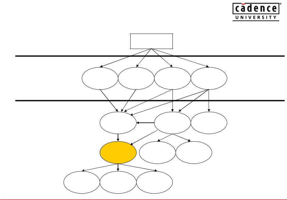
PDK Data Map
USER
CADENCE
PDK
Chip Designer
Schematic |
Simulation |
Layout |
Verification |
|
capture |
||||
|
|
|
Symbols |
Device |
Verification |
|
Layouts |
Rule Files |
||
|
CDF |
Techfile |
VXL Env |
Params |
SimInfo |
Callbacks |
3 |
CADENCE CONFIDENTIAL |

What Is CDF?
The Component Description Format (CDF) describes the parameters and the attributes of parameters of individual components and libraries of components.
4 |
CADENCE CONFIDENTIAL |

CDF purposes
•Assigning parameter names and values
•Allocating units and default values
•Checking that values lie within specified ranges
•Dynamically changing how parameters are displayed depending on predefined conditions
•Executing a SKILL callback function whenever certain information is changed
5 |
CADENCE CONFIDENTIAL |

CDF benefits
•a single location for storing all component information so that applications can share and reuse parts of the component description.
•independence from applications and cellviews.
•a graphical user interface (the Edit Component CDF form) for entering and editing component information.
•strict checking so that tools do not need to check component data before using it.
•basic units and scale factors that are common in electrical design.
•a modular format, so that you can edit and update parts of a description.
•a command to copy the CDF description of one component into another component.
6 |
CADENCE CONFIDENTIAL |

A Typical Application
•You can choose how to specify the thin film resistivity by specifying the resistivity as a sheet resistance (ohms per square)
•Specifying the bulk resistivity of the material
If you want an ideal resistor, you specify the value of resistance desired. If you want a thin-film resistor, which models discontinuities as well as skin and substrate effects, you specify the length and width of the resistor and the resistivity of the material in which the resistor body is built.
7 |
CADENCE CONFIDENTIAL |
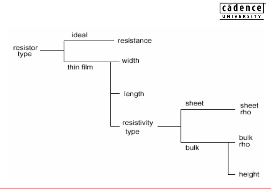
A Typical Application (cont.)
8 |
CADENCE CONFIDENTIAL |

Schematic Symbols & CDFs
•Cadence’s “analogLib” should be used for symbol templates.
•By using this standard, migration between PDKs will be easier.
The most common place to get symbol templates is from the Cadence “analogLib”. This library can be located in the Cadence DFII hierarchy at “$CDSHOME/tools/dfII/etc/cdslib/artist/analogLib”. By using this common source as a template, migrating schematics from one PDK to another becomes a much easier process.
9 |
CADENCE CONFIDENTIAL |

CDF’s types
There are two types of CDF’s:
The first is the library CDF
The library CDF, when set, can control two important items. The first item which can be set in the library CDF is the schematic display values. The second item which can be set in the PDK library CDF is the component types used for chaining and folding in Virtuoso XL.
The second is the cell CDF
The device CDF is used to set parameter names, parameter units, parameter types, default values, and Cadence internal properties (callback, parsing, etc). Once this device CDF is loaded, the resulting Edit Object Properties Form will be created for the nmos device:
10 |
CADENCE CONFIDENTIAL |