

dsd11-12 / dsd-12=Проектирование РЧ КМОП ИС / papers / 96_HF_Variable-Gain_Amplifire
.PDFIEEE JOURNAL OF SOLID-STATE CIRCUITS, VOL. 31, NO. 7, JULY 1996 |
1029 |
Brief Papers
CMOS Low-Distortion High-Frequency Variable-Gain Amplifier
J. J. F. Rijns
AbstractÐ The overall system performance of mixed-signal CMOS IC's is largely determined by the dynamic performance of the analog front-ends. System features are, in contrast, mainly set by the digital architecture. In order to optimize the dynamic range of the system and to minimize the sensitivity to substrate noise, the analog-to-digital converter (ADC) has to be preceded by a variable-gain amplifier (VGA) and a differential circuit topology for the complete front-end to be adopted. Since most of present-day applications are based on single-sided signal source definitions, the differential-input VGA must be able to perform a single-to-differential signal conversion. This paper describes the principle and design of a differential CMOS low-distortion variable-gain amplifier for high-frequency (video) applications. Experimental results of the circuit show total harmonic distortion
figures better than |
60 dB and a gain accuracy of 0.05 dB over |
the 2 to +12 dB gain range for single-sided input signals. |
|
|
I. INTRODUCTION |
UTOMATIC gain control (AGC) circuits are most often |
|
Aused in audio |
and video mixed-signal IC's in order |
to maximize the dynamic range of the overall system. The specifications for the linearity of the analog variable-gain amplifier (VGA) forming the core of these circuits are generally very high, to prevent limiting of the overall harmonic distortion by the AGC itself. When used in combination with an analog-to-digital converter (ADC) on a mixed analogdigital system IC, a differential or balanced circuit topology of the VGA-ADC combination is to be preferred from crosstalk perspective [1]. Balancing of the front-end up to the bondpad impedances expands this concept even from die to device level. These statements also hold for unbalanced system definitions, e.g., video of the present-day. In these applications, the differential variable-gain amplifier needs to perform a single-to-differential conversion of the analog input signal. The reverse signal conversion is done by the differential ADC in the digital domain after the crosstalk-sensitive analog comparator operations, see Fig. 1. In order to emphasize the dual mode operation (single-sided or differential inputs), an analog conversion stage is modeled in front of a differential VGA. Furthermore, convenient interfacing to the outside world is obtained by requiring high-ohmic inputs for the circuit. This paper describes the design and measurement results of a differential video amplifier with a 3-b programmable gain and attenuation range in a standard 0.8  m CMOS
Manuscript received November 21, 1995; revised February 9, 1996.
The author was with Philips Research Laboratories, 5656 AA Eindhoven, The Netherlands. He is now with Philips Semiconductors Communications & Multimedia, 6534 AE Nijmegen, The Netherlands.
Publisher Item Identifier S 0018-9200(96)04461-7.
technology. Measurement results are reported for single-sided input sources, since this is the most common but also most severe mode of application.
II. CIRCUIT PRINCIPLE AND DESIGN
This section describes the design of a differential video amplifier with a programmable gain and attenuation range. The architectural choices and various design issues are discussed separately.
A. Differential Variable-Gain Amplifier Architecture
A standard topology for a differential variable-gain amplifier is a degenerated differential pair with a resistive load as shown in Fig. 2. The differential input voltage signal 
 is copied over the series impedance of the two nonlinear transconductances
 and the linear (Poly-Si) degeneration
resistor |
resulting in a differential signal current |
||||
given by |
|
|
|
|
|
|
|
|
|
|
(1) |
|
|
|
|
||
|
|
|
|
|
|
A major advantage of this open-loop VGA architecture over the commonly used closed-loop variable-feedback architecture is that the amplifier can be designed to produce both gain and attenuation by means of the ratio of load and degeneration resistors. For high-frequency applications, wide-band noise specifications limit the value of the degeneration and load resistors to the 
 range. Practical values for the transconductance of the differential pair are limited to the mA/V range for modern CMOS processes. As a first consequence of the limited range for these resistors values, the degeneration gain will be relatively low, e.g., 1±10 times, resulting in a moderate gain accuracy and linearity of the voltage-to-current (VI) conversion. The amplifier gain can be selected either by using a variable degeneration or load resistor. In order to realize an amplifier bandwidth independent of the programmable amplifier gain, the poles at the VGA output nodes have to be kept constant. A variable degeneration resistor is therefore mostly preferred as programmable impedance in the VGA. A variable degeneration resistor can be created using a resistor bank or ladder with CMOS switches to obtain selectable taps. A second consequence of the limited range for the degeneration resistor's values relates to the practical implementation of these selector switches, which have nonlinear on-resistances limited to the 100
  region and will therefore have a nonnegligible influence on the conversion
0018±9200/96$05.00 ã 1996 IEEE

1030 |
IEEE JOURNAL OF SOLID-STATE CIRCUITS, VOL. 31, NO. 7, JULY 1996 |
Fig. 1. Front-end for mixed-signal IC's.
Fig. 2. Basic differential VGA architecture: degenerated differential pair |
|
with resistive loads. |
Fig. 5. Interpolated ±2 ladder. |
Fig. 3. Concept VGA with linear variable VI converter core.
Fig. 4. Current-driven R± |
ladder and Norton equivalent. |
impedance. This effect also results in a moderate gain accuracy and linearity.
B. Degenerated Differential Pair with
Transconductance Enhancement
The degeneration gain of the circuit can be enhanced by boosting the transconductances with the use of additional floating amplifiers [2] or with grounded amplifiers [3]. Apart from the ease of implementation and power considerations, it will be shown that the use of grounded 
 -boosting amplifiers
can be combined with a low-distortion switch technique [4], [5]. Fig. 3 shows the concept of the degenerated differential pair with grounded 
 -boosting amplifiers. With the use of the two NMOS transistors acting as gain stages, the PMOS input devices are forced to conduct a static current
  . As a result, these input devices ideally act as dc level shifters, creating a linear voltage copy of the input signals from gate to source. The NMOS gain transistors conduct a dc current


 plus the ac signal current
  which is determined by the differential voltage input and the conversion impedance


 . This conversion impedance is that part of the total degeneration resistor
  which is connected in between the feedback nodes 1 and 2 of the gain stages as illustrated in the figure. A variable conversion impedance is easily implemented by tapping-off the degeneration resistor to the gain feedback nodes with the use of simple NMOS selector switches. Since these switches operate in series with the NMOS current feedback transistors, their strongly nonlinear on-resistances form no part of the conversion impedance and will therefore have no effect on the linearity of the VI conversion. The linearized differential signal current can easily be copied out by loading nodes 3 and 4 with two matched NMOS devices as shown in Fig. 3. Clearly, the grounded amplifiers only apply a finite gain to the differential pair. The small signal open-loop gain
 of these transconductance amplifiers is the product of their transconductances times the impedances at the output nodes 3 and 4. Including these finite open-loop gains
 , the VI conversion gain of the degenerated differential pair with grounded
 -boosting amplifiers yields
(2)

IEEE JOURNAL OF SOLID-STATE CIRCUITS, VOL. 31, NO. 7, JULY 1996 |
1031 |
Fig. 6. Circuit implementation variable-gain amplifier.
TABLE I
EXPERIMENTAL PERFORMANCE SUMMARY
Fig. 7. Die photograph.
This equation shows that the additional gain 
 creates an accurate VI conversion gain, primarily determined by the linear degeneration resistor, resulting in low harmonic distortion. The nondominant pole of the additional amplifiers is found at the source nodes of the PMOS input devices. Stability is determined by the dominant pole locations at the closed-loop amplifiers input/output node impedances 3 and 4. In Section III, the influence of the finite bandwidth of the amplifiers on the harmonic distortion will be discussed.
C. Programmable Conversion Impedance
As explained in Section II-A, the variable gain of the differential amplifier is preferably implemented using a variable degeneration and a constant load resistor, since this choice results in a constant pole at the VGA output nodes. The 
 - boosted PMOS input devices of the VGA create a copy of the differential input voltage signal over the variable degeneration resistor. However, the ac signal current required to sustain this voltage copy is supplied from a variable tap on this resistor. For our application, a programmable logarithmic gain distribution is specified with eight steps of 2 dB ranging from
2 to  12 dB. Fig. 5 shows an interpolated
  ±
±
 ladder
network with eight taps used for this specification. As is known from current-steering DA converters,  ±
±
 ladders networks can be used to create a binary weighted sum of currents [6]. Fig. 4 illustrates the Norton equivalent of a threesection current driven
  ±
±
 ladder consisting of an impedance
  loaded with a single binary weighted sum current. When using this
  ±
±
 ladder as one half of the degeneration resistor in the VGA, the input signal is copied over the ladder input impedance
  and the ac signal current is supplied from one of the three main ladder nodes. The binary current scaling effect of the
  ±
±
 ladder for the current-driven application is converted into a binary impedance scaling effect for this voltage-driven application. Extending this concept, the Norton equivalent of the interpolated
  ±
±
 ladder of Fig. 5 can be found as an input impedance
  (
( is normalized to unity in Fig. 5) with a total load current


(3)

1032 |
IEEE JOURNAL OF SOLID-STATE CIRCUITS, VOL. 31, NO. 7, JULY 1996 |
Fig. 8. Measured gain responses.
Fig. 9. Measured HD2 for single-sided inputs, 1- |
output. |
assuming input currents |
passed by the selection switches |
|||
– . This |
equation shows that the sum |
current |
||
consists of a |
scaled |
version |
of these input |
currents |
. In this application, only |
a single |
ladder input current |
||
is selected simultaneously, which relates to the VGA output signal and load resistor 


 . Dependent on the selected ladder node, the logarithmically scaled replica of this
current |
equals the required |
ac |
ladder input current |
|
signal |
. A logarithmic gain distribution |
|
||
is obtained, |
which is scalable with |
the |
ratio of |
and |
. The main ladder switches |
|
, and |
select the |
|
0, 6, and 12 dB gain settings. The intermediate 2 dB gain
steps are closely approached by interpolation with the use of 3/12, 4/12, and 5/12 unit resistor fractions (


 dB,
dB, 


 dB). Apart from the interpolated
  ±
±
 ladder, an embedded 3-b binary to 1-b high decoder has been designed to drive the NMOS gain selector switches.
D. Circuit Implementation Variable-Gain Amplifier
The implementation of the variable-gain amplifier is shown in Fig. 6. The degenerated differential pair is biased using high-compliance dc current sources. Distribution of the total bias current has been adopted in order to obtain a maximum common-mode input signal range and an acceptable noise
IEEE JOURNAL OF SOLID-STATE CIRCUITS, VOL. 31, NO. 7, JULY 1996 |
1033 |
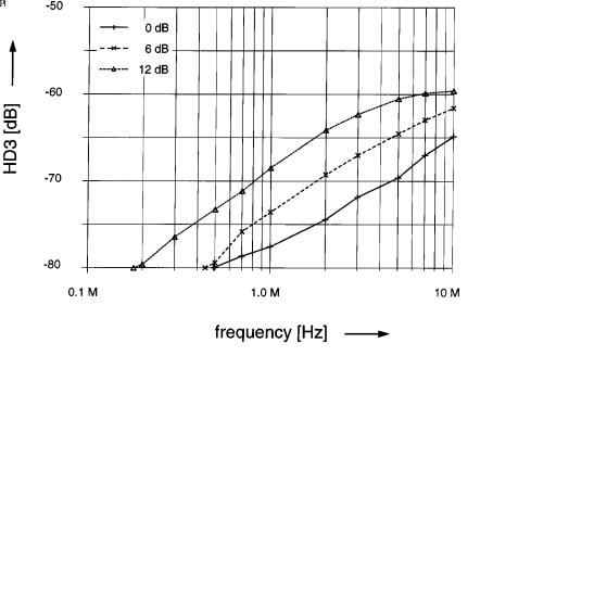
Fig. 10. Measured HD3 for single-sided inputs, 1- |
output. |
behavior. Tradeoffs between the dc voltage drop over the degeneration resistor and the contribution of the dc current sources to the overall noise level have been made. At the  rail, the grounded gain-boosting amplifiers are implemented using active cascodes in order to maximize the output impedance. The effect of the finite output impedances leads to modulation of the total bias current and therefore affects the gain accuracy and linearity. A constant current is added to the two output load resistors to generate a convenient commonmode output signal. The accuracy of this common-mode output signal level will be determined by the process spread of the linear poly-Si load resistors and the accuracy of the reference bias current. This accuracy can be enhanced by adopting a more elaborate biasing scheme. A reference voltage level (e.g., mid-range of ADC input following the VGA) can be copied to an additional resistor which is matched to the degeneration and load resistors. A process dependent bias current is obtained in this way which can be used for the biasing of the output resistor loads.
III. EXPERIMENTAL RESULTS
The variable-gain amplifier is realized in a 0.8  m CMOS technology. Both load and
  ±
±
 ladder resistors are realized using 1200
  linear poly-Si strips. Fig. 7 shows a die photograph of the 0.175 mm
 design. The power consumption of the complete circuit is 25 mW from a single 5-V supply. A summary of the experimental performance is listed in Table I.
A. Gain Response
The single-to-differential gain responses for all eight gain settings are shown in Fig. 8. The overall gain accuracy based on more than 100 measurements equals 0.05 dB 

 , which corresponds to the theoretical matching properties of the polySi resistors. The bandwidth of the VGA is limited by the 7 pF
probe to 15 MHz. The intrinsic bandwidth is determined by the bandwidth of degeneration network including the source impedances of the PMOS input devices and the capacitive load formed by the selector switches. Measurement of the VGA with low-ohmic termination shows an intrinsic bandwidth exceeding 60 MHz.
B. Harmonic Distortion
The harmonic distortion behavior of the variable-gain amplifier is evaluated for single-sided inputs for three different gain settings of 0, 6, and 12 dB. The differential output signal level is set to  -
- for all measurements. Fig. 9 shows that the second-order harmonic distortion scales proportional to the input signal level for frequencies up to the low megahertz range. The finite impedances at the variable current feedback nodes cause an input signal dependent modulation of the bias currents when the VGA is driven from a single-sided source. This asymmetrical effect causes even-order harmonic distortion and is not affected by the additional gain of the boosting amplifiers. At higher frequencies, the second-order harmonic distortion is asymptotically limited by the finite matching of the two output stages. As mentioned in the previous section, the bandwidth of the boosting amplifiers has to be limited by capacitive loading at the amplifiers output nodes to guarantee stability, since the nondominant pole locations of the total VGA are fixed. The voltage signal level at these nodes is determined by the boosting amplifier gain and the VGA output signal level. The finite channel matching therefore results in a capacitive bias current modulation which is a function of the VGA output signal level and the boosting amplifier gain. Driving the VGA from a differential source balances this current modulation effect caused by the finite current feedback node impedances. The finite matching accuracy of the output stages practically limits the second-harmonic distortion to the asymptotic limit mentioned above. Fig. 10 shows the third-

1034 |
IEEE JOURNAL OF SOLID-STATE CIRCUITS, VOL. 31, NO. 7, JULY 1996 |
Fig. 11. Measured THD for single-sided inputs, 1- |
output. |
order harmonic distortion behavior, again for three different gain settings and a differential output signal level set to  -
- . This graph shows that the third harmonic distortion is inversely proportional to the input signal level. The odd-order distortion is a function of the modulation index of the PMOS input pair. Since these measurements have been made using a constant output signal level, the ac signal current level and therefore the ac gate-source voltage modulation of the input pair is constant. Since the modulation index determines the distortion, the third-order harmonic distortion is inversely proportional to the input signal level. Fig. 11 shows that the experimental total harmonic distortion figures are below 60 dB up to the low megahertz range for single-sided input operation. The total output-referred inband noise level is 325


 . The VGA thereby meets the dynamic range requirements for 10-b analog-to-digital converter applications.
IV. CONCLUSION
A merged gain enhancement and low-distortion switch technique is successfully implemented in a differential variablegain video amplifier in a standard 0.8  m CMOS technology. The versatile amplifier can be driven from a single-sided or a differential input signal source and can produce both gain and attenuation. Experimental total harmonic distortion (THD)
figures below 60 dB are obtained in the megahertz range for single-sided input operation. The THD behavior and the inband noise level of 325  V
V

 make the amplifier suitable for use in an AGC for 10-b analog-to-digital converter applications. The gain accuracy of the circuit is better than 1% and is determined by the matching properties of on-chip poly-Si resistors. Further extension of the number of gain steps is possible since the intrinsic bandwidth of the amplifier exceeds the overall bandwidth in the presented realization.
REFERENCES
[1]K. Makie-Fukuda et al., ªMeasurement of digital noise in mixed-signal integrated circuits,º IEEE J. Solid-State Circuits, vol. 30, no. 2, pp. 87±91, Feb. 1995.
[2]R. J. van de Plassche, ªA wide-band monolithic instrumentation amplifier,º IEEE J. Solid-State Circuits, vol. SC-10, pp. 424±431, Dec. 1975.
[3]S. D. Willingham et al., ªA BiCMOS low-distortion 8-MHz low-pass filter,º IEEE J. Solid-State Circuits, vol. 28, no. 12, pp. 1234±1245, Dec. 1993.
[4]J. J. F. Rijns, ªCMOS low-distortion high-frequency variable-gain amplifier,º in IEEE ESSCIRC Dig. Tech. Papers, Sept. 19±21, 1995, pp. 46±49.
[5] , ªLow-distortion switch technique for variable gain circuits,º patent pending.
[6]D. J. Dooley, ªA complete monolithic 10-b D/A converter,º IEEE J. Solid-State Circuits, vol. SC-8, pp. 404±408, Dec. 1973.