

Статьи на перевод PVDF_P(VDF-TrFE) / Crystallization and microstructure-dependent elastic moduli of ferroelectric P(VDF–TrFE) thin films
.pdfDownloaded by Stanford University on 24 February 2013 |
Published on 20 September 2010 on http://pubs.rsc.org | doi:10.1039/C0SM00350F |
View Article Online / Journal Homepage / Table of Contents for this issue
PAPER |
www.rsc.org/softmatter | Soft Matter |
|
|
Crystallization and microstructure-dependent elastic moduli of ferroelectric P(VDF–TrFE) thin films†‡
Si-Woo Hahm and Dahl-Young Khang*
Received 10th May 2010, Accepted 19th July 2010
DOI: 10.1039/c0sm00350f
The crystallization behaviour of ferroelectric P(VDF–TrFE) copolymer thin films on various substrates has been investigated. The substrates used include bare Si for a high energy surface, and fluorinated self-assembled monolayer deposited Si and elastomer PDMS for low energy surfaces. Low energy surfaces have been found to enhance the crystallization rate. Additionally, the elastic moduli of those thin films, having thicknesses ranging from 30 nm to 1 mm, have been determined by the buckling method. The moduli have been found to depend strongly on the films microstructure, and have shown a maximum at the crystallization temperatures of 120 C–140 C. The films annealed at these temperatures show more than a 5 increase in modulus than that of the room-temperature dried ones. The dependence of the modulus on the film microstructure has been found to be closely related to the change in film crystallinity. The measured moduli of P(VDF–TrFE) thin films can help with the design and practical implementation of emerging applications such as flexible nonvolatile memories and piezoelectric energy harvesting devices.
1. Introduction
Ferroelectric polymer polyvinylidene fluoride–trifluoroethylene (P(VDF–TrFE)), which is a random copolymer of vinylidene fluoride (–CH2–CF2–) and trifluoethylene (–CHF–CF2–) units, has been used in a variety of applications,1 ranging from electromechanical transducer to biomedical sensors and actuators, etc. This is because the trifluoroethylene unit allows the resulting copolymer to adopt the all-trans conformation and unit cell of the ferroelectric b phase, in contrast to the existence of polymorphism (a, b, g, d) in the homopolymer PVDF. The all-trans b phase is known to have a net dipole and piezoelectric property. Recently, P(VDF–TrFE) has found novel applications such as in flexible non-volatile memory devices2,3 and piezoelectric energy harvesting approaches.4 In these emerging applications, P(VDF– TrFE) is usually applied in thin film or electrospun fiber forms, contrary to existing applications that use rather thick (> 10 mm) films. Further, in flexible memory devices and electromechanical energy conversion applications, the mechanical properties, especially the Young’s modulus, is one of the fundamental material properties to be considered and used for the optimized fabrication/operation of devices. For example, accurate
Department of Materials Science and Engineering, Yonsei University, 262 Seongsanno, Seodaemun-gu, Seoul, 120-749, Korea. E-mail: dykhang@ yonsei.ac.kr; Fax: +82-2-312-5375; Tel: +82-2-2123-5835
† Electronic supplementary information (ESI) available: S1) Crystalline morphology of P(VDF–TrFE) thin films on various substrates at low temperatures. S2) Buckling wavelengths of P(VDF–TrFE) thin films, prepared and annealed on FSAM-treated Si substrate (a) and on PDMS (b). S3) Tabulated moduli values of P(VDF–TrFE) thin films, with % crystallinity data from the literature. S4) Elastic moduli and % crystallinity of P(VDF–TrFE) thin films as a function of annealing/crystallization temperature. S5) Elastic moduli of PDMS as a function of curing temperature by micro-tensile test. S6) Optimization of FSAM treatment on Si substrate. See DOI: 10.1039/c0sm00350f/
‡ This paper is part of a Soft Matter themed issue on The Physics of Buckling. Guest editor: Alfred Crosby.
information on the mechanical behavior of constituent materials is essential in designing and implementing electronic devices that experience mechanical deformation during fabrication and in active service. The mechanical modulus of piezoelectric materials in electromechanical energy conversion devices is directly related to the elastic strain energy, where the stored elastic energy is linearly dependent upon the modulus.
Meanwhile, the Young’s modulus value of P(VDF–TrFE) covers a wide range of values in the existing literature,5–10 ranging from below GPa to over 100 GPa. Furthermore, those data were obtained for rather thick (thicker than 10 mm) films. Therefore, a simple and easy method for the characterization of the mechanical modulus of a P(VDF–TrFE) thin film is essential for the success of emerging novel applications mentioned previously. In general, it is hard to measure the mechanical properties of materials in thin (<1 mm) film form, because one cannot apply a traditional tensile test setup for such a sample. In this regard, the buckling-based method11–15 is an invaluable addition to the accurate characterization of the mechanical properties of thin films and nanoscale materials.
In this work, we investigate the crystallization behavior of P(VDF–TrFE) thin films on various substrates with differing surface energy. Then, we present the mechanical modulus measurement results of ferroelectric P(VDF–TrFE) thin films, ranging from 30 nm to 1 mm thick, by the buckling method. As a semicrystalline polymer, P(VDF–TrFE) shows widely different crystalline morphologies as a function of annealing temperature. We found that the mechanical modulus of P(VDF– TrFE) strongly depends on its microstructure, leading to >5 difference depending on the annealing temperature.
2. Results and discussions
In traditional materials science, the elastic modulus of a solid, typically metals, is considered as structure insensitive, while strength and toughness are the mechanical properties affected by
5802 | Soft Matter, 2010, 6, 5802–5806 |
This journal is ª The Royal Society of Chemistry 2010 |
Downloaded by Stanford University on 24 February 2013 |
Published on 20 September 2010 on http://pubs.rsc.org | doi:10.1039/C0SM00350F |
View Article Online
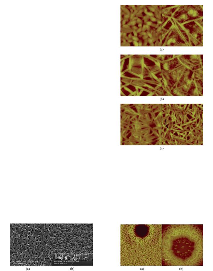
microstructure. In polymers, however, the elastic modulus can be strongly structure sensitive.16 Due to its similar chemical structure to the well-known crystalline polymer polyethylene (PE), the PVDF and P(VDF–TrFE) can be crystallized, and the resulting structure should be considered as semi-crystalline or a mixture of two phases, consisting of small crystallites and fully disordered amorphous material. Fig. 1 shows the typical crystalline morphology of P(VDF–TrFE) annealed at 140 C for an hour, obtained by scanning electron microscopy (SEM). The distinct elongated ellipsoidal particles can be clearly seen and are in good agreement with the literature.17–20
We used different substrates (bare Si, fluorinated self-assem- bled monolayer treated Si (FSAM-treated Si), and elastomeric polydimethylsiloxane (PDMS)) to see the effect of substrate on the crystallization behavior of P(VDF–TrFE) thin films. For the P(VDF–TrFE) thin films annealed at low temperatures (below the melting temperature of the copolymer, Tm ¼ 145–148 C), spherical crystalline grains were obtained even at room temperature and the grains increased in size as the annealing temperature increased from room temperature to 120 C (ESI, Fig. S1†). The crystallization behavior doesn’t exhibit any noticeable differences on different substrates at crystallization temperatures below 120 C.
When the film is annealed at 160 C, which is above the melting temperature, the small crystallites fuse into rods or fibers. Annealing at or near the Tm (e.g., 140 C) reveals different crystalline morphology depending on the substrate used. Lowenergy substrates such as FSAM-treated Si and PDMS enhance the crystallization rate, leading to rod/fiber shaped crystallites at the annealing temperature of 140 C, as shown in Fig. 2b and 2c. On the contrary, ellipsoidal crystalline grains were obtained on the high energy surface of bare Si at the same annealing temperature (Fig. 2a). Considering the sequential change in crystalline morphology of P(VDF–TrFE) from sphere to ellipsoid to rod/fiber as we increase the annealing temperature, the results shown in Fig. 2 indicate that the surface energy of substrate upon which the P(VDF–TrFE) film resides affects the crystallization kinetics; the lower the surface energy, the faster the crystallization. The increased chain mobility is likely to be responsible for the enhanced crystallization on low-energy surfaces, such as PDMS and FSAM-treated Si.
The increased chain mobility on low-energy surfaces leads to dewetting when a thin (< 100 nm) polymer film is annealed at
Fig. 2 Crystalline morphology of P(VDF–TrFE) thin films ( 90 nm) by atomic force microscopy on different substrates: (a) bare Si, (b) FSAMtreated Si, and (c) PDMS. Images on the left were for films annealed at 140 C, while those on the right were for films annealed at 160 C (scan size: 2 mm*2 mm for (a) and (b), 5 mm*5 mm for (c)).
high temperatures, due to a long-range van der Waals force.21,22 Fig. 3a shows the dewetted P(VDF–TrFE) film on the FSAMPDMS surface, annealed at 160 C for 1 h. An 90 nm thick film on FSAM-PDMS leaves 5 mm wide holes when annealed at elevated temperatures. Upon magnification, as shown in Fig. 3b, the receding circular rim leaves small dots arranged in circular
Fig. 1 Representative SEM images of 320 nm thick P(VDF–TrFE) film |
Fig. 3 Dewetted P(VDF–TrFE) film ( 90 nm) on FSAM-PDMS by |
on FSAM-treated Si wafer, annealed at 140 C for 1 h: (a) plane view and |
annealing at 160 C for 1 h. The scan area is 20 mm*20 mm for (a), and 10 |
(b) 15 tilted view. |
mm*10 mm for (b). |
|
|
This journal is ª The Royal Society of Chemistry 2010 |
Soft Matter, 2010, 6, 5802–5806 | 5803 |
Downloaded by Stanford University on 24 February 2013 |
Published on 20 September 2010 on http://pubs.rsc.org | doi:10.1039/C0SM00350F |
View Article Online
configuration, with fingers due to Rayleigh-Plateau or fingering instabilities.22
In the buckling-based moduli measurement of thin film samples, the films should be placed on a softer substrate, typically elastomer PDMS. Then the film/PDMS couple is compressed to induce mechanical buckling, where the applied compressive strain is usually small (below 3–5%). The excessive compressive strain usually leads to delamination of film from the substrate, unless special steps are taken to firmly adhere the film onto the substrate. Using the measured values of buckling wavelength and eqn (1) below, the modulus of the film can be determined.
|
|
|
|
|
l |
3 |
|
|
|
|
|
|
|
||
Ef ¼ |
3 EPDMS |
|
|
(1) |
|||
2 p h |
|||||||
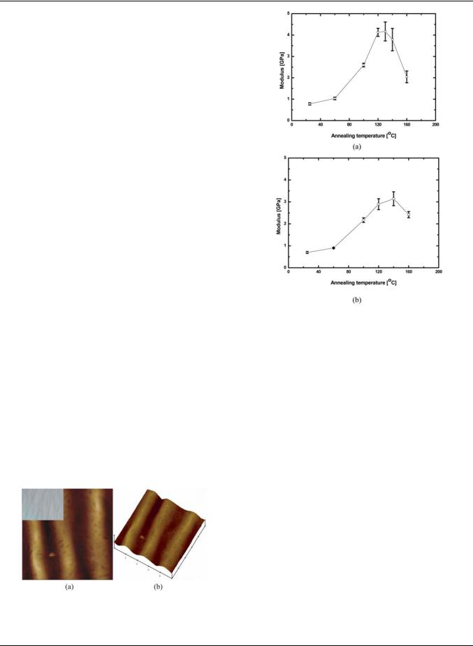
Here, E is the plane-strain modulus, l the buckling wavelength, h the film thickness, and subscripts f and PDMS denote film and substrate PDMS, respectively. Fig. 4 shows the typical images of buckled P(VDF–TrFE) film on PDMS. Note that the rod/fiber shaped crystalline morphology is visible in the 2- and 3-dimen- sional atomic force microscopy (AFM) images. The rod/fiberlike crystalline morphology can be seen to be retained and overlaid on the larger scale, buckled surface profile.
Fig. 5 shows the Young’s modulus of P(VDF–TrFE) films, annealed on FSAM-treated Si (Fig. 5a) and on PDMS (Fig. 5b), as a function of annealing temperature. The corresponding buckling wavelength data as a function of temperature are given in Fig. S2†. In Fig. S2†, some data points are missing, especially for thin films on PDMS. This is due to dewetting; the homogeneous films ruptured into discontinuous ones, which made it impossible to implement the buckling experiments. The moduli, shown in Fig. 5a and 5b, were determined, by eqn (1), from the slope of linear fit to wavelength vs. film thickness plot for each temperature. Note further that for thin films in Fig. S2†, the buckling wavelength seems almost constant regardless of annealing temperature, which is not in fact the case. This is due to the large difference in scale between the y-axis in those plots and the absolute values of buckling wavelength for such thin films.
Interestingly, the modulus value shows a peak at/around the annealing temperature of 120–140 C. Then, it decreases as we further increase the annealing temperature. As shown in Fig. 2 and Fig. S1†, the film microstructure depends strongly on the
Fig. 4 Optical and atomic force microscopy images of buckled 90 nm thick P(VDF–TrFE) film, annealed at 160 C for 1 h. (a) 2-Dimensional view with OM image as an inset, (b) perspective view of buckled surface of film.
Fig. 5 Buckling wavelengths and Young’s modulus of P(VDF–TrFE) thin films, prepared and annealed on FSAM-treated Si substrate (a) and on PDMS (b).
annealing temperature. Therefore, the change in modulus can be related to the difference in film microstructure. At annealing temperatures below 120–140 C, the spherical crystallites are formed in an amorphous matrix and they grow in size as the annealing temperature increases, which results in increase in modulus. There are two mechanisms for the effect of crystallinity on the mechanical modulus of a polymer.23 Firstly, crystallites can act as a kind of physical crosslinkers by tying segments of many polymer molecules together. Secondly, the crystallites have very high modulus compared to amorphous part, so they behave as rigid fillers in an amorphous matrix. These mechanisms explain the increase in P(VDF–TrFE) modulus in the annealing temperature range from room temperature to 120 C. The same arguments can be applied to the modulus decrease at high annealing temperatures. At high enough annealing temperatures, the ellipsoidal crystallites merge into rod/fiber geometry. This drastic change in crystallite morphology leads to sharp decrease in the crystallinity of the film, as confirmed by X-ray diffraction (XRD).20,24,25 According to XRD analysis of the P(VDF–TrFE) films annealed at different temperatures, the % crystallinity shows a maximum at/around 140 C, which is slightly lower than the melting temperature. Therefore, the change in modulus agrees very well with that of the % crystallinity of the films (also refer to Fig. S3 and S4†). This microstructure-dependent modulus confirms again the common belief in materials science that, for polymers as well as metals, better mechanical properties can be obtained with fine-grained microstructures.
5804 | Soft Matter, 2010, 6, 5802–5806 |
This journal is ª The Royal Society of Chemistry 2010 |

Downloaded by Stanford University on 24 February 2013 |
Published on 20 September 2010 on http://pubs.rsc.org | doi:10.1039/C0SM00350F |
|
|
|
|
|
View Article Online |
||
When the P(VDF–TrFE) film is spun and annealed on FSAM- |
annealed one. Further increase in crystallization temperature |
|
|||||
treated Si surface, it should be transferred onto elastomeric |
leads to a decrease in the modulus, which agrees well with |
||||||
PDMS to implement the buckling experiments. On the other |
decrease in crystallinity in the film annealed above the Tm. The |
||||||
hand, the sample can be directly used for the buckling experiment |
measured modulus of a ferroelectric P(VDF–TrFE) thin film can |
||||||
if the film is prepared on PDMS substrate from the beginning. |
be a great help in the design and fabrication of functional devices |
||||||
Fig. 5b shows the resulting moduli for P(VDF–TrFE) films |
using the polymer as an active component, such as in flexible or |
||||||
prepared and annealed directly on PDMS. The similar results to |
even stretchable nonvolatile memories and piezoelectric energy |
||||||
the FSAM-treated Si substrate, i.e., the maximum modulus at/ |
harvesting devices. |
||||||
around 120–140 C and then decrease in modulus at higher |
|
|
|||||
annealing temperatures, is obtained. But the absolute value of |
Experimental |
||||||
modulus is slightly smaller than that of the FSAM-treated Si |
|||||||
|
|
||||||
case, especially at temperatures of 120–140 C. Note that the |
Materials |
||||||
mechanical |
modulus of |
the PDMS substrate used in these |
P(VDF–TrFE), 70/30 mol%, was purchased from Solvay, and |
||||
experiments was separately measured by the micro-tensile test |
|||||||
dissolved in methylethylketone as a solvent. The solution |
|||||||
(Fig. S5†), and shows an 3 increase of modulus in the high- |
|||||||
concentration and spin speed were varied to obtain films with |
|||||||
temperature annealed PDMS, compared to the usual 60 C- |
different thicknesses, ranging from 30 nm to 1 mm. Si wafers |
||||||
cured ones ( |
|
4.5 MPa vs. |
|
1.5 MPa for PDMS substrates cured |
|||
|
|
|
were kindly supplied by LG Siltron, Co., Ltd (Korea) and |
||||
at 160 C and 60 C, respectively). To rule out the possible |
cleaned in acetone, isopropyl alcohol, and de-ionized water for |
||||||
adverse effect of PDMS, we used PDMS substrates that were |
|||||||
5 min in an ultrasonic bath, and then dried in an N2 stream. For |
|||||||
cured at 160 C for 2 h for the experiments and used the pertinent |
|||||||
modulus value of PDMS in calculating film modulus using |
FSAM-treated Si surface, the cleaned Si substrate was vacuum- |
||||||
deposited with a drop of trideca-fluoro-1,1,2,2-tetrahydrooctyl- |
|||||||
eqn (1). Although these approaches reduces the uncertainties in |
|||||||
trichlorosilane inside a dessicator. The FSAM-treatment of Si |
|||||||
the buckling experiments of P(VDF–TrFE) films on PDMS, they |
|||||||
surface was optimized (Fig. S6†), in terms of water contact angle |
|||||||
cannot completely remove other adverse effects. For example, |
|||||||
and surface smoothness. For the FSAM-treatment of PDMS, the |
|||||||
the unreacted oligomeric PDMS molecules26 can possibly diffuse |
|||||||
and mix with overlying film material, thereby affecting accurate |
cured slab of PDMS was briefly exposed to UV/ozone to make its |
||||||
|
|
||||||
determination of modulus of the film material. Or, the recovered |
surface have silanol (Si–OH) functionality, it then underwent the |
|
same vacuum deposition process as the Si substrate. The elas- |
||
PDMS oligomers could form a layer at the interface with the film |
||
tomer PDMS (Sylgard 184, Dow) was prepared by mixing the |
||
and may affect interfacial adhesion or sliding between the film |
||
base resin and the curing agent in a 10 : 1 ratio, which was |
||
and the PDMS substrate. |
||
degassed and cured at 60 C for >4 h. |
||
|
3. Conclusions
In summary, we have investigated crystallization behavior of ferroelectric P(VDF–TrFE) copolymer thin films on various substrates, as a function of crystallization temperature. At low crystallization temperatures, there was no noticeable difference in crystallization behavior among substrates used. At temperatures around the melting temperature of the polymer, the lowerenergy surfaces such as FSAM-treated Si and PDMS show enhanced crystallization behavior, due to the increased chain mobility on those surfaces. Upon further increase in crystallization temperature above Tm, thin (< 100 nm) films on those low-energy surfaces dewet whereas the film shows stable crystallization into rod/fiber form on the bare Si surface. The dewetted holes on the low-energy surface have small nanoscale dots in them, and show Rayleigh-Plateau or fingering instabilities around the receding rims. The dewetting phenomenon may be useful to pattern the ferroelectric polymers in the nanoscale, with proper steps to control/guide the dewetting (structured PDMS substrate, for example).
The Young’s modulus of thin P(VDF–TrFE) films has been measured by the buckling experiments. The drastically different microstructures of crystallized P(VDF–TrFE) films at different temperatures are found to be closely related to the mechanical modulus. The maximum in the modulus approximately corresponds to the maximum % crystallinity of the film. The modulus can be varied almost over an order of magnitude, from 0.4 GPa for a room temperature dried film to 4 GPa for a 120–140 C
Film crystallization
The P(VDF–TrFE) films that were spun on to the substrates (bare Si, FSAM-treated Si, and PDMS) were vacuum dried at room temperature, or annealed at elevated temperatures in a convection oven for 1 h. The crystallized microstructures of the films were investigated by atomic force microscopy (AFM, Veeco D3100), which was used to measure the film thickness as well, and scanning electron microscopy (FEI 3000, ZEOL).
Buckling experiment
The crystallized films on FSAM-treated Si substrates were instantaneously picked-up onto flat PDMS slabs,27 while the films prepared and annealed on PDMS were directly used for the buckling experiments. The films on PDMS showed local buckling due to thermally-induced buckling when cooled down from high temperature to room temperature. But, most of the film surface remained flat. The buckling wavelengths, measured both on thermally-buckled spots and on flat area wrinkled by external compression, showed similar values. The film/PDMS sample was loaded onto a home-made compression stage and a small compression applied, typically smaller than 3%, and was observed under the optical microscope (OM, Olympus BX60) equipped with a digital camera. The buckling wavelength was determined from the acquired OM images, by measuring the horizontal distance of many waves (>10 waves) and dividing it by
This journal is ª The Royal Society of Chemistry 2010 |
Soft Matter, 2010, 6, 5802–5806 | 5805 |

Downloaded by Stanford University on 24 February 2013 |
Published on 20 September 2010 on http://pubs.rsc.org | doi:10.1039/C0SM00350F |
|
|
|
|
View Article Online |
||||
the number of waves within. The wavelength values measured by |
14 |
D.-Y. Khang, J. A. Rogers and H. H. Lee, Adv. Funct. Mater., 2009, |
|
|||||
AFM compared well with those from OM measurements. |
|
19, 1526. |
|
|
|
|
||
15 |
S.-W. Hahm, H.-S. Hwang, D. Kim and D.-Y. Khang, Electron. |
|||||||
|
|
|||||||
Acknowledgements |
|
Mater. Lett., 2009, 5, 157. |
|
|
|
|
||
16 |
D. T. Grubb, in Structure and Properties of Polymers, ed. E. L. |
|||||||
|
|
|||||||
This work was supported by the WCU (World Class University) |
|
Thomas, VCH Publishers, New York, 1993, ch. 7, pp. 301–356. |
||||||
17 |
X. Chen, H. Yamada, T. Horiuchi and K. Matsushige, Jpn. J. Appl. |
|||||||
program through the National Research Foundation of Korea |
||||||||
|
Phys., 1998, 37, 3834; T. Fukuma, K. Kobayashi, T. Horiuchi, |
|||||||
funded by the Ministry of Education, Science and Technology |
|
|||||||
|
H. Yamada and K. Matsuchige, Jpn. J. Appl. Phys., 2000, 39, 3830; |
|||||||
(R32-20031). |
|
K. Kimura, K. Kobayashi, H. Yamada, T. Horiuchi, K. Ishida and |
||||||
|
|
|
K. Matsushige, Appl. Surf. Sci., 2006, 252, 5489. |
|
|
|
||
Notes and references |
18 |
G. Zhu and J. Li, Ferroelectrics, 2004, 300, 95. |
|
|
|
|||
|
|
19 |
W. Li, Y. Zhu, D. Hua, P. Wang, X. Chen and J. Shen, Appl. Surf. |
|||||
1 |
T. T. Wang, J. M. Herbert, and A. M. Glass, The Applications of |
|
Sci., 2008, 254, 7321. |
|
|
|
|
|
|
Ferroelectric Polymers. Chapman & Hall, New York, 1998. |
20 |
S.-W. Jung, S.-M. Yoon, S. Y. Kang and B.-G. Yu, Integr. |
|||||
2 |
R. C. G. Naber, C. Tanase, P. W. M. Blom, G. H. Gelinck, |
|
Ferroelectr., 2008, 100, 198. |
|
|
|
|
|
|
A. W. Marsman, F. J. Touwslager, S. Setayesh and D. M. de |
21 |
G. Reiter, Phys. Rev. Lett., 1992, 68, 75. |
|
|
|
||
|
Leeuw, Nat. Mater., 2005, 4, 243. |
22 |
G. Reiter, Langmuir, 1993, 9, 1344. |
|
|
|
||
3 |
K. H. Lee, G. Lee, K. Lee, M. S. Oh, S. Im and S.-M. Yoon, Adv. |
23 |
L. E. Nielson and R. F. Landel, Mechanical properties of polymers and |
|||||
|
Mater., 2009, 21, 4287. |
|
composites. Marcel Dekker, New York, 1994. |
|
|
|
||
4 |
C. Chang, V. H. Tran, J. Wang, Y.-K. Fuh and L. Lin, Nano Lett., |
24 |
Z.-G. Zeng, G.-D. Zhu, L. Zhang and X.-J. Yan, Chin. J. Polym. Sci., |
|||||
|
2010, 10, 726. |
|
2009, 27, 479. |
|
|
|
|
|
5 |
H. Ohigashi, K. Koga, M. Suzuki, T. Nakanishi, K. Kimura and |
25 |
Y. Tajitsu, H. Ogura, A. Chiba and T. Furukawa, Jpn. J. Appl. Phys., |
|||||
|
N. Hashimoto, Ferroelectrics, 1984, 60, 263. |
|
1987, 26, 554. |
|
|
|
|
|
6 |
J. F. Legrand, Ferroelectrics, 1989, 91, 303. |
26 |
H. Hillborg and U. W. Gedde, Polymer, 1998, 39, 1991; H. Hillborg |
|||||
7 |
J. K. Kruger, M. Prechtl, J. C. Wittmann, S. Meyer, J. F. Legrand and |
|
and U. W. Gedde, IEEE Trans. Dielectr. Electr. Insul., 1999, 6, 703; |
|||||
|
G. D’asseza, J. Polym. Sci., Part B: Polym. Phys., 1993, 31, 505. |
|
I. Bohm, A. Lampert, M. Buck, F. Eisert and M. Grunze, Appl. |
|||||
8 |
Q. M. Zhang, V. Bharti and X. Zhao, Science, 1998, 280, 2101. |
|
Surf. Sci., 1999, 141, 237; D. |
J. Graham, D. |
D. |
Price and |
||
9 |
K. Omote, H. Ohigashi and K. Koga, J. Appl. Phys., 1997, 81, 2760. |
|
B. D. Ratner, Langmuir, 2002, 18, 1518; K. Glasmastar, J. Gold, |
|||||
10 |
C. Huang, F. Xia, H. Li, Q. M. Zhang, F. Bauer and Z.-Y. Cheng, |
|
A.-S. Andersson, D. S. Sutherland and B. Kasemo, Langmuir, 2003, |
|||||
|
IEEE Trans. Dielectr. Electr. Insul., 2004, 11, 299. |
|
19, 5475; R. B. A. Sharpe, |
D. Burdinski, C. |
v. |
d. Marel, |
||
11 |
C. M. Stafford, C. Harrison, K. L. Beers, A. Karim, E. J. Amis, |
|
J. A. J. Jansen, J. Huskens, H. J. W. Zandvliet, D. N. Reinhoudt |
|||||
|
M. R. Vanlandingham, H. C. Kim, W. Volksen, R. D. Miller and |
|
and B. Poelsema, Langmuir, |
2006, 22, 5945; |
C. |
Thibault, |
||
|
E. E. Simonyi, Nat. Mater., 2004, 3, 545. |
|
C. Severac, A.-F. Mingotaud, C. Vieu and M. Mauzac, Langmuir, |
|||||
12 |
E. P. Chan and A. J. Crosby, in Polymer Thin Films, ed. O. K. C. Tsui |
|
2007, 23, 10706. |
|
|
|
|
|
|
and T. P. Russel, World Scientific, Singapore, 2008, ch. 6, pp.141–161. |
27 |
M. A. Meitl, Z.-T. Zhu, V. Kumar, K. J. Lee, X. Feng, Y. Y. Huang, |
|||||
13 |
D. H. Tahk, H. H. Lee and D.-Y. Khang, Macromolecules, 2009, 42, 7079. |
|
I. Adesida, R. G. Nuzzo and J. A. Rogers, Nat. Mater., 2006, 5, 33. |
|||||
5806 | Soft Matter, 2010, 6, 5802–5806 |
This journal is ª The Royal Society of Chemistry 2010 |