

Статьи на перевод PVDF_P(VDF-TrFE) / Память на с-э полимерах
.pdfwww.advmat.de
www.MaterialsViews.com
Flexible Non-Volatile Ferroelectric Polymer Memory with Gate-Controlled Multilevel Operation
Sun Kak Hwang, Insung Bae, Richard Hahnkee Kim, and Cheolmin Park*
Ferroelectric-gate field-effect transistors (Fe-FETs) employing ferroelectric layers as gate insulators have received attention due to their benefits, including a non-destructive readout capability, scalable feature size of 4F2, and low operating voltages.[1,2] In an Fe-FET, the polarization state of the ferroelectric layer is set by the polarity of the program/erase gate voltage, which controls accumulation or depletion of carriers in the semiconducting channel between the source and drain electrode.[2,3] Due to the potential advantages of ferroelectric polymers including their low cost, easy solution processes fabrication, and mechanical pliability (which allows for the production of flexible, foldable, and stretchable devices), great efforts have been devoted to improve the properties of Fe-FETs using ferroelectric polymers such as poly(vinylidene fluoride) (PVDF) and its copolymers with trifluoroethylene (PVDF-TrFE). In particular, efforts have been made to improve their non-destructive readout capa- bility,[3,4–6] flexibility,[6,7] printing capability,[8] endurance,[3,9] long data retention,[3,4,6] short program pulse width,[3] large ON/OFF ratio,[3,4,8,9] and operating voltage,[10] as well as material design including electrodes,[3] ferroelectric and insulating layers,[4,6,10] and organic semiconducting active layers.[3,4–6,8,11–21]
One of the most pressing issues yet to be significantly addressed is the fabrication of high-density Fe-FETs. Highdensity memories can be realized by continuous scale-down of individual cell dimensions as well as 3D stacking of planar arrays of memory elements.[22] However, these two approaches require elaborate and expensive micro/nanofabrication processes which are often harmful to polymers, as well as very careful selection of materials appropriate for the multistacking solution process. An alternative solution is a memory cell with multilevel data storage capability.
A variety of multilevel memory cells (MLCs) have recently been fabricated based on either flash or resistive switching operation.[23–28] The key materials of the majority of MLCs are inorganic, such as Au nanoparticles,[23] Ni nanocrystals,[24] and ZrO2[25] and cobalt oxide nanowires.[26] Only a few organic MLCs have been fabricated, and these made use of small molecules[27] and solution-processed graphene oxide.[28] Multilevel operation of memory cells containing mechanically stiff inorganic
S. K. Hwang, I. Bae, R. H. Kim, Prof. C. Park,
Department of Materials Science and Engineering
Yonsei University
Seoul, 120-749, Republic of Korea
E-mail: cmpark@yonsei.ac.kr
DOI: 10.1002/adma.201201831
semiconducting channels was also achieved using ferroelectrics under principles of continuous ferroelectric domain switching of PbZrT1–xO3 (PZT), as well as periodic thickness variation of a PVDF-TrFE layer by nanoimprinting lithography.[29,30] However, they frequently suffer from poor data reliability, and in particular, unstable switching endurance.
In this paper, we demonstrate a highly reliable and mechanically flexible MLC Fe-FET with a thin PVDF-TrFE insulator. Our device is based on multileveled non-volatile drain current states of a polymeric semiconductor precisely controlled by a ferroelectric insulator. Various remnant polarization states which arise from distributed domain polarization of the ferroelectric layer as a function of the applied gate voltage in turn dictate the interstate levels of the source-drain current (IDS), giving rise to a highly reliable 4-level MLC Fe-FET. Each level of the device exhibited excellent data retention and endurance of more than 105 s and 102 cycles, respectively. Furthermore, our gate-controlled multilevel Fe-FETs with poly(3-hexyl thiophene) (P3HT) active channels are mechanically flexible with characteristic multilevels even after more than 1000 bending cycles, with a bending radius of 5.8 mm.
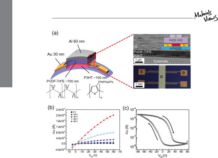
An Fe-FET memory device with a top-gate bottom-contact (TGBC) structure consisting of an Au source-drain (S/D) elec- trode/P3HT/PVDF-TrFE/Al gate electrode was constructed on either a Si wafer or a flexible polymer substrate as schematically illustrated in Figure 1a. The TGBC structure is suitable for high-density circuit design and is also effective for facile accumulation of charge carriers in channels upon non-volatile dipole switching of PVDF-TrFE by a gate voltage (VG).[31] A 100 nm-thick P3HT layer was directly spin-coated from solution in 1, 2-dichlorobenzene onto the patterned Au S/D electrodes. Subsequently, a 700 nm-thick PVDF-TrFE layer (60 mg/ml in methyl ethyl ketone (MEK) solvent) was spin-coated onto the P3HT layer, followed by thermal evaporation of the Al gate electrodes. To isolate between two cells as well as to make the Au S/D electrode accessible to contact probes, both the P3HT and PVDF-TrFE layers in the regions outside the areas covered by the top Al electrodes were etched by oxygen plasma using reactive ion etching (RIE), producing an Fe-FET device. The Fe-FET device was visualized using scanning electron microscopy (SEM) and optical microscopy, as shown in Figure 1a.
The Fe-FET with the P3HT channel layer exhibited p-type output characteristics in the IDS versus source-drain voltage (VDS) curve and the transfer curve (at a VDS of –5 V), which showed current hysteresis as a function of VG arising from the ferroelectric polarization switching of PVDF-TrFE, as shown in Figure 1b,c. The hysteresis curve was saturated when a VG above ±80 V was applied. After the device was turned on, there was a rapid increase of the IDS with a negative bias in VG due
COMMUNICATION
Adv. Mater. 2012, |
© 2012 WILEY-VCH Verlag GmbH & Co. KGaA, Weinheim |
wileyonlinelibrary.com 1 |
DOI: 10.1002/adma.201201831 |
|
|
www.advmat.de
www.MaterialsViews.com
COMMUNICATION
Figure 1. a) Schematic of the TGBC Fe-FET memory device with a P3HT channel and ferroelectric PVDF-TrFE insulator. SEM image (top) and photograph (bottom) showing cross-sectional and plan views of the Fe-FET, respectively. b) I–V output plots of the Fe-FET device. c) IDS–VG transfer curve of the device demonstrating characteristic current hysteresis arising from the non-volatile ferroelectric polarization of the PVDF-TrFE layer.
to accumulation of excess holes in the P3HT layer. When the VG returned to zero, the IDS still remained saturated due to the non-volatile H–F dipoles, with the fluorine atoms pointing to the P3HT layer. The subsequent application of a positive VG on the device gradually switched the H–F dipoles, leading to a decrease in the IDS. The non-volatility of the polarization caused the current to remain constant after the removal of the positive voltage, as shown in Figure 1c. We optimized the thickness of PVDF-TrFE to maximize the ON/OFF current ratio and to ensure a clear margin between the interstate levels for a multilevel device (Supporting Information, Figure S1). The best ON/OFF ratio (>103) was observed in the Fe-FET with a PVDFTrFE layer prepared from a 60 mg/ml solution (≈700 nm in Figure 1a).
Multilevel data storage of the IDS as controlled by continuous ferroelectric domain switching of a PVDF-TrFE insulator was examined as a function of gate voltage and the results are shown in Figure 2a. First, the OFF state (erase state) in an Fe-FET was
set up with a VG of +80 V in DC sweep mode. The IDS values measured at VG = 0 V after various DC sweep gate voltage steps
clearly indicated the presence of non-volatile current states with an almost continuous increase when the program gate voltage sweep was above –10 V, as shown in Figure 2a. At a high gatevoltage sweep, above –70 V, the IDS at VG = 0 V did not vary significantly due to saturation of the channel. In the gate voltage
sweep regions from –10 to –70 V, a portion of the non-vola- tile H–F dipoles (with the fluorine atoms pointing to P3HT) increased with the increasing gate voltage sweep due to pseudocontinuous ferroelectric switching of the PVDF-TrFE insulator. In this case, three distinct processes, the interbond process, intermolecular expansion of chain rotation, and interlamellar expansion of polarization reversal, occur simultaneously.[32] The continuous ferroelectric switching is readily expected since more than 107 needle-like PVDF-TrFE crystalline domains with dimensions of approximately 200 nm × 40 nm developed in the current device channel area.[1] The results imply that multilevel operation of a cell is achievable as long as the programming gate voltage sweep is precisely controlled with a sufficient reading margin of the IDS at VG = 0 V between two levels. The Fe-FET also exhibited multilevel erasing behavior similar to that observed for programming (Figure S2).
To demonstrate a four-level Fe-FET, we chose two interstates (IRS) with program voltages at –30 and –50 V, in addition to complete erase and saturated program states (ERS and PGM) at +80 and –80 V, respectively. After complete erase at VG = +80 V, the lowest current state OFF state was set as the ERS, as shown in Figure 2b. The subsequent gate voltage sweep at
±30 V resulted in a IDS hysteresis curve with the second level state, IRS-1. Additional sweep at ±50 V again gave rise to the third level non-volatile IDS state, IRS-2. Finally, a full sweep
2 wileyonlinelibrary.com |
© 2012 WILEY-VCH Verlag GmbH & Co. KGaA, Weinheim |
Adv. Mater. 2012, |
|
|
DOI: 10.1002/adma.201201831 |

www.advmat.de
www.MaterialsViews.com
COMMUNICATION
Figure 2. a) Non-volatile IDS values obtained at a read voltage (VG = 0 V) after various program VG values ranging from –5 to –80 V in the DC sweep mode. The four distinct IDS values at appropriate program voltages highlighted in (a) were used for the four-level Fe-FET. b) The multilevel IDS–VG transfer curves of an Fe-FET after various program VG values. The schematic in the inset shows non-volatile IDS levels controlled by the ferroelectric polarization at different program gate voltages.
at ±80 V developed a saturated IDS hysteresis curve with the fourth level state, PGM, as shown in Figure 2b. The schematics in Figure 2b illustrate non-volatile IDS levels controlled by ferroelectric polarization switching of a PVDF-TrFE insulator at different program gate voltages. It should be, however, noted that the operating voltage of our multilevel device is still high due to the large coercive field of PVDF-TrFE for ferroelectric switching, compared with the recent state-of-the art flash type organic memory[33] and thus further effort should be made to reduce the operating voltage by elaborate control of both microstructure of the ferroelectric layer and device architecture.[10]
The memory device reliability of our four-level Fe-FET was examined by both time dependent data retention and multiple data writing/erasing endurance. Data retention was evaluated by independently measuring four non-volatile IDS values set by
Figure 3. a) The time-dependent retention characteristics and b) multiple write/erase endurance cycles of multilevel IDS values established in an Fe-FET. The insets in (a) and (b) show the test sequence applied in the DC sweep mode for the multilevel retention and endurance measurements, respectively. For clarity, one cycle out of every 4 cycles is represented in (b).
different gate voltage sweeps at VG = 0 V with a constant VDS of –5 V, as schematically illustrated in the inset of Figure 3a. Figure 3a shows highly reliable data retention of all four states for up to approximately 105 s. Our multilevel retention results are very promising when one considers that most inorganic FeFETs suffer from poor data retention due to a severe depolarization field.[34,35]
For multiple data write/erase endurance measurements, we consecutively read four-level non-volatile IDS values with the programmed endurance cycle. The sequence used was erase/read/ program-1/read/program-2/read/program-3/read with four corresponding DC program gate sweeps of +80–0 V, –30–0 V, –50–0 V, and –80–0 V, as depicted in the inset of Figure 3b. Very consistent and reliable rewritable four-level cycles were observed over 100 cycles, as shown in Figure 3b. As predicted previously, the degree of ferroelectric polymer domain switching was precisely controlled and remained unchanged when a constant set gate voltage was repeatedly applied. The highly reliable data retention and endurance performance of our four-level Fe-FET memory is indeed notable, considering that most multilevel organic memories demonstrate long data retention but often exhibit unstable multilevel switching endurance. This is mainly due to the degradation of the tunneling layer or conducting filament under repeated program/erase
Adv. Mater. 2012, |
© 2012 WILEY-VCH Verlag GmbH & Co. KGaA, Weinheim |
wileyonlinelibrary.com 3 |
DOI: 10.1002/adma.201201831 |
|
|
COMMUNICATION
www.advmat.de
www.MaterialsViews.com
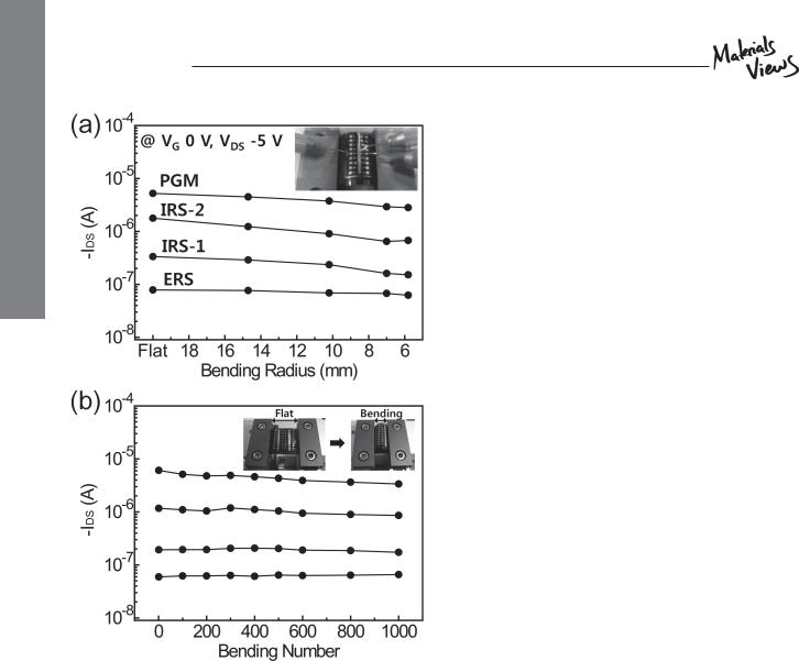
Figure 4. The multilevel IDS values of a flexible Fe-FET memory: a) as a function of the bending radius, and b) as a function of the number of bending cycles under a bending radius of 5.8 mm. The inset in (a) exhibits a photograph of a flexible Fe-FET obtained under bending. The photographs in the inset of (b) show arrays of Fe-FETs in bent and unbent states.
cycles.[23,24,27] Our Fe-FET memory is beneficial because of the non-destructive device operation with FET architecture based on polarization switching, which is electrically much more stable than conduction switching. As a result, our multilevel FeFETs demonstrated good cell-to-cell uniformity in the IDS distribution at each level (Supporting information, S3).
Flexible multilevel Fe-FETs fabricated on polyimide substrates also showed reliable four-level non-volatile I–V characteristics similar to those on SiO2 (Supporting information, S4). We investigated the bending stability of our device in which four independent IDS values set up with corresponding gate voltage sweeps were monitored as a function of the bending radius, as shown in Figure 4a. The IDS values of the four states were similar, without any notable current fluctuation even under a bending radius of 5.8 mm, as shown in Figure 4a (Supporting information, S4). We further examined the memory stability of our Fe-FET as a function of the number of bending cycles. The
device exhibited very stable four-level memory characteristics after more than 1000 bending cycles using a radius of 5.8 mm, as shown in Figure 4b. Our four-level Fe-FET on a flexible substrate also demonstrated reliable long term data retention and multiple write/erase endurance under severe bending at a radius of 5.8 mm (Supporting information, S5). Considering that Curie temperature of the PVDF-TrFE is approximately 80 °C, our results clearly suggest that 1 T memory based on ferroelectric polymer can be one of the most-promising candidates for emerging flexible, high-density, non-volatile memories with reasonable thermal margin.
In summary, we have demonstrated a flexible non-volatile Fe-FET memory with multilevel switching behavior by precisely controlling the degree of remnant polarization of a ferroelectric PVDF-TrFE gate insulator which was dependent on the applied gate voltage. Four levels of discrete non-volatile source-drain currents were readily achieved with the application of an appropriate programming/reading gate voltage, and the memory exhibited an excellent data retention of more than 105 s and a notable multiple write/erase endurance of 102 cycles. Furthermore, our multilevel Fe-FET fabricated on a polymer substrate provided mechanical flexibility in which the characteristic 4-level reliable switching was also realized with more than 1000 bending cycles at a bending radius of 5.8 mm. Our results offer a novel design strategy for low-cost high-density organic memory and are conveniently adoptable for various flexible and foldable organic electronic devices.
Experimental Section
Materials and Film Preparation: PVDF-TrFE with 25 wt% TrFE was purchased from MSI Sensors. P3HT (Mw = 180 000 g mol−1 with 98.5% head-to-tail regioregularity) was purchased from Sigma–Aldrich, Korea. All of the organic solvents including methyl ethyl ketone (MEK) and 1,2-dichlorobenzne (DCB) were purchased from Sigma–Aldrich, Korea. A P3HT solution in DCB (1 wt%) was spin-coated at 2000 rpm for 70 s on either a SiO2 (500 nm) or polyimide substrate with patterned Au S/D electrodes. A PVDF-TrFE solution in MEK (40, 60, and 80 mg/ml) was spin-coated at 1500 rpm for 60 s on a P3HT layer. The spin-coated films were dried under vacuum for 2 h at 60 °C.
Device Fabrication and Characterization: SiO2 substrates were cleaned in an ultrasonic bath with acetone and ethanol for 1 h each while the polyimide substrates used to make the flexible device were cleaned only in ethanol for 2 h. Firstly, arrays of 30 nm-thick Au S/D electrodes were thermally evaporated on a substrate with a patterned shadow mask under a vacuum of 10−6 Torr (SNTEK MEP5000). Subsequently, an approximately 100 nm-thick P3HT layer was spin-coated, followed by thin-film formation of a ferroelectric PVDF-TrFE insulator. The PVDFTrFE solution in MEK did not affect the underlying P3HT layer. After thermal treatment at 60 °C for 1 h to remove the residual solvents in both the P3HT and PVDF-TrFE layers, 60 nm-thick top gate Al electrodes were deposited by thermal evaporation under a vacuum of 10−6 Torr with a patterned shadow mask aligned with respect to the S/D electrodes previously formed. In order to make the Au S/D electrode accessible with contact probe tips, the devices were further treated with oxygen plasma (100 W for 200 s, 10−3 Torr, 40 sccm) generated by reactive ion etching (RIE) (Femto VITA-4E). Arrays of Al gate electrodes were used as RIE blocking masks, giving rise to top-gate-bottom-contact Fe-FET memories with S/D electrodes open to the air, as illustrated in the schematic in Figure 1a. The electrical characteristics were measured by semiconductor systems (E5270B, Agilent Technologies) under ambient conditions. Fieldemission scanning electron microscope (FESEM) images were obtained
4 wileyonlinelibrary.com |
© 2012 WILEY-VCH Verlag GmbH & Co. KGaA, Weinheim |
Adv. Mater. 2012, |
|
|
DOI: 10.1002/adma.201201831 |

www.MaterialsViews.com
using a LEO 1550 VP instrument with an acceleration voltage of 15 kV without any metal deposition. An optical microscope (OM) was used to visualize the Fe-FET devices (Olympus BX 51M).
Supporting Information
Supporting Information is available from the Wiley Online Library or from the author.
Acknowledgements
This research was supported by the Converging Research Center Program through the Ministry of Education, Science, and Technology (No. 2011K000631). This research was also supported by the Second Stage of the Brain Korea 21 Project in 2006 and a Korea Science and Engineering Foundation (KOSEF) grant funded by the Ministry of Science and Technology (MEST), Republic of Korea (No. R11-2007-050-03001-0).
Received: May 7, 2012
Published online:
[1]Y. J. Park, I.-S. Bae, S. J. Kang, J. Chang, C. Park, IEEE Trans. Dielectrics Electrical Insulation 2010, 17, 1135.
[2]X. Zhang, K. Miyaji, M. Takahashi, K. Takeuchi, S. Sakai, in
3rd IEEE Int. Memory Workshop (IMW), 2011, IEEE, Piscataway NJ
2011, 155, DOI: 10.1109/IMW.2011.5873233.
[3]R. C. G. Naber, C. Tanase, P. W. M. Bloom, G. H. Gelinck,
A.W. Marsman, F. J. Touwslager, S. Setayesh, D. M. De Leeuw, Nat. Mater. 2005, 4, 243.
[4]S. J. Kang, I. Bae, Y. J. Park, T. H. Park, J. Sung, S. C. Yoon, K. H. Kim,
D.H. Choi, C. Park, Adv. Funct. Mater. 2009, 19, 1609.
[5]R. C. G. Naber, B. De Boer, P. W. M. Blom, D. M. De Leeuw, Appl. Phys. Lett. 2005, 87, 203509.
[6] |
S. J. Kang, |
Y. J. Park, I. Bae, K. J. Kim, H.-C. Kim, S. Bauer, |
|
E. L. Thomas, C. Park, Adv. Funct. Mater. 2009, 19, 2812. |
|
[7] |
G.-G. Lee, |
E. Tokumitsu, S.-M. Yoon, Y. Fujisaki, J.-W. Yoon, |
H.Ishiwara, Appl. Phys. Lett. 2011, 99, 012901.
[8]T. Sekitani, K. Zaitsu, Y. Noguchi, K. Ishibe, M. Takamiya, T. Sakurai,
T.Someya, IEEE Trans. Electron Devices 2009, 56, 1027.
[9]K. Zaitsu, S. Lee, K. Ishibe, T. Sekitani, T. Someya, J. Appl. Phys. 2010, 107, 114506.
[10]S. J. Kang, I.-S. Bae, Y. J. Shin, Y. J. Park, J. Huh, S. M. Park,
H.C. Kim, C. Park, Nano Lett. 2011, 11, 138.
[11]R. C. G. Naber, M. Mulder, B. De Boer, P. W. M. Bloom,
D.M. De Leeuw, Adv. Mater. 2005, 17, 2692.
www.advmat.de
[12]W. Choi, S. H. Noh, D. K. Hwang, J.-M. Choi, S. Jang, E. Kim, S. Im,
Electrochem. Solid-State Lett. 2008, 11, H47.
[13]K. N. N. Unni, R. De Bettingnies, S. D. Seignon, J.-M. Nunzi, Appl. Phys. Lett. 2004, 85, 1823.
[14]C. A. Nguyen, S. G. Mhaisalkar, J. Ma, P. S. Lee, Org. Electron. 2008, 9, 1087.
[15]J. Chang, C. H. Shin, Y. J. Park, S. J. Kang, H. J. Jeong, K. J. Kim,
C.J. Hawker, T. P. Russell, D. Y. Ryu, C. Park, Org. Electron. 2009, 10, 849.
[16]S. H. Noh, W. Choi, M. S. Oh, D. K. Hwang, K. Lee, S. Im, S. Jang,
E.Kim, Appl. Phys. Lett. 2007, 90, 113509.
[17]L. Liao, H. J. Fan, B. Yan, Z. Zhang, L. L. Chen, B. S. Li, G. Z. Xing,
Z.X. Shen, T. Wu, X. W. Sun, J. Wang, T. Yu, ACS Nano, 2009, 3, 700.
[18]G. A. Salvatore, D. Bouvet, I. Stolitchnov, N. Setter, A. M. Ionescu, in Proc. 38th European Solid-State Device Research Conference (ESSDERC 2008), IEEE, PiscatawayNJ, 2008 162; DOI: 10.1109/ ESSDERC.2008.4681724.
[19]A. Gerber, M. Fitsilis, R. Waser, T. J. Reece, E. Rije, S. Ducharme,
H.J. Kohlstedt, J. Appl. Phys. 2010, 107, 124119.
[20]S.-M. Yoon, S.-H. Yang, S.-W. Jung, C.-W. Byun, S.-H. K. Park, C.-S. Hwang, G.-G. Lee, E. Tokumitsu, H. Ishiwara, Appl. Phys. Lett. 2010, 96, 232903.
[21]Y. Zheng, G.-X. Ni, C.-T. Toh, M.-G. Zeng, S.-T. Chen, K. Yao,
B.Ozyilmaz, Appl. Phys. Lett. 2009, 94, 163505.
[22]B. Cho, S. Song, Y. Ji, T. W. Kim, T. Lee, Adv. Funct. Mater. 2011, 21, 2806.
[23]J.-S. Lee, Y. Song, Y.-M, Kim, J.-H. Kwon, J. S. Sim, H. Shin, B.-H. Shon, Q. Jia, Adv. Mater. 2011, 23, 2064.
[24]J. G. Park, W. S. Nam, S. H. Seo, Y. G. Kim, Y. H. Oh, G. S. Lee,
U.G. Paik, Nano Lett. 2009, 9, 1713.
[25]M. Liu, Z. Abid, W. Wang, X. He, Q. Liu, W. Guan, Appl. Phys. Lett. 2009, 94, 233106.
[26] K. Nagashima, T. Yanagida, K. Oka, T. K. Taniguchi, J. Kim,
B.H. Park, Nano Lett. 2010, 10, 1359.
[27]B. C. Das, A. J. Pal, Org. Electron. 2008, 9, 39.
[28]C. Wu, F. Li, Y. Zhang, T. Guo, T. Chen, Appl. Phys. Lett. 2011, 99, 042108.
[29]A. K. Tripathi, A. J. J. M. Van Brremen, J. Shen, Q. Gao, M. G. Lvan,
K.Reimann, E. R. Meinders, G. H. Gelinck, Adv. Mater. 2011, 23, 4146.
[30]Y. Kaneko, Y. Nishitani, M. Ueda, E. Tokumitsu, E. Fujii, Appl. Phys. Lett. 2011, 99, 182902.
[31]T.J. Richards, H. Sirringhaus, J. Appl. Phys. 2007, 102, 094510.
[32]T. Furukawa, M. Date, M. Ohuchi, A. Chiba, Jpn. J. Appl. Phys. 1984, 56, 1481.
[33]M. Kaltenbrunner, P. Stadler, R. Schwodiauer, A. W. Hassel,
N.S. Sariciftci, S. Bauer, Adv. Mater. 2011, 23, 4892.
[34]T. P. Ma, J.-P. Han, IEEE Electron Device Lett. 2002, 23, 386.
[35]X. Pan, T. P. Ma, Appl. Phys. Lett. 2011, 99, 013505.
COMMUNICATION
Adv. Mater. 2012, |
© 2012 WILEY-VCH Verlag GmbH & Co. KGaA, Weinheim |
wileyonlinelibrary.com 5 |
DOI: 10.1002/adma.201201831 |
|
|