

Статьи на перевод PVDF_P(VDF-TrFE) / Ferroelectric P(VDF-TrFE) Ultrathin Film for SPM-Based Data Storage Devices
.pdfSolid State Phenomena Vols. 124-126 (2007) pp 303-306 Online available since 2007/Jun/15 at www.scientific.net © (2007) Trans Tech Publications, Switzerland doi:10.4028/www.scientific.net/SSP.124-126.303
Ferroelectric P(VDF/TrFE) Ultrathin Film for SPM-based Data Storage Devices
Jong Soon Lee1, Kap Jin Kim1,a and Arun Anand Prabu2
1Department of Advanced Polymer & Fiber Materials, College of Environment and Applied
Chemistry, Kyung Hee University, Yongin, 449-701, Korea
2Industrial Liaison Research Institute, Kyung Hee University, Yongin, 449-701, Korea
aCorresponding author: kjkim@khu.ac.kr
Keywords: Vinylidene fluoride-trifluoroethylene copolymer, data storage, SPM, electrical studies
Abstract. In this paper, the surface crystalline morphology and piezoelectricity of P(VDF/TrFE)(72/28) copolymer ultrathin films were studied using different scanning probe microscopy (SPM) techniques. Atomic force microscopy (AFM) was used to study the changes in their crystalline morphology with varying temperature conditions. From electric force microscopy (EFM) studies, the change in dipole moment vectors along the applied field direction and the resultant change in amplitude image for '1 or 0' state were monitored and used to 'write/erase and read' the data on the memory bit. These results indicate the possibility of using SPM-based high density data storage with these copolymer ultrathin films.
Introduction
In recent past, the principles of scanning probe microscopy (SPM) have been widely applied for data storage applications using polymeric ultrathin films. LG, Korea has demonstrated a low power SPM probe-based high density data storage system which uses a new read-write mechanism called “Thermo-piezoelectric method” in which the cantilever tip equipped with a heater is used for making an indentation (stands for a logical '1') on a PMMA film [1,2]. Erasing the data is performed by heating either entire plastic or its local region. Though this approach allows for reaching densities of hundreds Gbit per square inch, the main drawback is that writing data by this thermal method changes the polymer surface morphology and limits its usage to Write-Once-Read-Many (WORM) applications.
Replacing PMMA with ferroelectric polymeric ultrathin films is of even greater interest in the fabrication of non-volatile random access memory (NV-RAM) for Write-Many-Read-Many (WMRM) applications. Among known ferroelectric polymers, vinylidene fluoride-trifluoroethylene (VDF-TrFE) copolymers with VDF content 50~85 mol% exhibit ferroelectric behavior below their Curie transition temperature (Tc) and polarization reversal under an external electric field [3-5]. Their memory function with non-destructive readout capability is performed by electrically switching between the '1' and '0' states in NVRAM device with much larger remnant polarization (±Pr) [6-9], which is mainly dependent on the degree of crystallinity, which in turn is dependent on film thickness and uniform film surface [8-10]. Hence, monitoring the film surface roughness with nanometer accuracy using SPM based techniques is of vital importance in this type of storage technology.
In this paper, spin-cast P(VDF/TrFE)(72/28) copolymer ultrathin films were studied for the changes occurring in surface crystalline morphology with different thermal conditions using atomic force microscope (AFM) and the resultant changes in chain orientation were confirmed using Fourier transform infrared grazing incident reflection absorption (FTIR-GIRAS) spectral data. Ferroelectric response under the external electric field was observed using polarization (P-E) studies and electron force microscopy (EFM) was used to study their piezoelectric response and domain structure.
All rights reserved. No part of contents of this paper may be reproduced or transmitted in any form or by any means without the written permission of TTP, www.ttp.net. (ID: 152.14.136.96-24/02/13,19:33:49)
304 |
Advances in Nanomaterials and Processing |
|
|
Experimental Procedure
VDF/TrFE(72/28)(mol%) copolymer samples in the form of pellets have been obtained from Solvay, USA and herein mentioned as VDF 72% copolymer. 100 and 250 nm ultrathin films were prepared by spin casting different wt% of VDF 72% copolymer in MEK solvent with a spin-coater (1500 rpm/30 s) under N2 atmosphere over patterned ITO glass. All the samples were processed under different thermal conditions (a) as-cast (AC) at room temperature (RT), (b) annealed (AN) above Tc (120oC, 3h in vacuum), (c) melt (200oC, 10 min)-quenched (MQ), and (d) melt (200oC, 10 min)-slowly cooled (MSC)(-2oC/min).
AFM images were obtained using XE-100 (PSIA, Korea) equipped with a heating stage and used a Si cantilever with a nominal spring constant of 0.2 N/m and a tip radius of about 10 nm. Thickness of the obtained films on ITO substrate was measured from the line profile across a pin-hole by AFM. FTIR-GIRAS data were collected using Bruker-IFS66V spectrometer with 300 scans at an incidence angle of ca. 85o from the normal to the surface at a resolution of 2 cm-1. For electrical studies, aluminum electrodes of 2x3 mm2 size were vacuum-deposited on the top surface of the cast films. P-E hysteresis curve was measured on a ferroelectric tester (Precision LC, Radiant Technologies, USA).
Results and Discussion
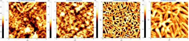
AFM studies. VDF 72% copolymer 100 nm-thick samples were subjected to different thermal conditions as mentioned in the previous section and their AFM images are shown in Fig. 1. Our emphasis is to prepare the highest possible flat surface with minimum deviation in film thickness in order to avoid the electrical breakdown. AC and AN samples exhibited much smaller crystalline size and relatively uniform film thickness as evidenced from their respective histograms (Figure not shown here). MQ and MSC samples exhibited drastically changed surface morphology with non-uniform film thickness.
(AC) |
(AN) |
(MQ) |
(MSC) |
Fig.1. AFM 2D-topography image (non-contact mode) of P(VDF/TrFE)(72/28) 100 nm ultrathin film as function of varying heat treatment conditions. Scanned area is 4Jm x 4Jm.
GIRAS Studies. GIRAS technique is sensitive to changes in crystallinity and chain orientation with varying thermal conditions as reported in our previous results [11]. In GIRAS used without a polarizer with the i.r. incident angle closer to grazing incident angle (ca 80~88o), it predominantly detects the vibrational modes with the transition dipoles normal to the substrate surface. Compared to AC sample (Fig. 2), the characteristic bands of trans-zigzag conformation of AN sample, for e.g. the
1289 cm-1 band(A1, ║b ) for the VDF trans sequence longer than TTTT, the 848 cm-1 band(A1,
║b ) for the trans sequence longer than TTT and 1182, 884 cm-1 bands(B2, ║a ) associated with crystalline phase show increase in the absorption intensity compared to MQ and MSC samples. The 1402 cm-1 (B1, ║c ) band assigned to ωCH2 coupled with νasC-C in which the transition moment is
along the chain direction was observed to decrease for AN sample.
After spin-casting, most polymer chains were preferentially oriented along the substrate surface
Solid State Phenomena Vols. 124-126 |
305 |
but still some chains exists in a random state, which after annealing, undergoes thermal relaxation resulting in preferential orientation of trans-zigzag chains parallel to the substrate surface. This results in decreasing B1 intensity along with increasing A1 and B2 crystalline peak intensities.
B 1
A 1
Absorbance
B1
A 1
1500 1400
B 2
B 2
A 1
A 1
MSC
MQ
AN
B 2
A 1
AC
|
|
|
|
B 2 |
A 1 |
|
|
|
|
|
|
1300 |
1200 |
1100 |
1000 |
900 |
800 |
W avenum ber (cm -1) |
|
|
|||
Fig. 2. FTIR-GIRAS measured at room temperature for VDF 72% copolymer 100 nm ultrathin film prepared under different thermal conditions.
This GIRAS data can be correlated with the uniform film surface observed from AC and AN AFM images and found to be the best method suitable for preparing samples with maximum dipole orientation along the poling direction. For MQ and MSC sample, there is some change in chain orientation along the normal to the surface plane resulting in an increase in B1 band intensity. With the preferential chain orientation for MQ and MSC samples parallel to the poling direction, it is almost impossible for the C-F dipoles to switch along the poling direction and hence unsuitable for device fabrication.
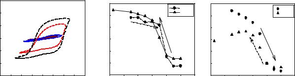
Electrical (P-E) studies. Fig. 3(a) shows the P-E hysteresis of VDF 72% copolymer 100 nm-thick AN film at 30oC as a function of varying external electric field. Under increasing external voltage, the C-F dipoles exhibit dielectric-to-ferroelectric behavior at and above 11 V.
Polarization( C/cm2)
15 |
|
5V |
|
|
|
|
|
|
|
1.2 |
|
|
|
|
|
|
6 |
|
|
|
|
|
|
|
|
|
|
|
|
|
|
|
|
|
|
|
|
|
|
|
|
|
|
|
|||
|
|
7V |
|
|
|
|
|
|
|
|
|
|
|
|
heating |
|
) |
|
|
|
|
heating |
|
10 |
|
9V |
|
|
|
|
|
|
|
|
|
|
|
|
cooling |
|
2 |
|
|
|
|
cooling |
|
|
|
|
|
|
|
|
|
1.0 |
|
|
|
|
|
|
|
|
|
|
|
||||
|
11V |
|
|
|
|
|
|
(MV/cm)FieldCoercive |
|
|
|
|
|
|
5 |
|
|
|
|
|
|||
|
|
|
|
|
|
|
|
|
|
|
|
|
|
|
|
|
|
|
|
||||
|
|
13V |
|
|
|
|
|
|
|
|
|
|
|
|
|
C/cmPolarization(Remnant |
|
|
|
|
|
|
|
5 |
|
15V |
|
|
|
|
|
|
|
0.8 |
|
heating |
|
|
|
|
4 |
|
|
|
|
|
|
|
|
17V |
|
|
|
|
|
|
|
|
|
|
|
|
|
|
|
|
|
|
|||
|
|
|
|
|
|
|
|
|
|
|
|
|
|
|
|
|
|
|
|
|
|
||
|
|
19V |
|
|
|
|
|
|
|
|
|
|
|
cooling |
|
|
|
|
|
|
|
|
|
0 |
|
|
|
|
|
|
|
|
|
0.6 |
|
|
|
|
|
|
3 |
|
|
|
heating |
|
|
|
|
|
|
|
|
|
|
|
|
|
|
|
|
|
|
|
|
|
|
|
|
||
-5 |
|
|
|
|
|
|
|
|
|
0.4 |
|
|
|
|
|
|
2 |
|
|
cooling |
|
|
|
-10 |
|
|
|
|
|
|
|
|
|
0.2 |
|
|
|
|
|
|
1 |
|
|
|
|
|
|
(a) |
|
|
|
|
|
|
|
|
(b) |
|
|
|
|
|
|
|
(c) |
|
|
|
|
|
|
-15 |
|
|
|
|
|
|
|
|
|
0.0 |
|
|
|
|
|
|
0 |
|
|
|
|
|
|
-20 |
-15 |
-10 |
-5 |
0 |
5 |
10 |
15 |
20 |
|
20 |
40 |
60 |
80 |
100 |
120 |
140 |
20 |
40 |
60 |
80 |
100 |
120 |
140 |
Biasvoltage(V) |
Temperature(oC) |
Temperature(oC) |
Fig.3. P-E curves observed for VDF 72% copolymer 100 nm-thick AN film (a) with varying external electric field under bias voltage at 30oC, (b) changes in Ec, and (c) changes in Pr as a function of heating-cooling.
Fig. 3(b) and (c) exhibit drastic changes in both Ec and Pr values during heating and cooling near the Tc range due to the phase transition between ferro (polar) ↔ paraelectric (non-polar) phase. From polarization studies, it is suggested that the data written in either '1' (+Pr) or '0' (-Pr) state can be read by applying bias DC or AC voltage below ±Ec on the basis of DC-EFM mode of SPM.
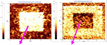
DC-EFM Studies. Fig. 4 shows the EFM amplitude images observed during (a) data write '1' state and (b) erase '0' state. Using EFM data, the change in dipole moment vectors along the applied field direction and the resultant change in amplitude or phase image for '1 or 0' state were monitored without causing any change in the surface morphology and hence has much wider and better WMRM
306 |
Advances in Nanomaterials and Processing |
|
|
storage applications than that mentioned in Ref. [1,2].
|
|
|
|
|
|
|
|
(a) |
(b) |
||
Fig. 4. EFM amplitude images of VDF 72% copolymer 250 nm film; (a) data written (Tip bias voltage: +20V) and
(b) data erased by switching the voltage in the opposite direction (Tip bias voltage: -20V).
Conclusions
In this paper, we have used SPM based technique to observe the surface topology and demonstrate the piezoelectricity in VDF 72% copolymer ultrathin films. AFM and FTIR-GIRAS were complementary in analyzing surface crystalline morphology and the resultant change in chain orientation with varying thermal history. Among different thermal conditions studied, the as-cast annealed sample was found to be most suitable for device fabrication having preferential dipole orientation along the poling direction and used in our further studies. DC-EFM technique can be used to 'write-read-erase' the data on the memory bit in a much faster time. From these results, we were able to have a good understanding of the ferroelectric and piezoelectric behavior of P(VDF/TrFE)(72/28) ultrathin films suitable for futuristic SPM based high density data storage applications.
Acknowledgement. This study was supported by Korea Ministry of Commerce, Industry and Energy’ (Project No 10022983-2004-11) and Korea Science and Engineering Foundation (KOSEF) through the SRC/ERC Program of MOST/KOSEF (R11-2005-065).
References
[1]C.S. Lee, H.J. Nam, Y.S. Kim, W.H. Jin, S.M. Cho and J.U. Bu: Appl. Phys. Lett. Vol. 83 (2003), p. 4839.
[2]H.J. Nam, S. Jang, Y.S. Kim, C.S. Lee, W.H. Jin, I.J. Cho and J.U. Bu: J. Semicon. Technol. Sci. Vol.5 (1) (2005), p. 24.
[3]A.J. Lovinger, G.T. Davis, T. Furukawa and M.G. Broadhurst: Macromolecules Vol. 15 (1982), p. 323.
[4]K. Tashiro and M. Kobayashi: Phase Trans. Vol. 18 (1989), p. 213.
[5]A. Bune, V. Fridkin, S. Ducharme, L. Blinov, S. Palto, A.V. Sorokin, S. Yudin and A. Zlatkin: Nature Vol. 391 (1998), p. 874.
[6]K. Hami, M. Hara, H. Yamada and K. Matsushige: Ann. Chim. Sci. Mat. Vol. 26 (2001), p. 217.
[7]Q.M. Zhang, H. Xu, F. Fang, Z.Y. Cheng and F. Xia, J. Appl. Phys. Vol. 89 (2001), p. 2613.
[8]T.J. Reece, S. Ducharme, A.V. Sorokin and M. Poulsen: Appl. Phys. Lett. Vol. 82 (2003), p. 142.
[9]K. Noda, K. Ishida, A. Kubono, T. Horiuchi, H. Yamada and K. Matsushige: J. Appl. Phys. Vol. 93 (5) (2003), p. 2866.
[10]K. Tashiro and M. Kobayashi: Spectrochim. Acta Vol 50A (1994), p. 1573.
[11]A.A. Prabu, J.S. Lee, K.J. Kim and H.S. Lee: Vib. Spec. Vol. 41 (2006), p. 1.
Advances in Nanomaterials and Processing
10.4028/www.scientific.net/SSP.124-126
Ferroelectric P(VDF/TrFE) Ultrathin Film for SPM-Based Data Storage Devices
10.4028/www.scientific.net/SSP.124-126.303
DOI References
[3]A.J. Lovinger, G.T. Davis, T. Furukawa and M.G. Broadhurst: Macromolecules Vol. 15 1982), p. 323. doi:10.1021/ma00230a024
[5]A. Bune, V. Fridkin, S. Ducharme, L. Blinov, S. Palto, A.V. Sorokin, S. Yudin and A. latkin: Nature Vol. 391 (1998), p. 874.
doi:10.1038/36069
[8]T.J. Reece, S. Ducharme, A.V. Sorokin and M. Poulsen: Appl. Phys. Lett. Vol. 82 (2003), p. 42. doi:10.1063/1.1533844
[3]A.J. Lovinger, G.T. Davis, T. Furukawa and M.G. Broadhurst: Macromolecules Vol. 15 (1982), p. 323. doi:10.1021/ma00230a024
[4]K. Tashiro and M. Kobayashi: Phase Trans. Vol. 18 (1989), p. 213.
doi:10.1080/01411598908206864
[8] T.J. Reece, S. Ducharme, A.V. Sorokin and M. Poulsen: Appl. Phys. Lett. Vol. 82 (2003), p. 142.
doi:10.1063/1.1533844
[11] A.A. Prabu, J.S. Lee, K.J. Kim and H.S. Lee: Vib. Spec. Vol. 41 (2006), p. 1.
doi:10.1016/j.vibspec.2005.11.005