

Smart Mater. Struct. 20 (2011) 087001 |
|
|
Technical Note |
||||||||||||||
|
|
|
|
|
|
|
|
|
|
|
|
|
|
|
|
|
|
|
|
|
|
|
|
|
|
|
|
|
|
|
|
|
|
|
|
|
|
|
|
|
|
|
|
|
|
|
|
|
|
|
|
|
|
|
|
|
|
|
|
|
|
|
|
|
|
|
|
|
|
|
|
|
|
|
|
|
|
|
|
|
|
|
|
|
|
|
|
|
|
|
|
|
|
|
|
|
|
|
|
|
|
|
|
|
|
|
|
|
|
|
|
|
|
|
|
|
|
|
|
|
|
|
|
|
|
|
|
|
|
|
|
|
|
|
|
|
|
|
|
|
|
|
|
|
|
|
|
|
|
|
|
|
|
|
|
|
|
|
|
|
|
|
|
|
|
|
|
|
|
|
|
|
|
|
|
|
|
|
|
|
|
|
|
|
|
|
|
|
|
|
|
|
|
|
|
|
|
|
|
|
|
|
|
|
|
|
|
|
|
|
|
|
|
|
|
|
|
|
|
|
|
|
|
|
|
|
|
|
|
|
|
|
|
|
|
|
|
|
|
|
|
|
|
|
|
|
|
|
|
|
|
|
|
|
|
|
|
|
|
|
|
|
|
|
|
|
|
|
|
|
|
|
|
|
|
|
|
|
|
|
|
|
|
|
|
|
|
|
|
|
|
|
|
|
|
|
|
|
|
|
|
|
|
|
|
|
|
|
|
|
|
|
|
|
|
|
|
|
|
|
|
|
|
|
|
|
|
|
|
|
|
|
|
|
|
|
|
|
|
|
|
|
|
|
|
|
|
|
|
|
|
|
|
|
|
|
|
|
|
|
|
|
|
|
|
|
|
|
|
|
|
|
|
|
|
|
|
Figure 9. Development of the ferroelectric properties of the deposited 1 μm thick P(VDF–TrFE) films annealed at 125 ◦ C throughout the outlined process flow given in figure 7.
with the definition of the top electrode (step F) and closing with the released device (step L). Failure to protect the P(VDF– TrFE) layer during device release (that means including step J) becomes clearly apparent in the properties of the released device.
The developed process flow for PVDF-based microsystems has now been applied to the fabrication of a common proof mass device. Effectively, the preliminary backside etching of the silicon wafer is analogously performed but leaves out a cylindrical proof mass as discussed in the introduction. The subsequently defined P(VDF–TrFE) stacks now bear this proof mass with a thickness of about 450 μm after device release. An optical microscopy image of a complete device is shown in figure 10.
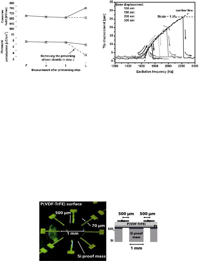
The structural integrity of the released device can be demonstrated by mechanically inducing a resonant vibration via a piezoelectric shaker. Monitoring the vibration characteristics of this device under different base displacements (shown in figure 11) results in a hysteretic response characteristic for a Duffing oscillator with a
Figure 11. Nonlinear frequency response of the device shown in figure 10 for different base displacements and sweeps of the excitation frequencies. The device operates in a nonlinear stretching-determined regime and the maximum induced stretching can be approximated to be about 1.5 .
pronounced nonlinearity. The maximum induced strain state can be approximated to be about 1.5 and was at this point limited by device damping effects and the resolution of the applied vibrometer.
In total, the strongly elastic nature of the P(VDF–TrFE) in combination with the ductile properties of the metallization layers easily allow a strain state to be approached during device operation that is already beyond the brink of the device failure which has been experienced for similarly prepared ceramicbased microsystems.
4. Conclusions
In summary, lithographical pattern transfer to P(VDF– TrFE) films were found to be eligible if certain restrictions are accounted for which is largely unusual for polymeric substances. With respect to this, a thorough investigation of the damage potential of the exposure to chemicals during
Figure 10. Microscopy image and schematic cross-section of a common proof mass device fabricated using the platinum–P(VDF–TrFE)–gold stacks for the suspending beams attached to the silicon proof mass. The spatial dimensions of the device are indicated in the image with the exception of the height of the proof mass which is about 450 μm and the thickness of the suspending beams as shown in figure 8.
7
Smart Mater. Struct. 20 (2011) 087001 |
Technical Note |
lithography as well as of the applied reactive ion etching steps has been performed and resulted in a corresponding microsystem fabrication process. Hence, the inherent material advantages could be transferred to a functional device rendering novel strongly strain-based device designs as in piezoelectric microgenerators feasible. The prepared devices were indeed found to be highly insusceptible to stretching induced material failure and featured a nonlinear resonance as expected. Points that should still be addressed include fostering understanding as to why lithographical pattern transfer is altogether possible for this polymeric system and how the fabrication process can be improved. Several process variables that seem to contribute to these questions have been identified in this work. Furthermore, the remaining metal electrodes could be exchanged for polymeric electrodes in a concluding step to fully tap the potential of a strain-based microsystem design and evade the possible impact of intrinsic material stresses. Finally, future research should theoretically assess whether exchanging higher strain levels for lower piezoelectric coupling coefficients can lead to improved device performance. However, no static comparison may be performed but the possibility to obtain unequaled strain levels during operation has to be taken into account which may imply a complete redesign of the respective devices.
Acknowledgments
This work was supported by the Hans. L Merkle Foundation for the Association for the Promotion of Science and Humanities in Germany (Grant T 113/16679/07).
References
[1]Roundy S, Wright P K and Rabaey J 2003 A study of low level vibrations as a power source for wireless sensor nodes
Comput. Commun. 26 1131–44
[2]Pereyma M 2007 Overview of the modern state of the vibration energy harvesting devices MEMSTECH pp 107–12
[3]Erturk A and Inman D J 2011 Piezoelectric Energy Harvesting
1st edn (New York: Wiley)
[4]Cook-Chennault K A, Thambi N and Sastry A M 2008 Powering MEMS portable devices—a review of non-regenerative and regenerative power supply systems with special emphasis on piezoelectric energy harvesting systems Smart Mater. Struct. 17 043001
[5]Yan Z and He Q 2011 A review of piezoelectric vibration generator for energy harvesting Appl. Mech. Mater. 44–47 2945–9
[6]Jeon Y B, Sood R, Jeong J and Kim S G 2005 MEMS power generator with transverse mode thin film PZT Sensors Actuators A 122 16–22
[7]Choi W J, Jeon Y, Jeong J H, Sood R and Kim S G 2006 Energy harvesting MEMS device based on thin film piezoelectric cantilevers J. Electroceram. 17 543–8
[8]Hajati A and Kim S-G 2008 Rectifier-less piezoelectric micro power generator Active and Passive Smart Structures and Integrated Systems Proc. SPIE 6928 69281T
[9]Shen D, Park J-H, Ajitsaria J, Choe S-Y, Wikle H C and
Kim D-J 2008 The design, fabrication and evaluation of a MEMS PZT cantilever with an integrated Si proof mass for vibration energy harvesting J. Micromech. Microeng.
18 055017
[10]Cottone F, Vocca H and Gammaitoni L 2009 Nonlinear energy harvesting Phys. Rev. Lett. 102 080601
[11]Adhikari S, Friswell M I and Inman D J 2009 Piezoelectric energy harvesting from broadband random vibrations Smart Mater. Struct. 18 115005
[12]Erturk A, Hoffmann J and Inman D J 2009 A piezomagnetoelastic structure for broadband vibration energy harvesting Appl. Phys. Lett. 94 254102
[13]Marinkovic B and Koser H 2009 Smart sand—a wide bandwidth vibration energy harvesting platform Appl. Phys. Lett. 94 103505
[14]Hajati A and Kim S-G 2009 Wide-bandwidth MEMS-scale piezoelectric energy harvester Proc. Power MEMS
[15]Dargaville T R, Celina M C, Elliott J M, Chaplya P M,
Jones G D, Mowery D M, Assink R A, Clough R L and Martin J W 2005 Characterization, Performance and Optimization of PVDF as a Piezoelectric Film for Advanced Space Mirror Concepts Sandia report SAND2005-6846
[16]Furukawa T, Takahashi Y and Nakajima T 2010 Recent advances in ferroelectric polymer thin films for memory applications Curr. Appl. Phys. 10 e62–7
[17]Ebnesajjad S 2003 Fluoroplastics vol 2 Plastics Design Library
[18]Siviour C R, Walley S M, Proud W G and Field J E 2005 The high strain rate compressive behaviour of polycarbonate and polyvinylidene difluoride Polymer 46 546–55
[19]Shen D N, Choe S Y and Kim D J 2007 Analysis of piezoelectric materials for energy harvesting devices under high-g vibrations Japan. J. Appl. Phys. 46 6755–60
[20]Manohora H M, Morikawa E, Choi J and Sprunger P T 1999 Pattern transfer by direct photo etching of PVDF using x rays J. Microelectromech. Syst. 8 417–22
[21]Ye Y-H, Jeong D-Y and Zhang Q M 2004 Fabrication of strain tunable infrared frequency selective surfaces on electrostrictive P(VDF-TrFE) copolymer films using a stencil mask method Appl. Phys. Lett. 85 654–6
[22]Zhang L, Ducharme S and Li J 2007 Microimprinting and ferroelectric properties of P(VDF-TrFE) copolymer films
Appl. Phys. Lett. 91 172906
[23]Gallego D, Ferrell N J and Hansford D J 2007 Fabrication of piezoelectric PVDF microstructures by soft lithography for tissue engineering and cell biology applications Mater. Res. Soc. Symp. Proc. 1002
[24]Tang Q, Shi S-Q, Huang H and Zhou L M 2004 Fabrication of highly oriented microstructures and nanostructures of ferroelectric P(VDF-TrFE) copolymer via dip-pen nanolithography Superlatt. Microstruct. 36 21–9
[25]Spierings G A C M, Dormans G J M, Moors W G J,
Ulenaers M J E and Larsen P K 1995 Stresses in Pt/Pb(Zr,Ti) O3/Pt thin-film stacks for integrated ferroelectric capacitors
J. Appl. Phys. 78 1926–33
[26]Gerber P, Roelofs A, Lohse O, Kugeler C, Tiedke S, Boettger U and Waser R 2003 Short-time piezoelectric
measurements in ferroelectric thin films using a double-beam laser interferometer Rev. Sci. Instrum. 74 2613–5
[27]Hasegawa R, Takahashi Y, Chatani Y and Tadokoro H 1972 Crystal structures of three crystalline forms of poly(vinylidene fluoride) Polym. J. 3 600–10
[28]Hasegawa R, Kobayashi M and Tadokoro H 1972 Molecular conformation and packing of poly(vinylidene fluoride). Stability of three crystalline forms and the effect of high pressure Polym. J. 3 591–9
[29]Gerber P, Boettger U and Waser R 2006 Composition influences on the electrical and electromechanical properties of lead zirconate titanate thin films J. Appl. Phys.
100 124105
8