

Avr242: 8-bit Microcontroller Multiplexing led Drive and a 4 X 4 Keypad

Рисунок 22 – Circuit Diagram for Keypad/Display Unit
Theory of Operation
The connection of a 4 x 4 keypad, a piezo sounder, two LED loads and a four digit multiplexed display, would normally require twenty-three I/O lines. This application shows how this can be reduced to fifteen with a bit of ingenuity, allowing the smaller 20-pin AVR to be used. The circuit diagram is shown in figure 1 and is complete apart from the oscillator components, which have been omitted for clarity. The four keypad columns are connected to the low nibble of port B and the four keypad rows are connected to the high nibble. The same eight bits also directly drive the segment cathodes of the four digit LED display, via current limit resistors R13-20. The pins thus serve a dual function, acting as outputs when driving the LED display and I/O when scanning the keypad. This is accomplished by using the programmable nature and large current drive capabilities of the AVR ports to good effect. The majority of the time port B sinks the 9 mA of current, to directly drive the LED segments . Each digit is switched sequentially in 5 ms time slots, to multiplex the displays via the PNP transistors Q1-4. The common anodes of the LED display digits are driven via PNP transistors, since the maximum possible 72 mA (9mA - 8 segments) of current is outside the handling capabilities of the ports. These can be any PNP type capable of driving 100 mA or so (e.g BC479). This could be modified by paralleling up two port pins for each anode to share the current, but then the number of I/O pins required would necessitate the use of a larger MCU. Before the start of each display cycle, the port configuration is changed to provide four inputs with internal pull-ups enabled, and four outputs in the low state to scan the keypad. If a key is pressed the nibble configuration is transposed to calculate the key value with the key number stored in a variable. A short delay is allowed between each port change to allow the port to settle. This method is more code efficient than the conventional “snake” method in this application. The common anode drives are disabled during this time to avoid interference. The port configuration is then reinstated ready for the multiplexing routine. The main housekeeping function then uses this key variable to take the appropriate action.
The real time clock is interrupt driven, using Timer 0 clocked from the system clock divided by 256. The timer is preloaded with the number 176 and interrupts on overflow every five milliseconds, ensuring high accuracy if a good quality crystal is used. To be accurate a 4.096 MHz clock crystal is employed. The program could be modified to use a 4 MHz crystal with minor modifications. The interrupt service routine reloads the timer and increments three variables: a counter variable (tock), a keypad debounce variable (bounce) and a counter to maintain the seconds count (second). This is used by the main housekeeping function to update the minutes and hours, which in turn are displayed by the display function.
The housekeeping function checks the two loads for ON or OFF times and controls the outputs on the high nibble of port D accordingly. In this application the loads are simulated by red and green LEDs driven in current sink (active low) configuration. These could be replaced by relay drivers or optocoupled triacs to drive power loads. The keypad provides a means of setting up (SET) the real time and the ON/OFF times of each load and also allows the loads to be turned off (CLEAR) at once. A Piezo sounder, connected to the top bit of port D, provides an udible beep on key press.
The use of the port B pins requires some careful consideration. Since the pins are used for two functions, it is important that if a key is pressed, it does not short out the display. This is achieved by placing current limit resistors in series with each key. When used as inputs the internal pull-up resistors are employed saving external components. The choice of resistor value (R1-8) is such that the potential division is negligible. With the values chosen, and on a 5V supply, the logic levels are about 0.6V for logic “0” and 4.95V for logic “1”. Resistors R21 and R22 are the traditional current limit resistors for the LEDs and can be any suitable value for the supply rail. This note was tested using 330 ohms on a 5V supply. The LEDs are driven in current sink mode (“0” = ON) and provide about 9 mA of forward current with the values specified.

Рисунок 23 – Keypad and LED connections (AVR240: 4 x 4 Keypad – Wake up on Keypress)
This application note describes a simple interface to a 4 x 4 keypad designed for low power battery operation. The AVR spends most of its time in power down mode, waking up when a key is pressed to instigate a simple test program that flashes one of two LEDs according to the key pressed. If 0 (zero) is pressed the RED LED flashes 10 times. All other keys flash the GREEN LED the number of times marked on the key (e.g. if “C” is pressed the GREEN LED flashes twelve times).
Theory of Operation
The keypad columns are connected to the high nibble of port B. The keypad rows are connected to the low nibble. Resistors R1 to R8 serve to limit input current to a safe level in the event of ESD from the keypad. They can be omitted in most applications. In the steady state condition the high nibble is configured as outputs and are in the low state. The low nibble is configured as inputs and has the internal pull ups enabled, removing the need for external pull-up resistors. After initialization the AVR is put to sleep. When a key is pressed one of the diodes D1-D4 pull down the external interrupt line PD2, which also has internal pull-ups enabled. This wakes up the AVR and causes it to run the interrupt service routine which scans the keypad and calculates which key is pressed. It then returns to the main program and drives the LEDs according to the key pressed, putting the AVR back to sleep when it has finished.
Resistors R9 and R10 are the traditional current limit resistors for the LEDs and can be any suitable value for the supply rail. This application note was tested using 330 ohms on a 5v supply. The LEDs are driven in current sink mode (“0” = ON) and provide about 10 mA of forward current with the values specified.

Рисунок 24 – ИК приемник дистанционного управления (AVR410: RC5 IR Remote Control Receiver)
Most audio and video systems are equipped with an infra-red remote con- trol. This application note describes a receiver for the frequently used Philips/Sony RC5 coding scheme. The RC5 code is a 14-bit word bi-phase coded signal. The two first bits are start bits, always having the value 1. The next bit is a control bit or toggle bit, which is inverted every time a button is pressed on the remote control transmitter. Five system bits hold the system address so that only the right system responds to the code. Usually, TV sets have the system address 0, VCRs the address 5 and so on. The command sequence is six bits long, allowing up to 64 different commands per address. The bits are transmitted in bi-phase code (also known as Manchester code). An example where the command 0x35 is sent to system 5.
The Detect Subroutine (Synchronizing and sampling of the data)
When
the detect subroutine is called, it first waits for the data line to
be idle high for more than 3.5 ms. Then, a start bit can be detected.
The length of the low part of the first start bit is measured. If no
start bit is detected within 131 ms, or if the low pulse is longer
than 1.1 ms, the routine returns indicating no command received.
The measurement of the start bit is used to calculate two reference times, ref1 and ref2, which are used when sampling the data line. The program uses the edge in the middle of every bit to synchronize the timing. 3/4 bit length after this edge, the line is sampled. This is in the middle of the first half of the next bit (see Figure 5). The state is stored and the routine waits for the middle edge. Then, the timer is synchronized again and everything is repeated for the following bits. If the synchronizing edge is not detected within 5/4 bit times from the previous synchronizing edge, this is detected as a fault and the routine terminates. When all the bits are received, the command and system address are stored in the “command” and “system” registers. The control bit is stored in bit 6 of “command”.
Схема формирования DTMF сигнала (DTMF Tone Generation Using the Z86E04 MCU) – рисунок 25:

The program outlined below generates DTMF tones using a pulse width modulation (PWM) algorithm. PWM is used to vary the DC level of the output by varying the duty cycle (the "on" time divided by the cycle period) of the square wave. Varying the "on" time by a sine function and then feeding the output through a low pass filter yields a sine wave.
The sine table contains 256 entries, which in turn contain hexadecimal values representing a sine function for 360 degrees. These values are indexed and loaded
into T1 at a sampling rate that, according to Nyquist, must be at least twice the highest frequency tone that we want to reproduce. Since the highest frequency for this application is 1477 Hz, the sampling rate must be at least twice this, or 2954 samples per second. The higher the sampling rate, the greater the accuracy. In the example
illustrated here a sample rate of 12000 samples per second is used both for higher accuracy and ease in filtering.
Since we are, in effect, producing two tones, two pointers are used to fetch the next value in the look-up table: one for row frequencies, and one for column frequencies. The frequency of the resulting sine wave can be calculated by multiplying
the number of steps in the sine look-up table (256) by the desired frequency, divided by the sampling rate. This offset value is added to the current pointer, which then fetches the next hex number from the look-up table. This is done for both the row and column frequencies. The two are added, then loaded into the timer register (T1).
The low pass filter was chosen to have a corner frequency of the lowest column frequency, or 1209 Hz. At this point, the column frequencies will be at least 3 dB below the row frequencies. However, telephone lines themselves act as a large-scale low pass filter, and by the time the tones reach the telephone switching equipment, the amplitude should be the same. The spec therefore calls for the column frequencies to be 3 dB higher than the row frequencies. In the telephone industry this is known as "twist."
This adjustment can be made in software by taking the hex value from the look-up table for the column frequency and doing a "rotate left." This results in twice the amplitude for the column frequency — 6 dB gain, or 3 dB up from the row frequency, just where we want to be. Overall dB level from the output of the low pass filter can be adjusted with a potentiometer.
Схема формирования DTMF сигнала (DTMF Tone Generation Using the Z86E04 MCU) – рисунок 26:

DTMF signals are a combination of two sine waves of different frequencies that correspond to a row and column position on the standard telephone keypad. To produce the twelve key tones of this keypad, seven sine-wave frequencies are required. Three frequencies are associated with the column positions and four with the row positions. Each key is associated with a corresponding pair of tones that are produced when the key is selected. For example, assume the 0 key is pressed. The row frequency would be 941 Hz while the column frequency would be 1336 Hz. These two frequencies, or tones, are added together to produce the signal understood at the receiving end to be the 0 key.
The standard telephone keypad and the corresponding DTMF tone assignments are indicated in Table.
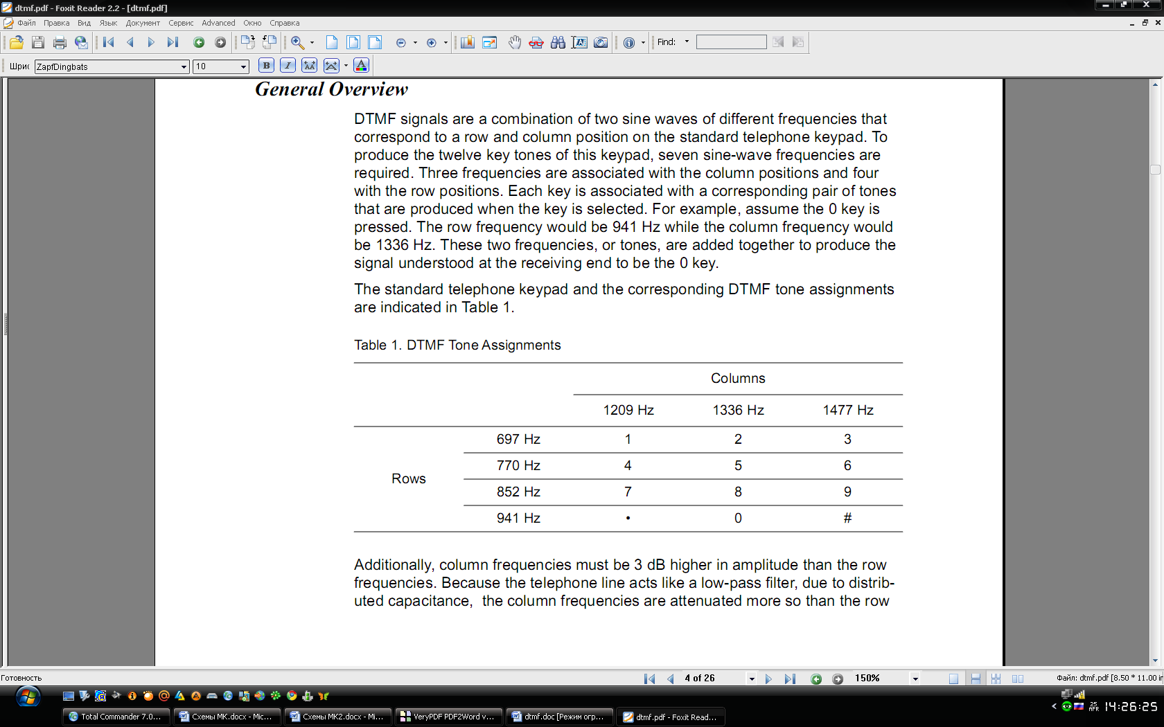
Additionally, column frequencies must be 3 dB higher in amplitude than the row frequencies. Because the telephone line acts like a low-pass filter, due to distributed capacitance, the column frequencies are attenuated more so than the row frequencies. The 3-db column-frequency boost is a compensation for this line characteristic.
DTMF Tone Generation
DTMF tones are specific pairs of sine waves, produced simultaneously, that represent the key positions of a common telephone keypad. Adding the individual sine waves together produces the DTMF. In this case, the generation of each sine wave is related to a timer value, one for the column and one for the row frequency. Before the column sine value is added to the row sine value, the column value is doubled by shifting left one time. This new value provides the 3 dB edge over the row frequencies. The range of values in the sine table becomes more meaningful because, for the worst case, the sine value may be three times larger before using this value for the 8-bit counter.
Схема телефонной трубки DTMF сигнала (Telephone Handset with DTMF using the 68HC05F4)


Рисунок 27 – Схема телефонной трубки DTMF сигнала
Рисунок 28 – Блок схема

Рисунок 29 – Схема

Рисунок 30 – Схема управления фазой (Power Phase Control Using Z8 Microcontrollers)
Theory of Operation
This design involves the load control circuit illustrated in the schematic. This circuit is comprised of a low cost AC/DC converter, AC zero crossing detection, power increase and decrease buttons, and a load switching Triac. The Z8 microcontroller senses AC zero crossing on port 3. The port 3 pins provide an interrupt on a falling edge input. A falling edge on port 3 signals the start of an AC cycle on the source waveform. The Z8 comparator interrupt routine sets a flag signaling the source waveform phase. The Z8 also loads a time and desired power control level through the pushbuttons and controls the AC fire control angle to the Triac to implement power control. This design is based on the fact that a Triac conducts until the next zero crossing when it receives a pulse on its input. The Z8 microcontroller controls the firing angle in the AC source waveform in a pulse to the Triac. The user modifies the firing angle (desired power angle) by selecting an up key or down key to increase or decrease power to the load. The design incorporates a low cost AC/DC voltage regulator. The design uses an AC source voltage zero crossing circuit. The zero crossing circuit functions independent of source voltage.
The Z8 microcontroller code in this application scans the source 60-Hz rectangle input on Port P32. On every falling edge of P32 an interrupt request occurs. In the interrupt service routine, timer T1 is loaded with a hold-off value. The longer the hold-off time, the less power is driven to the load. The shorter the hold off time, more of the AC waveform is realized at the load, increasing the power delivered to the load.
When timer T1 times out, another interrupt is generated. In the T1 interrupt service routine the Triac is given an ignition pulse. The Triac conducts until the next zero crossing of the source waveform. In a 60-Hz system a zero crossing occurs every 8.33 mS. After 8.33 mS, the T1 timer is re-loaded with the ignition hold-off time. When the T1 timer expires, the Triac receives another ignition pulse to turn ТONУ for the next cycle of the waveform. This cycle repeats on each waveform.
The scan key subroutine is called in each T1 interrupt routine. A valid push is detected if scan key detects a valid key push in eight consecutive T1 interrupts. To attain multiple valid key pushes, the scan key subroutine debounces and filters the key inputs.
The Soft Start option ramps the AC source power to the load by steadily increasing Triac on-time. This feature lengthens the lifetime of light bulbs and other loads by controlling the turn-on power.
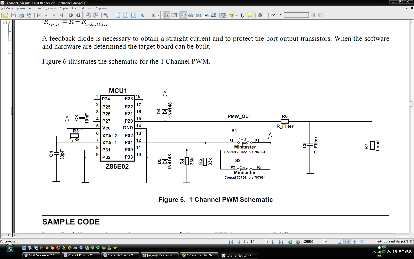
Рисунок 31 – Канал широтно-импульсной модуляции (1 Channel DAC Using A PWM)
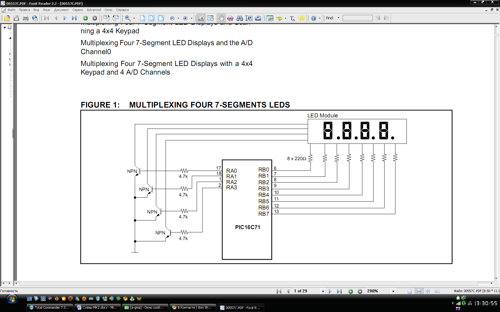
Рисунок 32 – Схема мультиплексирования (Multiplexing Four 7-segments LEDs)

Рисунок 33 – Схема мультиплексирования с клавиатурой 4 на 4
(Multiplexing Four 7-segments LEDs with a 4 x 4 Keypad)
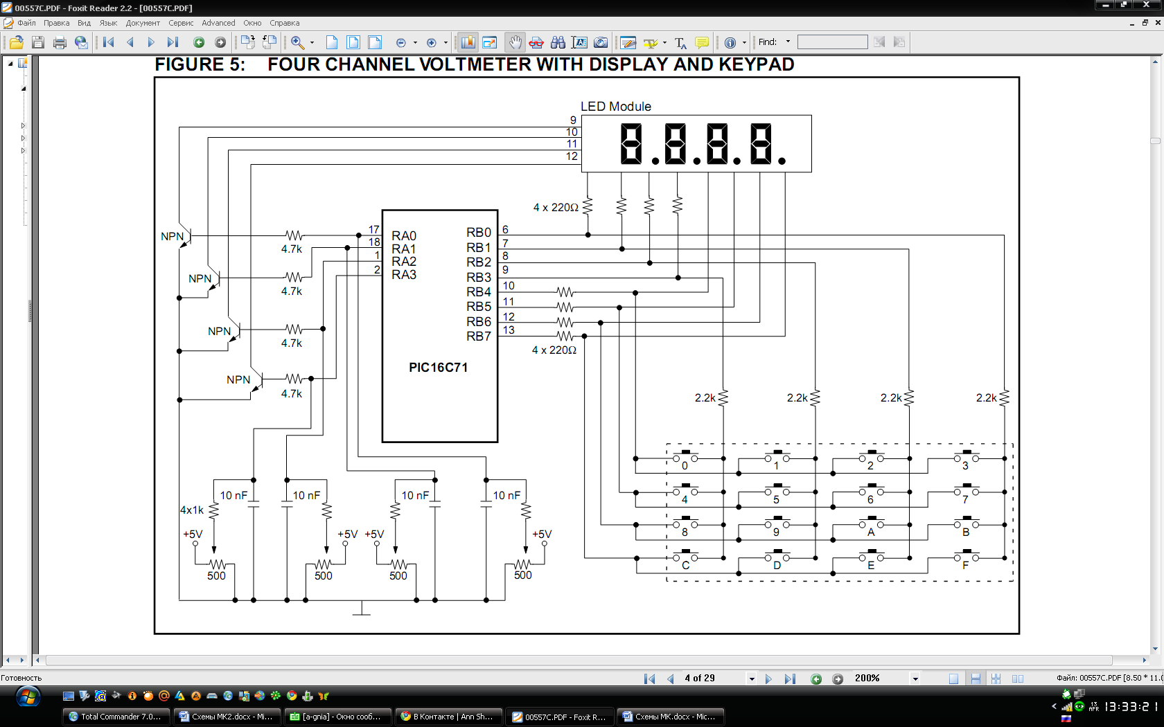
Рисунок 34 – 4х канальный вольтметр с клавиатурой и дисплеем
(Four Channel Voltmeter with Display And Keypad)

Рисунок 35 – SRAM Block Schematic (STK 501)
The A16 pin on the PORTG/AUX connector is connected to A16 (address pin 16) on the SRAM. ATmega103(L) and ATmega128(L) support up to 60 KB of external SRAM. The STK501 SRAM footprint is for a 128 KB SRAM. Implementing software control of the A16 line will increase the memory range from 64 KB to 128 KB. This line is pulled low by default, addressing the lower 64 KB of the SRAM.

Рисунок 36 – Схема
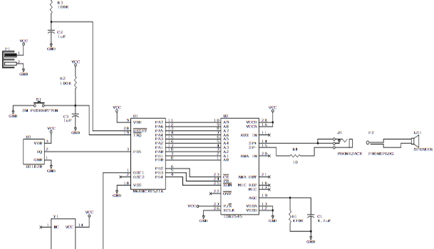
Рисунок 37 – Схема звукового термометра (Audible Thermometer Schematics)
Автоматический регулятор напряжения:

Рисунок 38 – Схема автоматического регулятора напряжения