

Jones D.PCB design tutorial.2004
.pdfPCB Design Tutorial by David L. Jones
connection on your board with the schematic, net by net. Highlight each net on the schematic as you complete it. When you are finished, there should be no electrical connections left that aren’t highlighted. You can now be fairly confident that your board is electrically correct.
Basic Routing
Now it’s time for some basic routing rules. Routing is also known as “tracking”.
Routing is the process of laying down tracks to connect components on your board. An electrical connection between two or more pads is known as a “net”.
ØKeep nets as short as possible. The longer your total track length, the greater it’s resistance, capacitance and inductance. All of which can be undesirable factors.
ØTracks should only have angles of 45 degrees. Avoid the use of right angles, and under no circumstances use an angle greater than 90 degrees. This is important to give a professional and neat appearance to your board. PCB packages will have a mode to enforce 45 degree movements, make use of it. There should never be a need to turn it off. Contrary to popular belief, sharp right angle corners on tracks don’t produce measurable EMI or other problems. The reasons to avoid right angles are much simpler - it just doesn’t look good, and it may have some manufacturing implications.
ØForget nice rounded track corners, they are harder and slower to place and have no real advantage. Stick to 45 degree increments. Rounded track bends belong to the pre-CAD taped artwork era.
Ø“Snake” your tracks around the board, don’t just go “point to point”. Point to point tracking may look more efficient to a beginner at first, but there are a few reasons you shouldn’t use it. The first is that it’s ugly, always an important factor in PCB design! The second is that it is not very space efficient when you want to run more tracks on other layers.
ØEnable your Electrical grid, which is sometimes referred to as a “snap to center” or “snap to nearest” option. Let the software find the centers of pads and ends of tracks automatically for you. This is great for when you have pads and tracks which aren’t lined up to your current snap grid. If you don’t have these options enabled then you may have to keep reducing your snap grid until you find one that fits. Far more trouble than it’s worth. There is almost never a reason to have these options disabled.
ØAlways take your track to the center of the pad, don’t make your track and pad “just touch”. There are few reasons for this. The first is that it’s sloppy and unprofessional. The second is that your program may not think that the track is making electrical connection to the pad. Proper use of a snap grid and electrical grid will avoid problems here.
ØUse a single track, not multiple tracks tacked together end to end. It may make no difference to the look of your final board, but it can be a pain for future editing. Often you’ll have to extend a track a bit. In this case it’s best to delete the old one and place a new one. It may take a few extra seconds, but it’s worth it. People looking at your finished board may not know, but YOU’LL know! It’s the little touches like this that set good PCB designers apart.
ØMake sure your tracks go right through the exact center of pads and components, and not off to one side. Use of the correct snap grid will ensure that you get this right every time. If your track doesn’t go through the exact center then you are using the wrong snap grid. Why do you need to do this? It makes your board neater and more symmetrical, and it gives you the most clearance.
ØOnly take one track between 100 thou pads unless absolutely necessary. Only on large and very dense designs should you consider two tracks between pads. Three tracks between pads is not unheard of, but we are talking seriously fine tolerances here.
ØFor high currents, use multiple vias when going between layers. This will reduce your track impedance and improve the reliability. This is a general rule whenever you need to decrease the impedance of your track or power plane.
ØDon’t “drag” tracks to angles other than 45 degrees
Ø“Neck down” between pads where possible. Eg, a 10 thou track through two 60 thou pads gives a generous 15 thou clearance between track and pad.
ØIf your power and ground tracks are deemed to be critical, then lay them down first. Also, make your power tracks as BIG as possible.
Page 11 of 25
PCB Design Tutorial by David L. Jones
ØKeep power and ground tracks running in close proximity to each other if possible, don’t send them in opposite directions around the board. This lowers the loop inductance of your power system, and allows for effective bypassing.
ØKeep things symmetrical. Symmetry in tracking and component placement is really nice from a professional aesthetics point of view.
ØDon’t leave any unconnected copper fills (also called “dead copper”), ground them or take them out.
If you are laying out a non-plated through double sided board, then there are some additional things to watch out for. Non-plate through holes require you to solder a link through the board on both the top and bottom layer.
∙Do not place vias under components. Once the component is soldered in place you won’t be able to access the joint to solder a feed through. The solder joint for the feed through can also interfere with the compnent.
∙Try and use through hole component legs to connect top tracks to bottom tracks. This minimises the number of vias. Remember that each via adds two solder joints to your board. The more solder joints you have, the less reliable your board becomes. Not to mention that that it takes a lot longer to assemble.
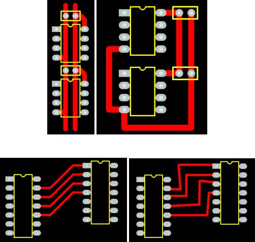
An example of GOOD power routing (Left) and BAD power routing (Right)
An example of GOOD routing (Left) and BAD routing (Right)
Page 12 of 25

PCB Design Tutorial by David L. Jones
Finishing Touches
Once you have finished all your routing, your board isn’t done quite yet. There are a few last minute checks and finishing touches you should do.
ØIf you have thin tracks (<25 thou) then it’s nice to add a “chamfer” to any “T” junctions, thus eliminating any 90 degree angles. This makes the track more physically robust, and prevents any potential manufacturing etching problems. But most importantly, it looks nice.
ØCheck that you have any required mounting holes on the board. Keep mounting holes well clear of any components or tracks. Allow room for any washers and screws.
ØMinimise the number of hole sizes. Extra hole sizes cost you money, as the manufacturer will charge you based on not only the number of holes in your boards, but the number of different hole sizes you have. It takes time for the very high speed drill to spin down, change drill bits, and then spin up again. Check with your manufacturer for these costs, but you can’t go wrong by minimising the number of hole sizes.
ØDouble check for correct hole sizes on all your components. Nothing is more annoying than getting your perfectly laid out board back from the manufacturer, only to find that a component won’t fit in the holes! This is a very common problem, don’t get caught out.
ØEnsure that all your vias are identical, with the same pad and hole sizes. Remember your pad to hole ratio. Errors here can cause “breakouts” in your via pad, where the hole, if shifted slightly can be outside of your pad. With plated through holes this is not always fatal, but without a complete annular ring around your hole, your via will be mechanically unreliable.
ØCheck that there is adequate physical distance between all your components. Watch out for components with exposed metal that can make electrical contact with other components, or exposed tracks and pads.
ØChange your display to “draft” mode, which will display all your tracks and pads as outlines. This will allow you to see your board “warts and all”, and will show up any tracks that are tacked on or not ending on pad centers.
ØIf you wish, add “teardrops” to all your pads and vias. A teardrop is a nice “smoothing out” of the junction between the track and the pad, not surprisingly, shaped like a teardrop. This gives a more robust and reliable track to pad interface, better than the almost right angle between a standard track and pad. Don’t add teardrops manually though, it’s a waste of time. But if your program supports automatic teardrop placement, feel free to use it.
Single Sided Design
Single sided design can greatly reduce the cost of your board. If you can fit your design on a single sided board then it is preferable to do so. Look inside many of today’s consumer items like TV’s and DVD players, and you will almost certainly find some single sided boards. They are still used because they are so cheap to manufacture.
Single sided design however requires some unique techniques which are aren’t required once you go to doubled sided and multi-layer design. It is certainly more challenging than a double sided layout. In fact, a single sided board design will be regarded inversely proportional to the number of jumper links used. No jumper links earns the admiration of many peers!
It is all about a balance between board size and the number of jumper links required. Almost every single sided board will require some jumper links, so it is important to minimise these.
Component placement is even more critical on a single sided board, so this is no time to make all your components nice and neatly aligned. Arrange your components so that they give the shortest and most efficient tracking possible. It is like playing a game Chess, if you don’t think many moves ahead then you will get yourself in a corner pretty quickly. Having just one track running from one side of your board to the other can ruin your whole layout, as it makes routing any other perpendicular tracks impossible.
Many people will route their board as though it is a double sided board, but only with straight tracks on the top layer. Then when the board is to be manufactured, the top layer tracks are replaced with jumper links. This can
Page 13 of 25
PCB Design Tutorial by David L. Jones
be a rather inefficient way to approach single sided design, and is not recommended. You must be frugal in your placement, and don’t be afraid to rip everything up and try again if you see a better way to route something.
With experience, you will be able to tell before you even start, if a design if worth trying to route on a single sided board.
Double Sided Design
Double sided design gives an extra degree of freedom for designing your board. Things that were next to impossible on a single sided board become relatively easy when you add an additional layer.
Many (inexperienced) designers tend to become lazy when laying out double sided boards. They think that component placement doesn’t matter all that much, and hundreds of vias can be used to get them out of trouble. They will often lay out components like ICs in neat rows, and then proceed to route everything using a right angle rules. This means that they will route all the tracks on the bottom layer in one direction, and then all the tracks on the top layer perpendicular to the bottom layer. The theory is that if you chop and change between layers enough times you can route almost anything using a “step” type pattern. This technique can be ugly and inefficient, and is a throw back to the old manual tape days. Many basic auto routers work in this way.
Stick to using good component placement techniques and efficient building block routing.
Double sided design can also give you the chance to make use of good ground plane techniques, required for high frequency designs. This will be discussed later.
Other Layers
There are a few other important layers on your PCB beside the copper track layers.
Silkscreen
The “silkscreen” layer is also known as the “component overlay” or “component layer”. It is the layer on the top of your board (and bottom if needed) that contains your component outlines, designators (C1, R1 etc), and free text.
This is added to your board using a silkscreening process. White is a standard colour, but other colours are available upon request. You can even mix and match colours on the one board, but that usually costs extra.
When designing your board, make sure that you keep all your component designators the same text size, and oriented in the same direction.
When laying out your own component footprints, were possible, make sure that you add a component overlay that reflects the actual size of your component. This way you will be able to tell at a glance how close you can physically position your components. Ensure that all polarised components are marked, and that pin 1 is identified.
Your silkscreen layer will be the most inaccurately aligned of all your layers, so don’t rely on it for any positional accuracy. Ensure that no part of the silkscreen overlaps a bare pad. There is no minimum width requirement for lines on the component overlay, so feel free to use smaller lines and text sizes to fit things in. If parts of the text or lines don’t turn out perfectly on your board then it does not affect your design, unlike tracks and pads.
As a general rule, don’t put component values on the silkscreen, just the component designator.
Solder Mask
A solder mask is a thin polymer coating on your board which surrounds your pads to help prevent solder from bridging between pins. This is essential for surface mount and fine pitch devices. The solder mask typically covers everything except pads and vias. Your PCB program will automatically remove solder mask from pads and vias. The gap it leaves between the pad and the solder mask is known as the “mask expansion”. The mask expansion should usually be set to at least a few thou. Be careful not to make it too big, or there might be no solder mask between very fine pitch devices.
Page 14 of 25
PCB Design Tutorial by David L. Jones
Your solder mask is displayed in your PCB package as a negative image, just like your power plane. Under normal circumstances you don’t need to put anything on your solder mask layer. But if you want to leave the solder mask off a certain part of your board, you can place tracks and fills on your solder mask layer. It is often handy to remove a small square of solder mask from the top of your board, where there are no tracks underneath. This leaves a nice bare and visible part of your board to write something with a pen.
Solder masks come in two types, silkscreen, or “photo imageable”. Photo imageable masks provide better resolution and alignment, and are preferred over silkscreened. You can get different colour solder masks, but the standard colour is green.
On most standard quality boards, the solder mask is laid directly over the bare copper tracks. This is known as Solder Mask Over Bare Copper, or SMOBC. You can get other coatings over your tracks in addition to the solder mask, but these are usually for fairly exotic applications.
You can have vias covered with solder mask if you wish, this is known a tenting. This is useful for close tolerance designs, to prevent solder from flowing into vias.
Mechanical Layer
The mechanical layer (which may go under other names depending on the package) is used to provide an outline for your board, and other manufacturing instructions. It is not part of your actual PCB design, but is very useful to tell the PCB manufacturer how you want your board assembled. There are no hard and fast rules for this layer, use it however you like, just make sure you tell your PCB manufacturer.
Keepout
The keepout layer generally defines areas on your board that you don’t want auto or manually routed. This can include clearance areas around mounting hole pads or high voltage components for instance.
Layer Alignment
When the PCB manufacturer makes your board, there will be alignment tolerances on the artwork film for each layer. This includes track, plane, silkscreen, solder mask, and drilling. If you don’t allow for this in your design, and make your tolerances too fine, you can end up in big trouble. Consult the manufacturer for what alignment tolerances they can achieve, and also what alignment tolerance you are paying for!
Netlists
A netlist is essentially a list of connections (“nets”) which correspond to your schematic. It also contains the list of components, component designators, component footprints and other information related to your schematic. The netlist file can be generated by your schematic package. Generating a netlist is also called “schematic capture”.
Your PCB package can then import this netlist file and do many things. It can automatically load all the required components onto your blank board. It can also assign a “net” name to each of your component pins. With nets assigned to your PCB components, it is now possible to Auto Route, do Design Rule Checking, and display component connectivity. This is the fundamental concept behind modern Schematic and PCB CAD packages.
Page 15 of 25

PCB Design Tutorial by David L. Jones
Rats Nest
A Typical “Rats Nest” Display.
Your job of component placement will be made infinitely easier by having a “rats nest” display enabled. If there is one reason for going to the trouble of drawing up an accurate schematic and importing a netlist, this is surely it. For large designs, a rats nest display is essential.
A rats nest display is one where the program will draw a straight line (not a track) between the pads of components which are connected on the schematic. In effect, it shows the connectivity of your circuit before you start laying out tracks. At the start of your board layout, with all your components placed down randomly, this will appear as a huge and complicated random maze of lines. Hence the name rats nest.
The rats nest may look very daunting at first, but when you move each component the lines will automatically move with them. In this way you can see instantly which components are connected to which, without having to refer back to the schematic and constantly cross reference component designators. Once you have used this feature once, you won’t want to live without it. Even when doing simple designs with a few dozen components, you will miss this functionality.
With the rats nest display enabled, it will be almost possible to lay out all of your components optimally in no time, without having to lay down one single track. The rats nest display will effectively show you what your tracks will connect to. The rats nest lines should disappear when you route your tracks between components, so your design will get less and less “complicated looking” as you go along. When all the rats nest lines disappear, your board is fully routed.
Design Rule Checking
Design Rule Checking (DRC) allows you to automatically check your PCB design for connectivity, clearance, and other manufacturing errors. With the large and complex PCBs being designed today, it is impractical to manually check a PCB design. This is where the DRC comes into its own, it is an absolutely essential step in professional PCB design.
Examples of what you can check with a DRC are:
ØCircuit connectivity. It checks that every track on your board matches the connectivity of your schematic.
ØElectrical clearance. You can check the clearance between tracks, pads, and components.
Page 16 of 25

PCB Design Tutorial by David L. Jones
ØManufacturing tolerances like min/max hole sizes, track widths, via widths, annulus sizes, and short circuits.
A complete DRC is usually performed after you have finished your PCB. Some packages however have the ability to do “real time” (or “online”) DRC checking as you create your board. For instance, it wont let you connect a track to a pad it shouldn’t go to, or violate a clearance between track and pad. If you have real-time DRC capability, use it, it’s an invaluable tool.
Forward and Back Annotation
Forward Annotation is when you make changes to your existing PCB layout via the schematic editor. The program will take your schematic netlist and component designators, and import them into your PCB design, and making any relevant changes. Some packages will also automatically remove old PCB tracks that are no longer connected. You can do this at any time during your PCB layout. If you update your schematic, then you must forward annotate into your PCB design. You can do edits like this manually, but forward annotation automates the process.
Back Annotation is when you change one of the component designators (eg. “C1” to “C2”) on your PCB and then automatically update this information back into your Schematic. More advanced back annotation features allow you to swap gates on chips, and perform other electrical changes. There should never be much real need to use back annotation.
Multi layer Design
Typical 6 Layer PCB Construction
A multi layer PCB is much more expensive and difficult to manufacture than a single or double sided board, but it really does give you a lot of extra density to route power and signal tracks. By having your signals running on the inside of your board, you can pack your components more tightly on your board to give you a more compact design.
Deciding to go from double sided to multi layer can be a big decision, so make sure that a multi layer board is warranted on the grounds of board size and complexity. You can forget about making multi layer boards yourself, it requires a commercial manufacturer. Most of the hobby board suppliers will not do multi layer boards.
Multi layer boards come in even number of layers. With 4, 6, and 8 layer being the most common. You can go many layers above this, but now you are in the realm of the very specialised.
Technically you can get an odd number of layers manufactured, like a 3 layer board for instance. But it really won’t save you any cost over a 4 layer board. In fact a 3 layer board might even be more expensive than a 4 layer board because it calls for a non-standard manufacturing process.
If you decide to go multi layer then make sure you make use all of your layers, there is no point leaving one completely blank.
With a multi layer board, you would typically dedicate one complete layer to a ground plane, and another to your power. With perhaps a few signal tracks thrown on the power layer if you need to. If you have a digital only board, then you’d often dedicate the entire power layer also. If you have room on the top or bottom layer, you can
Page 17 of 25
PCB Design Tutorial by David L. Jones
route any additional power rail tracks on there. Power layers are almost always in the middle of the board, with the ground closer to the top layer.
Once you have your power taken care of on the inner layers, you’ll be surprised at the room you now have available for your signal tracks. It really does open up a whole new dimension to routing.
If power planes are vital, and you have a lot of connections to route, then you may have to move from 4 to 6 layers. Six layers will give you four full signal routing layers and two layers dedicated to power. You can really do some advanced routing with 6 layers. Eight layers and above is basically more of the same.
With multi layer design comes the options of using different types of vias to improve your routing density. There are three types of vias - standard, blind, and buried.
Standard vias go through the whole board, and can connect any of the top, bottom or inner layers. These can be wasteful of space on layers which aren’t connected.
“Blind” vias go from the outside surface to one of the inner layers only. The hole does not protrude through the other side of the board. The via is in effect “blind” from the other side of the board.
“Buried” vias only connect two or more inner layers, with no hole being visible on the outside of the board. So the hole is completely buried inside your board.
Blind and buried vias cost more to manufacture than standard vias. But they are very useful, and almost mandatory for very high density designs like those involving Ball Grid Array (BGA) components.
Power Planes
It is good practice to use “power planes” to distribute power across your board. Using power planes can drastically reduce the power wiring inductance and impedance to your components. This can be vital for high speed digital design for instance. It is good design practice to use power planes whenever possible. They can even be used on double sided boards, if most of your signal tracks are on the top layer.
A power plane is basically one solid copper layer of board dedicated to either your Ground or Power rails, or both. Power planes go in the middle layers of your board, usually on the layers closest to the outer surfaces. On a 4 layer board with complex power requirements it is common to dedicate one layer to your ground plane, and another layer to your various positive and negative power tracks. Your ground rail is usually your signal reference line, so a ground plane is first preference before a power plane is considered.
Many PCB packages have special Power Plane layers that are designed and laid out in reverse to your other normal tracking layers. On a normal tracking layer, your board is assumed to be blank, and you then lay down tracks which will become your actual copper tracks. On a power plane however, your board is assumed to be covered with copper. Laying down tracks on a power plane actually removes the copper. This concept can take some getting used to.
A simple power plane will not have any “tracks” (or removed copper bits) at all on it, but will just be one solid layer of copper. In which case you don’t need to lay down any tracks to remove any copper. However, it is common practice on more complex boards to “split” the power plane by laying down tracks. This may be done to separate an analog and a digital ground, which will reduce the amount of digital ground noise which is coupled into the more sensitive analog circuitry. A typical split power plane would involve a “track” being placed from near your input power connector or main filter capacitors and the opposite edge of the board. Be careful not to accidentally cause a power “loop” on your board by inadvertently connecting the two halves of your plane on the other side of the board.
As a matter of course, you should place “tracks” completely around the outer edge of your board. This will ensure that the power planes do not extend right to the edge of the board. Power planes on the edges of your board can short to not only one another, but also to any guide rails or mounting hardware.
You don’t have to use the actual Power Plane layer on your PCB package if you don’t want to. You can use a regular signal layer and lay down copper fills and tracks yourself. Power Planes layers though often have some advantages that will vary from one PCB package another.
Page 18 of 25
PCB Design Tutorial by David L. Jones
Good Grounding
Grounding is fundamental to the operation of many circuits. Good or bad grounding techniques can make or break your design. There are several grounding techniques which are always good practices to incorporate into any design.
ØUse copper, and lots of it. The more copper you have in your ground path, the lower the impedance. This is highly desirable for many electrical reasons. Use polygon fills and planes where possible.
ØAlways dedicate one of your planes to ground on multi-layer boards. Make it the layer closest to the top layer.
ØRun separate ground paths for critical parts of your circuit, back to the main filter capacitor(s). This is known as “star” grounding, because the ground tracks all run out from a central point, often looking like a star. In fact, try and do this as matter of course, even if your components aren’t critical. Separate ground lines keep current and noise from one component from affecting other components.
ØIf using a ground plane, utilise “split” plane techniques to give effective star grounding.
Ø“stitch” required points straight through to your ground plane, don’t use any more track length than you need.
ØUse multiple vias to decrease your trace impedance to ground.
Good Bypassing
Active components and points in your circuit which draw significant switching current should always be “bypassed”. This is to “smooth” out your power rail going to a particular device. “Bypassing” is using a capacitor across your power rails as physically and electrically close to the desired component or point in your circuit as possible. A typical bypass capacitor value is 100nF, although other values such as 1uF, 10nF and 1nF are often used to bypass different frequencies. You can even have two or three different value capacitors in parallel.
When bypassing, you CANNOT replace multiple capacitors with one single capacitor, it defeats the entire purpose of bypassing! It is not uncommon for a large design to have hundreds of bypass capacitors.
As a general rule, you should use at least one bypass capacitor per IC or other switching component if possible. Common values of bypass capacitors are 100nF for general purpose use, 10nF or 1nF for higher frequencies, and 1uF or 10uF for low frequencies.
Special low Equivalent Series Resistance (ESR) capacitors are sometimes used on critical designs such as switch mode power supplies.
High Frequency Design Techniques
High frequency design is where you really need to consider the effects of parasitic inductance, capacitance and impedance of your PCB layout. If your signal is too fast, and your track is too long, then the track can take on the properties of a transmission line. If you don’t use proper transmission line techniques in these situations then you can start to get reflections and other signal integrity problems.
A “critical length” track is one in which the propagation time of the signal starts to get close to the length of the track. On standard FR4 copper boards, a signal will travel roughly 6 inches every nano second. A rule of thumb states that you need to get really concerned when your track length approaches half of this figure. But in reality it can actually be much less than this. Remember that digital square wave signals have a harmonic content, so a 100MHz square wave can actually have signal components extending into the GHz region.
In high speed design, the ground plane is fundamental to preserving the integrity of your signals, and also reducing EMI emissions. It allows you to create “controlled impedance” traces, which match your electrical source and load. It also allows you to keep signals coupled “tight” to their return path (ground).
There are many ways to create controlled impedance “transmission” lines on a PCB. But the two most basic and popular ways are called Microstrip and Stripline.
A Microstrip is simply a trace on the top layer, with a ground plane below. The calculation involved to find the characteristic impedance of a Microstrip is relatively complex. It is based on the width and thickness of the
Page 19 of 25
PCB Design Tutorial by David L. Jones
trace, the height above the ground plane, and the relative permittivity of the PCB material. This is why it is important to keep the ground plane as close as possible to (usually) the top layer.
A Stripline is similar to the Microstrip, but it has an additional ground plane on top of the trace. So in this case, the trace would have to be on one of the inner layers. The advantage of stripline over microstrip is that most of the EMI radiation will be contained within the ground planes.
There are many free programs and spreadsheets available that will calculate all the variations of Microstrip and Stripline for you.
Some useful information and rules of thumb for high frequency design are:
ØKeep your high frequency signal tracks as short as possible.
ØAvoid running critical high frequency signal tracks over any cutout in your ground plane. This causes discontinuity in the signal return path, and can lead to EMI problems. Avoid cutouts in your ground plane wherever possible. A cutout is different to a split plane, which is fine, provided you keep your high frequency signal tracks over the relevant continuous plane.
ØHave one decoupling capacitor per power pin.
ØIf possible, track the IC power pin to the bypass capacitor first, and then to the power plane. This will reduce switching noise on your power plane. For very high frequency designs, taking your power pin directly to the power plane provides lower inductance, which may be more beneficial than lower noise on your plane.
ØBe aware that vias will cause discontinuities in the characteristic impedance of a transmission line.
ØTo minimise crosstalk between two traces above a ground plane, minimise the distance between the plane and trace, and maximise the distance between traces. The coefficient of coupling between two traces is given by 1/(1+(Distance between traces / height from plane)^2))
ØSmaller diameter vias have lower parasitic inductance, and are thus preferred the higher in frequency you go.
ØDo not connect your main power input connector directly to your power planes, take it via your main filter capacitor(s).
Double Sided Loading
Loading components on both sides of a PCB can have many benefits. Indeed, it is becoming an increasingly popular and necessary option when laying out a board. There are two main driving factors behind a decision to go with double sided loading. The first is that of board size. If you require a particular board size, and all your components won’t fit on one side, then double sided load is an obvious way to go. The second reason is that it is required to meet certain electrical requirements. Often these days, with dense high speed surface mount devices packed onto a board, there is either no room for the many bypass capacitors required, or they cannot be placed close enough to the device to be effective. Ball Grid Array (BGA) devices are one such component that benefit from having the bypass capacitors on the bottom of the board.
Indeed, it is common to find double sided loaded boards with nothing but bypass capacitors mounted on the back. This allows the bypass capacitor to get as close to the physical device power pin as possible.
Be sure to involve your PCB assembler in discussions during the layout of your board. There are many things you can and can’t do with double sided loading.
Auto Routing
“Real PCB designers don’t auto route!”, is an age old war cry. Whilst many will claim this is true, reality may often kick in, and there certainly are times when you do need to consider the use of an auto router.
Auto routing is the process of getting the PCB software to route the tracks for you. It will even attempt to route your entire board if you let it. Most of the medium to top range PCB packages will do this, and the technology and theory behind autorouting techniques can be mind boggling. Artificial intelligence and neural based technology are some of the marketing buzz words used.
If the PCB program can route the board for you, why not always use it? Doesn’t it just automate a mundane process like laying down tracks?
Page 20 of 25