Dueck R.Digital design with CPLD applications and VHDL.2000
.pdf540 C H A P T E R 1 1 • Logic Gate Circuitry
FIGURE 11.44
7432 OR Gate
|
|
Table 11.8 7408 AND Function and Truth Table |
|
|
|
|
||||||
|
|
|
|
|
|
|
|
|
|
|
|
|
|
|
A B |
Q1 |
Q2 |
Q3 |
Q4 |
Q5 |
Q6 |
Y |
|
||
|
|
|
|
|
|
|
|
|
|
|
|
|
|
0 |
0 |
ON |
OFF |
OFF |
ON |
ON |
OFF |
0 |
|
|
|
|
0 |
1 |
ON |
OFF |
OFF |
ON |
ON |
OFF |
0 |
|
|
|
|
1 |
0 |
ON |
OFF |
OFF |
ON |
ON |
OFF |
0 |
|
|
|
|
1 |
1 |
OFF |
ON |
ON |
OFF |
OFF |
ON |
1 |
|
|
|
|
|
|
|
|
|
|
|
|||||
Table 11.9 7432 OR Function and Truth Table |
|
|
|
|
|
|
||||||
|
|
|
|
|
|
|
|
|
|
|
|
|
A B |
Q1 |
Q2 |
Q3 |
Q4 |
Q5 |
Q6 |
Q7 |
Q8 |
Y |
|||
|
|
|
|
|
|
|
|
|
|
|
|
|
0 |
0 |
|
ON |
ON |
OFF |
OFF |
OFF |
ON |
ON |
OFF |
0 |
|
0 |
1 |
|
ON |
OFF |
OFF |
ON |
ON |
OFF |
OFF |
ON |
1 |
|
1 |
0 |
|
OFF |
ON |
ON |
OFF |
ON |
OFF |
OFF |
ON |
1 |
|
1 |
1 |
|
OFF |
OFF |
ON |
ON |
ON |
OFF |
OFF |
ON |
1 |
|
|
|
|
|
|
|
|
|
|
|
|
|
|
SECTION 11.7E REVIEW PROBLEM
11.11 Why are noninverting gates more complex than inverting gates?
11.8Internal Circuitry of MOS Gates
K E Y T E R M S
MOSFET Metal-oxide-semiconductor field effect transistor. A MOSFET has three terminals—gate, source, and drain—which are analogous to the base, emitter, and collector of a bipolar junction transistor.


542 C H A P T E R 1 1 • Logic Gate Circuitry
The gate terminal is similar to the base of a bipolar transistor in that it controls the flow of current between the drain and source. The difference is that a MOSFET uses gate voltage to control drain current, whereas a bipolar transistor uses base current to control collector current.
The gate consists of an insulating layer of silicon dioxide (SiO2) and a layer of metal over the substrate between the drain and source. This gate structure is what gives the MOSFET its name (metal-oxide-semiconductor field effect transistor).
N O T E
The oxide layer of the gate structure is subject to damage if excessive voltage (greater than about 100 V) is applied. This especially includes static electricity, or electrostatic discharge (ESD). There are standard precautions for working with MOS devices that should be followed carefully.
Most important are ensuring that MOS devices are stored in antistatic or conducting material, that work surfaces are not likely to generate static, that unused inputs are not left open or floating, that you avoid touching the pins of a MOS device, and that if you must handle a MOS IC, you discharge any static on your person before touching it.
A conductive wrist strap with a high series resistance to ground (about 1 M ) is often worn to reduce static. The high resistance protects the operator from shock injury in the event of a short circuit.
A list of handling precautions is included in Appendix D.
SECTION 11.8A REVIEW PROBLEM
11.12 Why are MOSFET circuits particularly susceptible to static damage?
Bias Requirement for MOS Transistors
K E Y T E R M S
Ohmic region The MOSFET equivalent of saturation. When a MOSFET is biased ON, it acts like a relatively low resistance, or “ohmically.”
n-type inversion layer The conducting layer formed between drain and source when an enhancement-mode n-channel MOSFET is biased ON. Also referred to as the channel.
Threshold voltage VGS(Th) The minimum voltage between gate and source of a
MOSFET for the formation of the conducting inversion layer (channel).
When we studied the operation of TTL gate circuits, we discovered that, for the most part, the bipolar transistors in the gates operated either in the saturation or the cutoff regions. In MOStype gates, we make use of two similar operating regions in the constituent MOSFETs:
1.The cutoff region is the same as that for a bipolar transistor. Under this condition, there is a very high impedance between the drain and source terminals of the MOSFET.
2.The ohmic region is analogous to the saturation region of a bipolar transistor. In this state, there is a relatively low resistance between the MOSFET’s drain and source.
The MOSFET switches between cutoff and ohmic regions when the voltage between gate and source, VGS, is less than or greater than a value called the threshold voltage.
The abbreviation for this voltage is VGS(Th); its value is between 1 and 5 volts, typically 1.5V. Figure 11.46 shows an n-channel MOSFET operating in the cutoff region. The gate-
source voltage, VGS is less than VGS(Th). There is no conduction between the drain and source. The resistance, RDS(OFF), between drain and source is very large, typically in the thousands of megohms.

11.8 • Internal Circuitry of MOS Gates |
543 |
FIGURE 11.46
n-Channel MOSFET in Cutoff
Region
When the value of VGS increases and exceeds the threshold voltage, the MOSFET enters the ohmic region. A conduction channel, called the n-type inversion layer, is created in the p-substrate of the transistor, as shown in Figure 11.47. This layer is like an artificially created region of n-type silicon, which allows conduction between the drain and source, provided there is sufficient potential difference between them.
FIGURE 11.47
Channel Formation in an n-Channel MOSFET
Figure 11.48 shows a MOSFET operating in the ohmic region. RDS(ON), the equivalent resistance of a MOSFET in the ohmic region, is typically around 500 to 2 k . The drain-
source current, IDS, is determined by Ohm’s law: IDS VCC/RDS(ON).
FIGURE 11.48
n-Channel MOSFET in Ohmic
Region

544 C H A P T E R 1 1 • Logic Gate Circuitry
The operation of a p-channel MOSFET is similar, but with polarities reversed. If
VGS(Th) is 1.5 V for an n-channel device, an equivalent p-channel MOSFET has a threshold voltage of 1.5 V. VGS 1.5 V turns ON an n-channel transistor; VGS 1.5 V
turns ON a p-channel device.
Figure 11.49 summarizes the bias requirements for n- and p-channel enhancementmode MOSFETs.
FIGURE 11.49
Bias Requirements of n- and p-Channel MOSFETs
CMOS Inverter
Figure 11.50 shows the circuit of a CMOS inverter, which consists of one n-channel and one p-channel MOSFET.
Recall the bias conditions of the two transistors:
n-channel: threshold voltage, VGS(Th) 1.5V
ON when VGS VGS(Th) (e.g., VGS VCC) OFF when VGS VGS(Th) (e.g., VGS 0 V)
p-channel: threshold voltage, VGS(Th) 1.5 V
ON when VGS VGS(Th) (e.g., VGS VCC) OFF when VGS VGS(Th) (e.g., VGS 0 V)

11.8 • Internal Circuitry of MOS Gates |
545 |
FIGURE 11.50
CMOS Inverter
The operation of the CMOS inverter, and any other CMOS gate, depends on arranging the bias conditions of each complementary pair of transistors so that they are always in opposite states. Whenever Q1 is ON, Q2 is OFF, and vice versa. Figure 11.51 shows how this is accomplished.
Assume that a LOW input is at ground potential and that a HIGH input is equal to VCC.
FIGURE 11.51
Operation of CMOS Inverter
When input A is LOW, the gate voltage of Q2 is the same as its source voltage; VGS2 0 and Q2 is OFF. This places a high-impedance path between output Y and ground. At the
same time, the gate voltage of Q1 is 0 V and its source voltage is VCC; VGS1 VG1 VS1 0 VCC VCC. (The p-channel transistor, Q1, is drawn “upside down” to make the
complementary pair symmetrical.) Q1 is ON, forming a low-impedance path from VDD to the output Y. Output Y is HIGH.
When input A is HIGH, the gate-source voltage of the n-channel transistor is VCC, causing Q2 to turn ON. The gate of Q1 is also at VCC. Since the source of the p-channel


548 C H A P T E R 1 1 • Logic Gate Circuitry
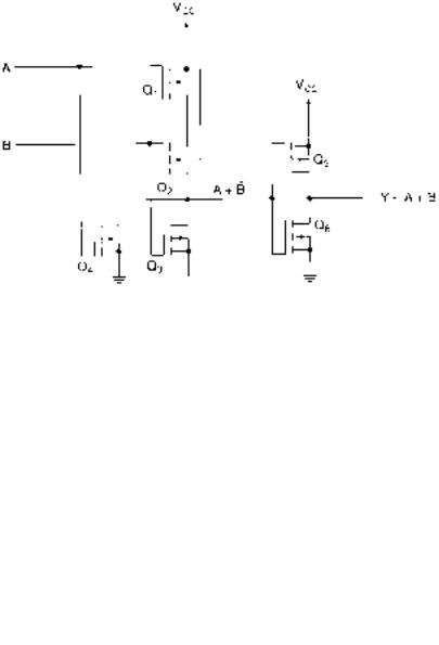
When either input is HIGH, the output is LOW. This function is implemented by two parallel n-channel MOSFETs. Both inputs must be LOW to make the output HIGH, which implies a series connection of two p-channel transistors. The complete NOR gate circuit is shown in Figure 11.55. (Note that the substrate of Q2 is connected directly to VCC to ensure that it has its own bias voltage.)
FIGURE 11.55
CMOS NOR Gate
As was the case with the NAND circuit, transistors Q1 and Q4 form a complementary MOSFET pair. Transistors Q2 and Q3 form the second pair.
When both inputs are LOW, both p-channel transistors are ON. This creates a lowimpedance path from VCC to output Y. The n-channel transistors, Q3 and Q4, are both OFF. This isolates the output from ground. Output Y is HIGH. Table 11.12 shows the MOSFET states under this condition.
Table 11.12 Partial CMOS NOR Function
and Truth Table
A B |
Q1 |
Q2 |
Q4 |
Q4 |
Y |
|
|
|
|
|
|
0 0 |
ON |
ON |
OFF |
OFF |
1 |
|
|
|
|
|
|
If either input is HIGH, one or both of the p-channel transistors will turn OFF. This action breaks the path from VCC to output Y. The complementary n-channel transistor will turn ON. This creates a low-impedance path from output Y to ground. Output Y is LOW. Table 11.13 summarizes the possible input conditions and MOSFET states when the NOR output is LOW.
Table 11.13 Partial CMOS NOR Function
and Truth Table
A B |
Q1 |
Q2 |
Q3 |
Q4 |
Y |
|
|
|
|
|
|
|
|
0 |
1 |
ON |
OFF |
ON |
OFF |
0 |
1 |
0 |
OFF |
ON |
OFF |
ON |
0 |
1 |
1 |
OFF |
OFF |
ON |
ON |
0 |
|
|
|
|
|
|
|