

Dueck R.Digital design with CPLD applications and VHDL.2000
.pdf530 C H A P T E R 1 1 • Logic Gate Circuitry
FIGURE 11.33
Circuit Model for Pull-up Resistor Calculation
N O T E
The main rule in resistor selection is to keep the sum of currents into the open-col- lector output to less than the maximum rated value of IOL.
IOL IR nIIL
IR (VCC VOL /Rext
EXAMPLE 11.15 |
Calculate the minimum value of the pull-up resistor for a 74LS05 inverter if the circuit dri- |
|
ves ten 74LS00 NAND gate inputs. |
|
Solution |
From 74LS00 specs: |
IIL 0.4 mA |
For 10 gates: |
nIIL 10IIL 4 mA |
From 74LS05 specs: |
IOL 8 mA |
|
IR IOL nIIL |
|
8 mA 4 mA |
|
4 mA |
For IOL 8 mA, VOL 0.5 V |
|
Rext (VCC VOL)/IR
(5 V 0.5 V)/4 mA
4.5 V/4 mA 1.125 k
Use a 1.2-k or 1.5-k standard value resistor.
SECTION 11.7B REVIEW PROBLEM
11.8Calculate the minimum value of pull-up resistor required for a 74LS05 inverter if it drives one input of a 74LS00 NAND gate. What is the minimum standard value of this resistor?

11.7 • Internal Circuitry of TTL Gates |
531 |
Totem Pole Outputs
K E Y T E R M S
Totem pole output A type of TTL output with a HIGH and a LOW output transistor, only one of which is active at any time.
Phase splitter A transistor in a TTL circuit that ensures that the LOWand HIGH-state output transistors of a totem pole output are always in opposite phase (i.e., one ON, one OFF).
Figure 11.34 shows one gate of a 7400 quadruple 2-input NAND with totem pole outputs. The circuit is the same as that for a 7401 open-collector NAND except for a transistor, resistor, and diode, which make up the HIGH-state output circuitry of the NAND gate.
FIGURE 11.34
NAND Gate With Totem Pole Output
The totem pole output, shown in Figure 11.34b, has separate transistors to switch the output to the HIGH state (Q4) and the LOW state (Q3). These transistors are switched by Q2, the phase splitter. Only one of them is ON at a time; the currents IOH and IOL never flow simultaneously.
The portion of the circuit consisting of Q4, D3, and the 130resistor replaces the external pull-up resistor required by the open-collector TTL output. Since the HIGH state is switched by its own transistor, we say that the circuit has an active pull-up.
The main advantage of the totem pole output over the open collector is that it can change states faster. The external pull-up resistance needed in an open-collector circuit slows down the output switching by contributing to the RC time constant of the output. The HIGH-state transistor circuit, with its relatively low output impedance, reduces this time constant and thus improves switching speed.

532 C H A P T E R 1 1 • Logic Gate Circuitry
FIGURE 11.35
NAND Gate Operation
Figure 11.35 shows the operation of the 7400 NAND gate for HIGH and LOW input conditions.
HIGH Input. When both inputs are HIGH, there is no low-impedance base-emitter current path in Q1. The base-collector junction of Q1 acts as a forward-biased diode. Base current flows in Q2, saturating the transistor. Sufficient current flows to Q3 to saturate it. Y is connected to ground, via the collector-emitter path of Q3. The output is LOW.
LOW Input. Figure 11.35b shows input B of a 7400 NAND gate pulled LOW. The circuit operates the same way if A or both A and B are LOW.
In this condition, a low-impedance path to ground is established through one of the base-emitter junctions of Q1. This pulls the base of Q2 LOW, causing it to be in cutoff

11.7 • Internal Circuitry of TTL Gates |
533 |
mode. No current flows through the collector-emitter path of Q2, so no base current flows in Q3; it is also cut off.
Current flows through the 1.6-k resistor to the base of Q4, turning it ON. This connects the output, via Q4, D3, and the 130resistor, to VCC. The output is HIGH.
Q4 will not turn ON when Q3 is ON. We can find out why by calculating VBE4 VD3. For Q4 to conduct, two pn junctions (D3 and the base-emitter junction of Q4) must be for-
ward-biased. Thus, (VBE4 VD3) must be greater than 0.6 V 0.6 V 1.2 V.
VBE4 VD3 VB4 VCE3
We can calculate VB4 by adding up voltage drops, as follows:
VB4 VCE2 VBE3 0.2 V 0.7 V 0.9 V
Q3 is saturated, thus:
VCE3 0.2 V
The difference between these voltages is:
VB4 VCE3 0.9 V 0.2 V 0.7 V
This is insufficient to forward-bias BE4 and D3. Q4 stays OFF.
N O T E
Without D3 in the circuit,
VBE4 (VCE2 VBE3) VCE3
(0.2 V 0.7 V) 0.2 V
0.7 V
This is sufficient to saturate Q4, even when Q3 is ON. The diode is therefore necessary to keep Q4 OFF when Q3 is ON.
Switching Noise
K E Y T E R M
Storage time Time required to transport stored charge away from the base region
of a bipolar transistor before it can turn off.
A totem pole output is an inherently noisy circuit. Noise is generated on the supply voltage line when the output switches from LOW to HIGH.
When the output is in a steady HIGH or LOW state, Q3 and Q4 are always in opposite phase. The design of the totem pole output is such that when Q3 is ON, it is saturated, but when Q4 is ON, it operates in the transistor’s active, or linear, region.
A saturated transistor takes longer to shut off than an unsaturated one due to storage time, the time required to transport stored charge away from the base region of the transistor. Thus, Q3 takes longer to turn off than Q4.
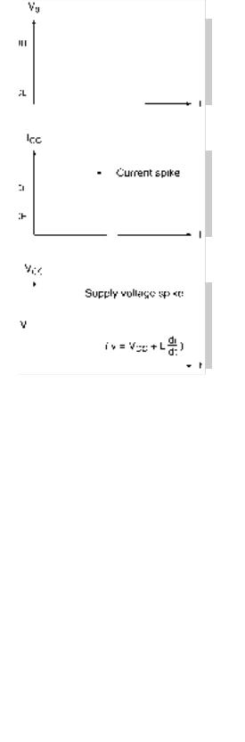
When a totem pole output is LOW, Q3 is ON and Q4 is OFF. When the output changes state, Q4 turns ON before Q3 can turn OFF, due to the storage time of Q3. For a few nanoseconds, both transistors are ON. This condition momentarily shorts VCC to ground, causing a surge of supply current, as shown in Figure 11.36.
The inductance of the power line produces a corresponding spike proportional to the instantaneous rate of change of the supply current (v L di/dt, where L is the power line inductance and di/dt is the instantaneous rate of change of supply current).
These spikes on the supply voltage line can cause real problems, especially in synchronous circuits. They often cause erroneous switching that is nearly impossible to troubleshoot. The best cure for such problems is prevention.
534 C H A P T E R 1 1 • Logic Gate Circuitry
FIGURE 11.36
Spikes on Power Line During LOW-to-HIGH Transition of Totem Pole Output
Figure 11.37 shows the addition of a decoupling capacitor to a totem pole output to eliminate switching spikes. A low-inductance capacitor of about 0.1 F is placed between the VCC and ground pins of the chip to be decoupled. This capacitor offsets the power line inductance and acts as a low-impedance path to ground for high-frequency noise (i.e., spikes). Since a capacitor is an open circuit for low frequencies, the normal DC supply voltage is not shorted out.
FIGURE 11.37
Decoupling the Power Supply


536 C H A P T E R 1 1 • Logic Gate Circuitry
FIGURE 11.40
Totem Poles Connected Together
SECTION 11.7C REVIEW PROBLEM
11.9 A totem pole output is likely to be damaged when shorted to ground. Why?
Tristate Gates
K E Y T E R M
Tristate output An output having three possible states: logic HIGH and LOW,
and a high-impedance state, in which the output acts as an open circuit.
Figure 11.41 shows the circuits of two TTL inverters with tristate outputs. In addition to the usual binary states of HIGH and LOW, the output of the tristate inverter can also be in a “high-impedance” (Hi-Z) state. This state occurs when both Q3 and Q4 are OFF. The electrical effect is to produce an open circuit at the output, which is neither HIGH nor LOW.
The output of a tristate gate combines advantages of a totem pole output and an opencollector output. Like the totem pole output, it has an active pull-up with lower output impedance and faster switching than an open collector. Like the open collector, we can connect several outputs together, provided only one output is active at a time.
Input G, the “gating” or “enable” input, controls the gate. When G is active, the gate acts as an ordinary inverter. When inactive, the gate is in the high-impedance state. Table 11.6 summarizes the operation of the tristate inverters in Figure 11.41.
The tristate inverter in Figure 11.41a is enabled by a HIGH at the G input. The circuit is the same as a 7400 NAND gate with two exceptions: (1) an extra diode goes from the base of Q4 to G, and (2) G connects directly to one of the emitters of Q1.
When G 0, Q1 acts as though there was a LOW at a NAND gate input. In a 7400 NAND circuit, this causes Q2 and Q3 to be in cutoff mode.
Due to the opposite states of the emitter and collector in Q2, Q4 would normally be ON. Instead, the LOW at G pulls the base of Q4 LOW through the extra diode. Thus, both Q3 and Q4 are OFF.
When G 1, the G emitter of Q1 acts like a HIGH NAND input. By the enable/ inhibit rules of a NAND gate, Y A. The additional diode prevents the HIGH at G from activating Q4.
The circuit in Figure 11.41b works the same way, except for the opposite sense of the activating input. This opposite active level is achieved by using an open-collector inverter, consisting of Q5, Q6, and Q7, at input G.

11.7 • Internal Circuitry of TTL Gates |
537 |
FIGURE 11.41
Tristate Inverters
Table 11.6 Truth Tables of Tristate
Inverters
G |
A |
Y |
|
A |
Y |
G |
|||||
|
|
|
|
|
|
0 |
0 |
Hi-Z |
0 |
0 |
1 |
0 |
1 |
Hi-Z |
0 |
1 |
0 |
1 |
0 |
1 |
1 |
0 |
Hi-Z |
1 |
1 |
0 |
1 |
1 |
Hi-Z |
|
|
|
|
|
|

538 C H A P T E R 1 1 • Logic Gate Circuitry
SECTION 11.7D REVIEW PROBLEM
11.10Why is the diode from the base of Q4 necessary in the tristate inverters in Figure 11.41?
Other Basic TTL Gates
Other TTL gates are similar to the NAND and inverter gates we have already examined. A significant variation is the OR/NOR circuit, which has a different input configuration than the AND/NAND/inverter type gates.
7402 NOR Gate
Figure 11.42 shows one gate of a 7402 quadruple 2-input NOR gate package. The difference between this gate and the 7400 NAND gate is the structure of the inputs. The NOR gate does not use the multiple-emitter transistor, but rather an individual transistor (Q1 or Q2) for each input. There are two phase splitters (Q3 and Q4), which are paralleled, emitter- to-emitter and collector-to-collector.
FIGURE 11.42
7402 NOR Gate Circuit
If either Q3 or Q4 is enabled by a HIGH at its corresponding input, it will turn on Q5, making the output LOW.
If both gate inputs are LOW, both Q3 and Q4 are in cutoff mode, and so is Q5. The output is HIGH through Q6.
Table 11.7 shows the truth table and the states of the transistors for this gate. It is not strictly correct to refer to Q1 and Q2 as being ON or OFF, since there is current flowing in these transistors regardless of whether the inputs are HIGH or LOW. Let us define the ON
