

Dueck R.Digital design with CPLD applications and VHDL.2000
.pdf520 |
C H A P T E R |
1 1 • Logic Gate Circuitry |
|
|
|
EXAMPLE 11.13 |
Figure 11.18 shows an NPN bipolar transistor connected in a common-emitter configura- |
|
|
|
tion. With the right choice of input voltages, this circuit acts as a digital inverter. |
FIGURE 11.18
Example 11.13
Transistor as Inverter
Analyze the circuit to show that it acts as an inverter if a logic HIGH is defined as3 V and a logic LOW is defined as 0.5 V. Assume that b 100, and assume that VBE 0.7 V and VCE 0.2 V in saturation.
Solution We will analyze the circuit with two input voltages: 3 V (logic HIGH) and 0.5
V (logic LOW). These two conditions are shown in Figure 11.19.
FIGURE 11.19
Example 11.13
Voltage and Current Analysis of Inverter
High input. We must prove that VI 3 V is sufficient to saturate the transistor. Let us assume that this is true and find out if calculations confirm our assumption.
Figure 11.19a shows the circuit with VI 3 V. By Kirchhoff’s voltage law (KVL):
VI IBRB VBE, or
IB (VI VBE)/RB
If we assume that IB is sufficient to saturate the transistor, then:
IB (3 V 0.7 V)/22 k
105 A
bIB (100)(105 A) 10.5 mA
Collector current won’t increase beyond its saturated value, even if base current increases. Therefore, if the transistor is saturated, bIB will be larger than the current actually flowing in the collector-emitter path.

11.7 • Internal Circuitry of TTL Gates |
521 |
In saturation, the collector current can be calculated by KVL:
VCC IC RC VCE, or
IC (VCC VCE)/RC
IC (5 V 0.2 V)/470
10.2 mA
Since bIB IC, the transistor is saturated. Thus, an input voltage of 3 V will produce sufficient base current to saturate the transistor. The output is given by VO VCE 0.2 V, which is within the defined range of a logic LOW.
LOW input. Figure 11.19b shows the circuit with VI 0.5 V. By KVL:
VI IB RB VBE
VBE 0.5 V IB RB
Since VBE must be 0.6 V, the transistor is in cutoff mode. Thus, in the collector circuit:
VCC IC RC VCE
5 V (0)(470 ) VCE
VO VCE 5 V (logic HIGH)
Table 11.6 summarizes the operation of the circuit as an inverter.
Table 11.6 Input and Output of Single-Transistor
Inverter
|
Input |
|
Output |
|
|
|
|
VI |
Logic Level |
VO |
Logic Level |
|
|
|
|
0.5 V |
LOW |
5 V |
HIGH |
3 V |
HIGH |
0.2 V |
LOW |
|
|
|
|
TTL Open-Collector Inverter and NAND Gate
K E Y T E R M
Open-collector output A TTL output where the collector of the LOW-state output transistor is brought out directly to the output pin. There is no built-in HIGH-
state output circuitry, which allows two or more open-collector outputs to be connected without possible damage.
N O T E
The TTL gates (7405, 7401, 7404, 7400, and 7402) used in the following sections to illustrate TTL circuit principles are no longer in general use. They are from the original (“standard”) TTL family, which has been superceded by faster and more efficient devices. However, the standard TTL devices are easier to understand than devices from the newer TTL subfamilies, since their circuit structure is simpler. The operating principles are similar in both the standard and newer families, so we will use the standard devices to illustrate the general principles of TTL operation.
Figure 11.20 shows the circuit of the simplest TTL gate: a 7405 inverter with open-collector outputs. This circuit performs the same function as the single-transistor inverter we examined in Example 11.13. These circuits differ most obviously in their input circuitry. The inverter circuit in Example 11.13 has a resistor as its input; the 7405 inverter has a transistor,

522 C H A P T E R 1 1 • Logic Gate Circuitry
FIGURE 11.20
Open-Collector Inverter (7405)
Q1, as its input. The input transistor allows faster switching of input states. This configuration is common to all standard TTL gates and will be examined in detail later in this section.
The logic function of the 7405 is performed by transistors Q2 and Q3. Output transistor Q3 is switched ON and OFF by current flowing in the collector-emitter path of Q2. When Q3 is ON, Y is LOW.
However, when Q3 is OFF, Y is floating. There is a high impedance between Y and ground, so the output is not LOW. But there is no connection to VCC to make the output HIGH. In this condition, Y is neither HIGH nor LOW.
To enable the output to produce a HIGH state, we need to add an external pull-up resistor. The value of this resistor depends on the current sinking capability of Q3, specified in the data sheet as IOL. We will do such calculations in a later example.
TTL Inputs
Transistor Q1 and diode D1 make up the input circuit of the TTL inverter of Figure 11.20. The diode protects the input against small negative voltages. If the input goes more negative than about 0.7 V, the diode will conduct, effectively short-circuiting the input to ground plus one diode drop. This clamps the input to 0.7 V. D1 has no logic function.
Q1 can be treated as two back-to-back diodes, as shown in Figure 11.21. Figure 11.22 shows how the input responds to logic HIGH and LOW voltages.
LOW Input. When a TTL input is made LOW, the base-emitter junction of Q1 acts as a forward-biased diode, creating a current path from VCC to ground via the input pin. This

11.7 • Internal Circuitry of TTL Gates |
523 |
FIGURE 11.21
Diode Equivalent of TTL Input
Transistor
FIGURE 11.22
HIGH and LOW Inputs at a
TTL Gate
current makes up the majority of current IIL, which has a maximum value of 1.6 mA in standard TTL (0.4mA in LSTTL).
At the moment the input is made LOW, the transistor action of Q1 transports charge away from the base of Q2, pulling it LOW and keeping it in cutoff mode. This current dies out when the base charge of Q2 has been depleted, shortly after the LOW is applied to the input pin. The diode formed by the base-collector junction of Q1 does not carry sufficient current to turn on Q2, since the base-emitter path is of much lower impedance.
HIGH Input. A HIGH at a TTL input reverse-biases the base-emitter junction of Q1. Only a small leakage current, IIH, flows. The maximum value of IIH is 40 A for standard TTL (20 A for LSTTL).
Since the low-impedance current path to the input pin has not been established, current flows to the base of Q2 via the forward-biased base-collector junction of Q1. This current is sufficient to saturate Q2.
Open (Floating) TTL Input. An open-circuit TTL input acts as a logic HIGH, as illustrated by Figure 11.23. A TTL input relies on a logic LOW to establish a low-impedance current path from VCC to the input pin. If the input is open, this LOW is not present and current flows in the base-collector junction of the transistor, by default. This is the same current that flows under the HIGH-input condition.
This HIGH is not stable; it can be converted to logic LOW by induced noise at the input pin. To avoid this uncertainty, an unused input should always be wired to a logic HIGH or LOW state.
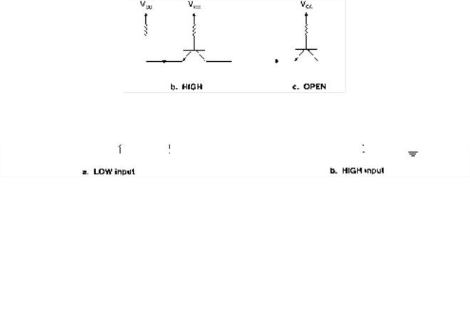
524 C H A P T E R 1 1 • Logic Gate Circuitry
FIGURE 11.23
LOW, HIGH, and Open
TTL Inputs
TTL Open-Collector Inverter
Figure 11.24 shows the operation of the 7405 open-collector inverter.
FIGURE 11.24
7405 Operation
LOW Input. As was described above, a LOW input establishes a low-impedance path to ground, which draws current through the base-emitter junction of Q1. This action also prevents base current from flowing in transistor Q2, causing it to be in cutoff mode and mak-
ing IC2 0.
Since IB3 is derived from IC2, IB3 0 and Q3 is cut off, making a high-impedance path between the collector and emitter of Q3. As was the case with the single-transistor inverter in Example 11.13, when IC3 0, then VO VCE VCC. (Since no current flows through the pull-up resistor, the voltage must be the same at both ends.) Output Y is HIGH.
HIGH Input. When input A is HIGH, the base-emitter junction of Q1 does not have sufficient voltage across it to be forward-biased. Current flows through the base-collector junction of Q1, saturating Q2.
Since Q2 is ON, current flows to the Q2 emitter and splits through the 1-k resistor and the base of Q3. The output transistor, Q3, turns ON, establishing a low-impedance current path from output Y to ground. Current is limited by the external pull-up resistor, which
must be chosen to keep IOL at or under its rated value of 16 mA. VCE3 is about 0.2 V to 0.4 V. Output Y is LOW.
TTL Open-Collector NAND
Figure 11.25 shows one gate of a 7401 quadruple 2-input NAND gate with open-collector outputs. The circuit is the same as that of the 7405 inverter, except that the input transistor has a second emitter. Multiple-emitter transistors of this type are common in TTL circuits and can be modeled by the diode equivalent in Figure 11.25b. Figure 11.26 shows the response of the multiple-emitter input transistor to various combinations of logic levels.

11.7 • Internal Circuitry of TTL Gates |
525 |
FIGURE 11.25
TTL NAND with Open Collector Output
FIGURE 11.26
Input Response of Multiple-Emitter Transistor
If both inputs are LOW, the NAND acts exactly the same as the 7405 inverter with a LOW input. (A low-impedance path is created through a base-emitter junction.) Output Y is HIGH, provided an external pull-up resistor is connected to output. A partial truth table for this condition is:
A B Y
0 0 1
If one input is LOW, the input acts the same as the inverter with a LOW input. The lowimpedance current path through the one grounded emitter prevents sufficient basecollector current from flowing to forward-bias that junction. Output Y is HIGH if a pull-up resistor is connected to the output. A partial truth table is as follows:
A B Y
0 1 1
1 0 1

526 C H A P T E R 1 1 • Logic Gate Circuitry
If both inputs are HIGH, the NAND circuit acts like the 7405 when its input is HIGH. (There is no base-emitter current path. A collector-emitter path is established by default.) Output Y is LOW. This condition can be represented by:
A B Y
1 1 0
Combining all these conditions, we get the standard NAND truth table:
A B Y
0 0 1
0 1 1
1 0 1
1 1 0
N O T E
If one or more emitters of a TTL multiple-emitter input transistor is LOW, the input is a LOW equivalent. All emitters must be HIGH to make the transistor input a HIGH equivalent.
These statements lead to the familiar NAND-gate descriptive sentences, illustrated by the gate symbols in Figure 11.27.
a.At least one input LOW makes the output HIGH.
b.Both inputs HIGH make the output LOW.
FIGURE 11.27
DeMorgan Equivalent Forms of a NAND Gate
SECTION 11.7A REVIEW PROBLEM
11.7What are the two main functions of the pull-up resistor on the output of an opencollector gate?
Open-Collector Applications
K E Y T E R M
Wired-AND A connection where open-collector outputs of logic gates are wired
together. The logical effect is the ANDing of connected functions.
A more common TTL output than the open collector is the totem pole output, which we will study later in this chapter. The totem pole output has its own internal pull-up circuit for HIGH outputs.

11.7 • Internal Circuitry of TTL Gates |
527 |
Gates with totem pole outputs cannot be used in all digital circuits. For example, opencollector gates are required when several outputs must be tied together, a connection called wired-AND. Totem pole outputs would be damaged by such a connection, since there is the possibility of conflict between an output HIGH and LOW state.
Open-collector outputs can also be used for applications requiring high current drive and for interfacing to circuits having supply voltages other than TTL levels.
A special symbol defined by IEEE/ANSI Standard 91-1984, an underlined square diamond, is shown in Figure 11.28. This symbol is added to a logic gate symbol to indicate that it has an open-collector output. Other symbols, such as a star (*), a dot (●), or the initials OC are also used.
Wired-AND
N O T E
A wired-AND connection combines the outputs of the connected gates in an AND function.
FIGURE 11.28 |
FIGURE 11.29 |
Open-Collector Symbols Shown |
Three Inverters in a Wired-AND |
for a NAND Gate (e.g., 7401) |
Connection |
Figure 11.29 shows three open-collector inverters connected in a wired-AND configuration. The output transistors of the inverters are shown in Figure 11.30, with different possible ON and OFF states. The only way output Y can remain HIGH is if all the transistors are in their OFF states, as in Figure 11.30c. This can happen only if the outputs of the inverters are all HIGH. This is the same as saying the outputs are ANDed together at Y.
The Boolean expression for Y is:
Y A B C
A B C
By DeMorgan’s theorem, the wired-AND connection of inverter outputs is equivalent to a NOR function. Because of this DeMorgan equivalence, the connection is sometimes called “wired-OR.”
Figure 11.31 shows three NAND gates in a wired-AND connection. Since the output functions are ANDed, the Boolean expression for Y is:
Y AB CD EF
AB CD EF

