

Dueck R.Digital design with CPLD applications and VHDL.2000
.pdf450 C H A P T E R 9 • Counters and Shift Registers
Count sequence The specific series of output states through which a counter progresses.
Counter A sequential digital circuit whose output progresses in a predictable repeating pattern, advancing by one state for each clock pulse.
Count-sequence table A list of counter states in the order of the count sequence.
Dataflow design A VHDL design technique that uses Boolean equations to define relationships between inputs and outputs.
DOWN counter A counter with a descending sequence.
Excitation table A table showing the required input conditions for every possible transition of a flip-flop output.
Full-sequence counter A counter whose modulus is the same as its maximum modulus (m 2n for an n-bit counter).
GENERIC A clause in the entity declaration of a VHDL component that lists the parameters that can be specified when the component is instantiated.
Johnson counter A serial shift register with complemented feedback from the output of the last flip-flop to the input of the first. Also called a twisted ring counter
Left shift A movement of data from the right to the left in a shift register. (Left is defined in MAX PLUS II as toward the MSB.)
Maximum modulus (mmax) The largest number of counter states that can be represented by n bits (mmax 2n)
Memory section A set of flip-flops in a synchronous circuit that hold its present state.
Modulo-n (or mod-n) counter A counter with a modulus of n.
Modulus The number of states through which a counter sequences before repeating.
Next state The desired future state of flip-flop outputs in a synchronous sequential circuit after the next clock pulse is applied.
Parallel load A function that allows simultaneous loading of binary values into all flip-flops of a synchronous circuit. Parallel loading can be synchronous or asynchronous.
Parallel-load shift register A shift register that can be preset to any value by directly loading a binary number into its internal flip-flops.
Parallel transfer Movement of data into all flip-flops of a shift register at the same time.
Present state The current state of flip-flop outputs in a synchronous sequential circuit.
UP counter A counter with an ascending sequence.
P R O B L E M S
Problem numbers set in color indicate more difficult problems; those with underlines indicate most difficult problems.
9.1Basic Concepts of Digital Counters
9.1A parking lot at a football stadium is monitored before a game to determine whether or not there is available space for more cars. When a car enters the lot, the driver takes a ticket from a dispenser which also produces a pulse for each ticket taken.
The parking lot has space for 4095 cars. Draw a block
Presettable counter A counter with a parallel load function.
Recycle To make a transition from the last state of the count sequence to the first state.
Right shift A movement of data from the left to the right in a shift register. (Right is defined in MAX PLUS II as toward the LSB.)
Ring counter A serial shift register with feedback from the output of the last flip-flop to the input of the first.
Ripple carry out or ripple clock out (RCO) An output that produces one pulse with the same period as the clock upon terminal count.
Rotation Serial shifting of data with the output(s) of the last flip-flop connected to the synchronous input(s) of the first flipflop. The result is continuous circulation of the same data.
Serial shifting Movement of data from one end of a shift register to the other at a rate of one bit per clock pulse.
Shift register A synchronous sequential circuit that will store and move n-bit data, either serially or in parallel, in n flip-flops.
SRGn Symbol for an n-bit shift register (e.g., SRG4 indicates a 4-bit shift register).
State diagram A diagram showing the progression of states of a sequential circuit.
State machine A synchronous sequential circuit.
Status lines Signals that communicate the present state of a synchronous circuit from its memory section to its control section.
Structural design A VHDL design technique that connects predesigned components using internal signals.
Synchronous counter A counter whose flip-flops are all clocked by the same source and thus change in synchronization with each other.
Terminal count The last state in a count sequence before the sequence repeats (e.g., 1111 is the terminal count of a 4-bit binary UP counter; 0000 is the terminal count of a 4-bit binary DOWN counter).
Truncated-sequence counter A counter whose modulus is less than its maximum modulus (m 2n for an n-bit counter)
Universal shift register A shift register that can operate with any combination of serial and parallel inputs and outputs (i.e., serial in/serial out, serial in/parallel out, parallel in/serial out, parallel in/parallel out). A universal shift register is often bidirectional, as well.
diagram which shows how you can use a digital counter to light a LOT FULL sign after 4095 cars have entered. (Assume no cars leave the lot until after the game, so you don’t need to keep track of cars leaving the lot.) How many bits should the counter have?
9.2Figure 9.86 shows a mod-16 which controls the operation of two digital sequential circuits, labeled Circuit 1 and Circuit 2. Circuit 1 is positive edge-triggered and
clocked by counter output Q1. Circuit 2 is negative edgetriggered and clocked by Q3. (Q3 is the MSB output of

CTR DIV 16
CLK
CLK
Q3 Q2 Q1 Q0
 Circuit 1
 Circuit 2
FIGURE 9.86
Problem 9.2
Mod-16 Counter Driving Two Sequential Circuits
the counter.)
a.Draw the timing diagram for one complete cycle of the circuit operation. Draw arrows on the active edges of the waveforms that activate Circuit 1 and Circuit 2.
b.State how many times Circuit 1 is clocked for each time that Circuit 2 is clocked.
9.3Draw the timing diagram for one complete cycle of a
mod-8 counter, including waveforms for CLK, Q0, Q1, and Q2, where Q0 is the LSB.
9.4How many bits are required to make a counter with a modulus of 64? Why? What is the maximum count of such a counter?
9.5a. Draw the state diagram of a mod-10 UP counter.
b.Use the state diagram drawn in part a to answer the following questions:
FIGURE 9.87
Problem 9.14
Synchronous Counter
Problems 451
i.The counter is at state 0111. What is the count after 7 clock pulses are applied?
ii.After 5 clock pulses, the counter output is at 0001. What was the counter state prior to the clock pulses?
iii.The counter output is at 1000 after 15 clock pulses. What was the original output state?
9.6What is the maximum modulus of a 6-bit counter? A 7- bit? 8-bit?
9.7Draw the count sequence table and timing diagram of a mod-10 UP counter.
9.8Draw the state diagram, count sequence table, and timing diagram of a mod-10 DOWN counter.
9.9A mod-16 counter is clocked by a waveform having a frequency of 48 kHz. What is the frequency of each of the waveforms at Q0, Q1, Q2, and Q3?
9.10 A mod-10 counter is clocked by a waveform having a frequency of 48 kHz. What is the frequency of the Q3 output waveform? The Q0 waveform? Why is it difficult to determine the frequencies of Q1 and Q2?
9.2Synchronous Counters
9.11Draw the circuit for a synchronous mod-16 UP counter made from negative edge-triggered JK flip-flops.
9.12Write the Boolean equations required to extend the counter drawn in Problem 9.11 to a mod-64 counter.
9.13Write the J and K equations for the MSB of a synchronous mod-256 (8-bit) UP counter.
9.14Analyze the operation of the synchronous counter in Figure 9.87 by drawing a state table showing all transitions, including unused states. Use this state table to draw a state diagram and a timing diagram. What is the counter’s modulus?
9.15a. Write the equations for the J and K inputs of each flip-
452 C H A P T E R 9 • Counters and Shift Registers
FIGURE 9.88
Problem 9.15
Synchronous Counter
FIGURE 9.89
Problem 9.16
Counter
flop of the synchronous counter represented in Figure 9.88.
b.Assume that Q3Q2Q1Q0 1010 at some point in the count sequence. Use the equations from part a to predict the circuit outputs after each of three clock pulses.
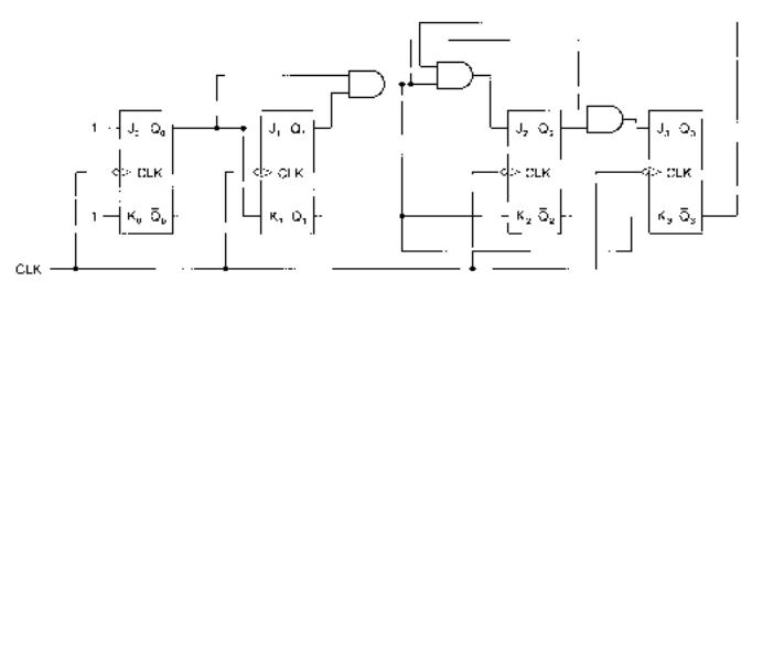
9.16Analyze the operation of the counter shown in Figure 9.89. Predict the count sequence by determining the J and K inputs and resulting transitions for each counter output state. Draw the state diagram and the timing diagram. Assume that all flip-flop outputs are initially 0.
9.3Design of Synchronous Counters
9.17Draw the timing diagram and state diagram of a synchronous mod-10 counter with a positive edge-triggered clock.
9.18Design a synchronous mod-10 counter, using positive edge-triggered JK flip-flops. Check that unused states properly enter the main sequence. Draw a state diagram showing the unused states.
9.19Design a synchronous mod-10 counter, using positive edge-triggered D flip-flops. Check that unused states properly enter the main sequence. Draw a state diagram showing the unused states.
9.20Design a synchronous 3-bit binary counter using T flipflops.
9.21Table 9.20 shows the count sequence for a biquinary sequence counter. The sequence has ten states, but does not progress in binary order. The advantage of the sequence is that its most significant bit has a divide-by-10 ratio, relative to a clock input, and a 50% duty cycle. Design the

Table 9.20 Biquinary
Sequence
Q3Q2Q1Q0
0000
0001
0010
0011
0100
1000
1001
1010
1011
1100
synchronous counter circuit for this sequence, using D flip-flops. Hint: When making the state table, list all present states in binary order. The next states will not be in binary order.
9.4Programming Binary Counters in VHDL
9.22Write the VHDL code for a behavioral description of a 6- bit binary counter with asynchronous clear.
9.23Create a simulation file in MAX PLUS II to verify the operation of the counter in Problem 9.22. (Use a 40 ns clock, which approximates the clock period of the oscillator on the Altera UP-1 board.) Note: To make a useful simulation, you must include the recycle point, which may be beyond the default end time of the simulation (1 ms). To change the end time, select End Time from the MAX PLUS II File menu in the Simulator menu. To change the clock period, select Grid Size from the MAX PLUS II Options menu in the Simulator window. The default clock period is two grid spaces.
9.24Write a VHDL file that instantiates a counter from the Library of Parameterized Modules to make a 12-bit binary counter. Create a MAX PLUS II simulation to verify the operation of the counter. (Refer to the note after Problem 9.23.)
9.5Control Options for Synchronous Counters
9.25Briefly explain the difference between asynchronous and synchronous parallel load in a synchronous counter. Draw a partial timing diagram that illustrates both functions for a 4-bit counter.
9.26Refer to the 4-bit counter of Figure 9.26 (p. 391). The graphic design files for the counter are found on the CD accompanying this text as 4bit_sl.gdf and sl_count.gdf in the folder drive:\Student_Files\Chapter09. Copy these files to a new folder and use the MAX PLUS II graphic editor to expand the counter of Figure 9.26 to a 5-bit counter with synchronous load and asynchronous reset. Save and compile the file to make sure that there are no design errors.
9.27Create a MAX PLUS II simulation to verify the functions of the counter in Problem 9.26. The simulation must include the recycle point of the counter and show that the
Problems 453
load is really synchronous and that the reset is really asynchronous.
9.28 Refer to the 4-bit counter of Figure 9.33 (p. 396). The graphic design files for the counter are found on the accompanying CD as 4bit_sle.gdf and sl_count.gdf in the folder drive:\Student Files\Chapter09. Copy these files to a new folder and modify the synchronous count element sl_count.gdf so that it implements an active-HIGH synchronous load and an active-LOW synchronous clear function, as well as the binary count function. Create a default symbol for the new element and substitute it in 4bit_sle.gdf for the existing counter elements sl_count. The load function should have priority over count enable, and clear (reset) should have priority over both. Save and compile the new file. Hints: (1) The clear function makes Q 0 after a clock pulse. (2) Q follows D.
9.29Create a MAX PLUS II simulation to verify the functions of the counter in Problem 9.28. The simulation must include the recycle point of the counter and show that the load and clear really are synchronous and that load has priority over count enable and clear has priority over both.
9.30Derive the Boolean equations for the synchronous DOWN-counter in Figure 9.35.
9.31Write the Boolean equations for the count logic of the 4- bit bidirectional counter in Figure 9.38. Briefly explain how the logic works.
9.32Draw a MAX PLUS II Graphic Design File for a bidirectional counter, using T flip-flops. Create a simulation of the counter to verify its function
9.33Use MAX PLUS II to create a synchronous bidirectional counter with synchronous load, asynchronous reset, and count enable. The count enable should not affect the operation of the load and reset functions. The functions should have the following priority: (1) clear; (2) load; and
(3) count. Create a MAX PLUS II simulation to verify the operation of your design.
9.6 Programming Presettable and Bidirectional
Counters in VHDL
9.34Write the VHDL code for a counter that uses a behavioral description of the following functions: 12-bit binary UP count; active-LOW asynchronous clear, active-LOW synchronous load, active-LOW count enable, terminal count decoder. The clear function should have the highest priority, followed by load, then count enable. Create a simulation in MAX PLUS II that verifies the functions of this counter.
9.35Write theVHDL code for a behavioral description of a bidirectional counter with a modulus of 24. The counter should also have an active-LOW synchronous clear function that has priority over the count. Create a MAX PLUS II simulation file to verify the counter operation.
9.36Write the VHDL code for a 4-bit counter with two decoding outputs called eq8 and eq12. Out eq8 goes HIGH when the count equals 8 and eq12 goes HIGH when the count equals 12 (decimal). The counter should also have an active-LOW asynchronous clear function that has pri-

454 C H A P T E R 9 • Counters and Shift Registers
FIGURE 9.90
Problem 9.44
Timing Diagram
ority over the count. Create a MAX PLUS II simulation file to verify the counter operation.
9.37Modify the VHDL code in Example 9.10 (p. 412) so that the counter synchronously sets to all 1s ( 4095), rather than to 2047. Do not use SVALUE 4095. Create a simulation in MAX PLUS II that verifies the operation of the counter. State the main difference between the code for Example 9.10 and the solution to this problem.
9.38Use a counter from the Library of Parameterized Modules to implement the counter described in Problem 9.35. Create a MAX PLUS II simulation file to verify the operation of the counter.
9.39Write a VHDL file that instantiates an 8-bit LPM count with synchronous load and clear, count enable, and directional control. Also include a terminal count decoder. (The LPM counter has no port for the terminal count function, so it must be done separately.) Create a MAX PLUS II simulation to verify the operation of the counter.
9.7Shift Registers
9.40Use the MAX PLUS II Graphic Editor to draw the circuit of a serial shift register constructed from JK flipflops. Create a simulation to verify the operation of the shift register.
9.41Use the MAX PLUS II Graphic Editor to create the logic diagram of the 4-bit serial shift register based on JK flip-flops that shifts left, rather than right. Create a simulation to verify the operation of the shift register.
9.42The following bits are applied in sequence to the input of a 6-bit serial right-shift register: 0111111 (0 is applied first). Draw the timing diagram.
9.43After the data in Problem 9.42 are applied to the 6-bit shift register, the serial input goes to 0 for the next 8 clock pulses and then returns to 1. Write the internal
states, Q5 through Q0, of the shift register flip-flops after the first 2 clock pulses. Write the states after 6, 8, and 10 clock pulses.
9.44Complete the timing diagram of Figure 9.90, which is for a serial shift register (right-shift). Assume the shift register is initially cleared. What happens to the state of the
circuit if D7 stays HIGH beyond the end of the diagram and the CLK input continues to pulse?
9.45An 8-bit right-shift serial-in-serial-out shift register is initially cleared and has the following data clocked into its serial input: 1011001110. Draw a timing diagram of the circuit showing the CLK, Serial Input, and Serial Output. (Assume the individual flip-flop outputs are not accessible.)
Problems 455
FIGURE 9.91
Problem 9.46
Logic Circuit
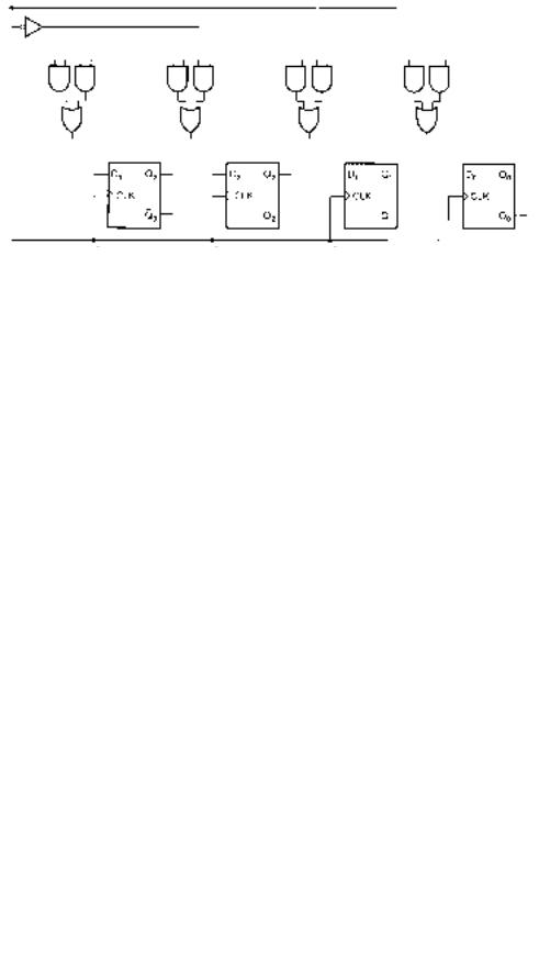
9.46Complete the logic circuit shown in Figure 9.91 to make a bidirectional shift register.
9.47Complete the logic circuit shown in Figure 9.92 to make a parallel-in-serial-out shift register.
9.8Programming Shift Registers in VHDL
9.48Write the VHDL code for an 8-bit serial shift register using a structural design procedure. Use JK flip-flops. (MAX PLUS II primitive: JKFF.) Create a MAX PLUS II simulation file to verify the operation of your design.
9.49 Repeat Problem 9.48 using a dataflow design procedure.
9.50Modify the VHDL code for the behaviorally designed shift register srg4behv.vhd so that the shift register moves the data left, not right. Hint: The statement
q (3 downto 0) <= serial_in & q(3 downto 1); is equivalent to the following two statements:
q(3) <= serial_in;
q(2 downto 0) <= q(3 downto 1);
Create a simulation file to verify the operation of this device.
FIGURE 9.92
Problem 9.47
Logic Circuit
9.51Modify the VHDL code for the left-shift register Problem 9.50 to make a shift register of generic width. Use this component in another VHDL file to make a 32-bit shift register that shifts left. Create a simulation file to verify the operation of this design.
9.52Write the code for a VHDL design entity that implements a 4-bit universal shift register with asynchronous clear. Create a simulation that verifies the design function.
9.53Use MAX PLUS II to create simulations for the generic-width and the 16-bit universal shift registers in Example 9.16 (p. 432). What is the difference in width between the default value of the generic shift register and the instantiated component in the 16-bit file? Given this difference, why can the generic-width shift register be correctly used as a component in the 16-bit design entity?
9.54Use an LPM shift register in a VHDL file to instantiate a 48-bit shift register with the following functions: serial input, parallel output, synchronous clear.
9.55Use an LPM shift register in a VHDL file to instantiate a 10-bit shift register with the following functions: serial input and output whose internal value can be synchro-

456 C H A P T E R 9 • Counters and Shift Registers
nously set to 960. Create a MAX PLUS II simulation to verify the operation of the design.
9.9Shift Register Counters
9.56Write the VHDL code for a ring counter of generic width and instantiate it as an 8-bit ring counter. List the sequence of states in a table, assuming the counter is initially cleared, and create a simulation to verify the circuit’s operation. Include a clear input (synchronous).
9.57Construct the count sequence table of a 5-bit Johnson counter, assuming the counter is initially cleared. What changes must be made to the decoder part of the circuit in Figure 9.84 (p. 446) if it is to decode the 5-bit Johnson counter?
“double twist” in the data path.
A N S W E R S T O S E C T I O N R E V I E W P R O B L E M S
Section 9.1
9.1 A mod-24 UP counter goes from 00000 to 10111 (0 to 23). This requires 5 outputs. The counter is a truncated sequence since its modulus is less than 25 32.
Section 9.2
9.2 1001, 0000
Section 9.3
9.3JK flip-flops: J3K3 X0, J2K2 1X, J1K1 X1, J0K0 X1 D flip-flops: D3 1, D2 1, D1 0, D0 0
Section 9.4
9.4 If (clock‘EVENT AND clock = ‘0’) THEN
count := count + 1;
END IF;
9.58A control sequence has ten steps, each activated by a logic HIGH. Use MAX PLUS II to design a counter and decoder in each of the following configurations to produce the required sequence: binary counter, ring counter, and Johnson counter. You may use a Graphic Design File or VHDL. Create a simulation for each counter and decoder.
9.59 Use the MAX PLUS II Graphic Editor to design a 4-bit ring counter that can be asynchronously initialized to Q3Q2Q1Q0 1000 by using only the clear inputs of its flip-flops. No presets allowed. Hint: use a circuit with a
Section 9.5
9.5 The completed timing diagram is shown in Figure 9.93.
Section 9.6
9.6 Asynchronous clear: PROCESS (clock, clear); Synchronous clear: PROCESS (clock)
Section 9.7
9.7 JK flip-flops can be used in the shift register of Figure 9.58. The Q output of any stage connects to the J input of the next stage and the Q output of any stage connects to the K input of the next. The serial_in input connects directly to the J input of the first flip-flop. Serial_in is applied to K of the first flip-flop through an inverter (NOT gate).
Section 9.8
9.8 A shift register output is defined as a port of mode BUFFER because this mode allows a signal to be fed back into the PLD matrix and reused as an input to another part of the circuit.
Section 9.9
Binary: 5 flip-flops, 24 5-inputs NANDs; Ring: 24 flip-flops, no
LOAD |
|
|
|
|
|
|
|
|
|
|
|
|
|
RESET |
|
|
|
|
|
|
|
|
|
|
|
|
|
CLOCK |
|
|
|
|
|
|
|
|
|
|
|
|
|
P |
0 |
|
|
|
|
|
8 |
|
|
|
|
5 |
|
QA 0 |
1 |
2 |
3 |
4 |
|
8 |
9 |
A |
0 |
1 |
2 |
5 |
6 |
QS 0 |
1 |
2 |
3 |
|
4 |
8 |
9 |
A |
0 |
1 |
2 |
|
5 6 |
FIGURE 9.93
Answer to Section Review Problem 9.5

C H A P T E R 10
State Machine Design
O U T L I N E C H A P T E R O B J E C T I V E S
10.1State Machines
10.2State Machines with No Control Inputs
10.3State Machines with Control Inputs
10.4Switch Debouncer for a Normally Open Pushbutton Switch
10.5Unused States in State Machines
10.6Traffic Light Controller
Upon successful completion of this chapter you will be able to:
•Describe the components of a state machine.
•Distinguish between Moore and Mealy implementations of state machines.
•Draw the state diagram of a state machine from a verbal description.
•Use the “classical” (state table) method of state machine design to determine the Boolean equations of the state machine.
•Translate the Boolean equations of a state machine into a Graphic Design File in Altera’s MAX PLUS II software.
•Write VHDL code to implement state machines.
•Create simulations in MAX PLUS II to verify the function of a state machine design.
•Determine whether the output of a state machine is vulnerable to asynchronous changes of input.
•Design state machine applications, such as a switch debouncer, a singlepulse generator, and a traffic light controller.
10.1 State Machines
K E Y T E R M S
State machine A synchronous sequential circuit, consisting of a sequential logic section and a combinational logic section, whose outputs and internal flip-flops progress through a predictable sequence of states in response to a clock and other input signals.
Moore machine A state machine whose output is determined only by the sequential logic of the machine.
Mealy machine A state machine whose output is determined by both the sequential logic and the combinational logic of the machine.
State variables The variables held in the flip-flops of a state machine that determine its present state. The number of state variables in a machine is equivalent to the number of flip-flops.
457

458 C H A P T E R 1 0 • State Machine Design
FIGURE 10.1
Moore-Type State Machine
The synchronous counters and shift registers we examined in Chapter 9 are examples of a larger class of circuits known as state machines. As described for synchronous counters in Section 9.2, a state machine consists of a memory section that holds the present state of the machine and a control section that determines the machine’s next state. These sections communicate via a series of command and status lines. Depending on the type of machine, the outputs will either be functions of the present state only or of the present and next states.
Figure 10.1 shows the block diagram of a Moore machine. The outputs of a Moore machine are determined solely by the present state of the machine’s memory section. The output may be directly connected to the Q outputs of the internal flip-flops, or the Q outputs might pass through a decoder circuit. The output of a Moore machine is synchronous to the system clock, since the output can only change when the machine’s internal state variables change.
The block diagram of a Mealy machine is shown in Figure 10.2. The outputs of the Mealy machine are derived from the combinational (control) section of the machine, as
FIGURE 10.2
Mealy-Type State Machine

10.2 • State Machines with No Control Inputs |
459 |
well as the sequential (memory) part of the machine. Therefore, the outputs can change asynchronously when the combinational circuit inputs change out of phase with the clock. (When we say that the outputs change asynchronously, we generally do not mean a change via a function such as asynchronous reset that directly affects the machine’s flip-flops.)
SECTION 10.1 REVIEW PROBLEM
10.1What is the main difference between a Moore-type state machine and a Mealy-type state machine?
10.2State Machines with No Control Inputs
K E Y T E R M S
Bubble A circle in a state diagram containing the state name and values of the
state variables.
A state machine can be designed using a classical technique, similar to that used to design a synchronous counter. We can also use a VHDL design method. We will design several state machines, using both classical and VHDL techniques.
As an example of these techniques, we will design a state machine whose output depends only on the clock input: a 3-bit counter with a Gray code count sequence. A 3-bit Gray code, shown in Table 10.1, changes only one bit between adjacent codes and is therefore not a binary-weighted sequence.
Table 10.1 3-bit Gray
Code Sequence
Q2Q1Q0
000
001
011
010
110
111
101
100
Gray code is often used in situations where it is important to minimize the effect of single-bit errors. For example, suppose the angle of a motor shaft is measured by a detected code on a Gray-coded shaft encoder, shown in Figure 10.3. The encoder indicates a 3-bit number for each of eight angular positions by having three concentric circular segments for each code. A dark band indicates a 1 and a transparent band indicates a 0, with the MSB as the outermost band. The dark or transparent bands are detected by three sensors that detect
FIGURE 10.3 |
100 |
000 |
Gray Code on a Shaft Encoder |
|
|
101 |
|
001 |
111 |
|
011 |
110 010