Dueck R.Digital design with CPLD applications and VHDL.2000
.pdf
9.7 • Shift Registers |
421 |
|
In |
|
|
0 |
1 |
2 |
3 |
|
|
|
|
Q |
Q |
Q |
Q |
|
|
|
Left Shift |
|
|
OUTPUT |
OUTPUT |
OUTPUT |
OUTPUT |
|
|
|
|
|
|
||||
|
INPUT |
|
PRN Q |
CLRN |
|
|
|
|
|
AND2 |
DFF |
|
|
|
|
||
|
|
|
|
|
|
|
||
|
OR2 |
D |
|
|
|
|
|
|
|
|
|
|
|
|
|
|
|
|
AND2 |
|
|
|
|
|
|
|
|
AND2 |
|
PRN Q |
CLRN |
|
|
|
|
|
OR2 |
DFF |
D |
|
|
|
|
|
|
|
|
|
|
|
|
|
|
|
AND2 |
|
|
|
|
|
|
|
|
AND2 |
DFF |
PRN Q |
CLRN |
|
|
|
|
|
|
|
|
|
|
|
||
|
OR2 |
D |
|
|
|
|
|
|
|
|
|
|
|
|
|
|
|
|
AND2 |
|
|
|
|
|
|
|
|
AND2 |
DFF |
PRN Q |
CLRN |
|
|
|
|
|
|
|
|
|
|
|
||
|
OR2 |
D |
|
|
|
|
|
|
|
|
|
|
|
|
|
|
|
|
AND2 |
|
|
|
|
|
|
|
|
NOT |
|
|
|
|
|
|
|
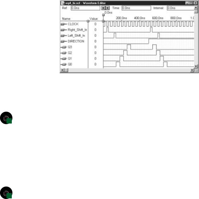
INPUT |
INPUT |
|
|
INPUT |
|
|
|
Register |
DIRECTION |
Right Shift In |
|
|
CLOCK |
|
|
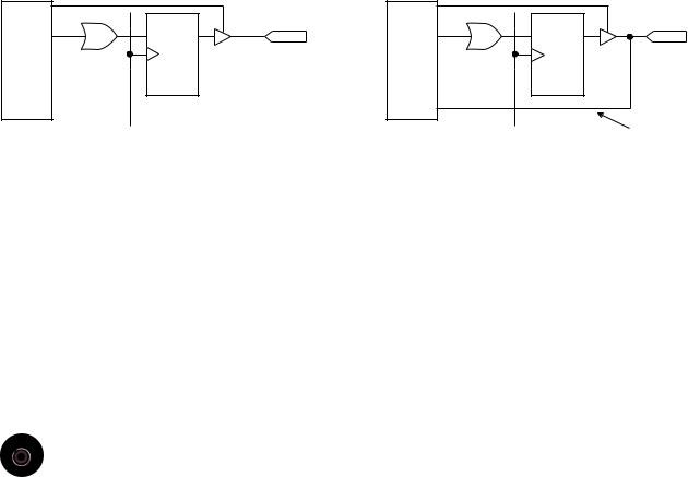
FIGURE 9.66 |
Bidirectional Shift |


424 C H A P T E R 9 • Counters and Shift Registers
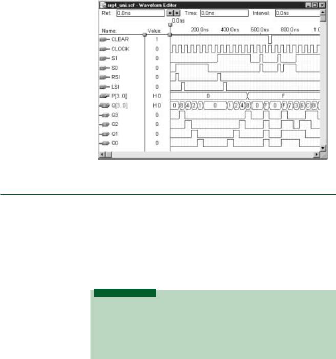
FIGURE 9.69
Simulation of a 4-bit Serial Shift Register with Parallel Load
Table 9.14 summarizes the various possible inputs to each flip-flop as a function of S1 and S0.
Table 9.14 Flip-Flop Inputs as a Function of S1S0 in a Universal Shift Register
S1 |
S0 |
Function |
D3 |
D2 |
D1 |
D0 |
0 |
0 |
Hold |
Q3 |
Q2 |
Q1 |
Q0 |
0 |
1 |
Shift Right |
RSI* |
Q3 |
Q2 |
Q1 |
1 |
0 |
Shift Left |
Q2 |
Q1 |
Q0 |
LSI** |
1 |
1 |
Load |
P3 |
P2 |
P1 |
P0 |
*RSI Right-shift input **LSI Left-shift input
EXAMPLE 9.14 |
Create a simulation file to verify the operation of the universal shift register of Figure 9.70. |
|
Solution Figure 9.71 shows a possible solution. The following functions are tested: |
|
hold, right shift (LSI ignored), hold, left shift (RSI ignored), load FH, asynchronous clear, |
|
load FH, shift right for two clocks, shift left for three clocks. |