
- •Introduction
- •ARM7TDMI Architecture
- •The THUMB Concept
- •THUMB’s Advantages
- •ARM7TDMI Block Diagram
- •ARM7TDMI Core Diagram
- •ARM7TDMI Functional Diagram
- •Key to signal types
- •Processor Operating States
- •Switching State
- •Entering THUMB state
- •Entering ARM state
- •Memory Formats
- •Big endian format
- •Little endian format
- •Instruction Length
- •Data Types
- •Operating Modes
- •Registers
- •The ARM state register set
- •The THUMB state register set
- •The relationship between ARM and THUMB state registers
- •Accessing Hi registers in THUMB state
- •The Program Status Registers
- •The condition code flags
- •The control bits
- •Exceptions
- •Action on entering an exception
- •Action on leaving an exception
- •Exception entry/exit summary
- •Notes
- •Abort
- •Software interrupt
- •Undefined instruction
- •Exception vectors
- •Exception priorities
- •Not all exceptions can occur at once:
- •Interrupt Latencies
- •Reset
- •Instruction Set Summary
- •Format summary
- •Instruction summary
- •The Condition Field
- •Branch and Exchange (BX)
- •Instruction cycle times
- •Assembler syntax
- •Using R15 as an operand
- •Examples
- •Branch and Branch with Link (B, BL)
- •The link bit
- •Instruction cycle times
- •Assembler syntax
- •Examples
- •Data Processing
- •CPSR flags
- •Shifts
- •Instruction specified shift amount
- •Register specified shift amount
- •Immediate operand rotates
- •Writing to R15
- •Using R15 as an operand
- •TEQ, TST, CMP and CMN opcodes
- •Instruction cycle times
- •Assembler syntax
- •where:
- •Examples
- •PSR Transfer (MRS, MSR)
- •Operand restrictions
- •Reserved bits
- •Example
- •Instruction cycle times
- •Assembler syntax
- •Examples
- •Multiply and Multiply-Accumulate (MUL, MLA)
- •If the operands are interpreted as signed
- •If the operands are interpreted as unsigned
- •Operand restrictions
- •CPSR flags
- •Instruction cycle times
- •Assembler syntax
- •Examples
- •Multiply Long and Multiply-Accumulate Long (MULL,MLAL)
- •Operand restrictions
- •CPSR flags
- •Instruction cycle times
- •For signed instructions SMULL, SMLAL:
- •For unsigned instructions UMULL, UMLAL:
- •Assembler syntax
- •where:
- •Examples
- •Single Data Transfer (LDR, STR)
- •Offsets and auto-indexing
- •Shifted register offset
- •Bytes and words
- •Little endian configuration
- •Big endian configuration
- •Restriction on the use of base register
- •Example:
- •Data aborts
- •Instruction cycle times
- •Assembler syntax
- •Examples
- •Halfword and Signed Data Transfer(LDRH/STRH/LDRSB/LDRSH)
- •Offsets and auto-indexing
- •Halfword load and stores
- •Signed byte and halfword loads
- •Endianness and byte/halfword selection
- •Little endian configuration
- •Big endian configuration
- •Data aborts
- •Instruction cycle times
- •Assembler syntax
- •Examples
- •Block Data Transfer (LDM, STM)
- •The register list
- •Addressing modes
- •Address alignment
- •LDM with R15 in transfer list and S bit set (Mode changes)
- •STM with R15 in transfer list and S bit set (User bank transfer)
- •R15 not in list and S bit set (User bank transfer)
- •Use of R15 as the base
- •Inclusion of the base in the register list
- •Data aborts
- •Aborts during STM instructions
- •Aborts during LDM instructions
- •Instruction cycle times
- •Assembler syntax
- •Addressing mode names
- •Examples
- •Single Data Swap (SWP)
- •Bytes and words
- •Data aborts
- •Instruction cycle times
- •Assembler syntax
- •Examples
- •Software Interrupt (SWI)
- •Return from the supervisor
- •Comment field
- •Instruction cycle times
- •Assembler syntax
- •Examples
- •Supervisor code
- •Coprocessor Data Operations (CDP)
- •The coprocessor fields
- •Instruction cycle times
- •Assembler syntax
- •Examples
- •Coprocessor Data Transfers (LDC, STC)
- •The coprocessor fields
- •Addressing modes
- •Address alignment
- •Data aborts
- •Instruction cycle times
- •Assembler syntax
- •Examples
- •Coprocessor Register Transfers (MRC, MCR)
- •The coprocessor fields
- •Transfers to R15
- •Transfers from R15
- •Instruction cycle times
- •Assembler syntax
- •Examples
- •Undefined Instruction
- •Instruction cycle times
- •Assembler syntax
- •Instruction Set Examples
- •Using the conditional instructions
- •Using conditionals for logical OR
- •Absolute value
- •Multiplication by 4, 5 or 6 (run time)
- •Combining discrete and range tests
- •Division and remainder
- •Overflow detection in the ARM7TDMI
- •Pseudo-random binary sequence generator
- •Multiplication by constant using the barrel shifter
- •Multiplication by 2^n (1,2,4,8,16,32..)
- •Multiplication by 2^n+1 (3,5,9,17..)
- •Multiplication by 2^n-1 (3,7,15..)
- •Multiplication by 6
- •Multiply by 10 and add in extra number
- •General recursive method for Rb := Ra*C, C a constant:
- •Loading a word from an unknown alignment
- •Format Summary
- •Opcode Summary
- •Format 1: move shifted register
- •Operation
- •Instruction cycle times
- •Examples
- •Format 2: add/subtract
- •Operation
- •Instruction cycle times
- •Examples
- •Format 3: move/compare/add/subtract immediate
- •Operations
- •Instruction cycle times
- •Examples
- •Format 4: ALU operations
- •Operation
- •Instruction cycle times
- •Examples
- •Format 5: Hi register operations/branch exchange
- •Operation
- •Instruction cycle times
- •The BX instruction
- •Examples
- •Using R15 as an operand
- •Format 6: PC-relative load
- •Operation
- •Instruction cycle times
- •Examples
- •Format 7: load/store with register offset
- •Operation
- •Instruction cycle times
- •Examples
- •Format 8: load/store sign-extended byte/halfword
- •Operation
- •Instruction cycle times
- •Examples
- •Format 9: load/store with immediate offset
- •Operation
- •Instruction cycle times
- •Examples
- •Format 10: load/store halfword
- •Operation
- •Instruction cycle times
- •Examples
- •Format 11: SP-relative load/store
- •Operation
- •Instruction cycle times
- •Examples
- •Format 12: load address
- •Operation
- •Instruction cycle times
- •Examples
- •Format 13: add offset to Stack Pointer
- •Operation
- •Instruction cycle times
- •Examples
- •Format 14: push/pop registers
- •Operation
- •Instruction cycle times
- •Examples
- •Format 15: multiple load/store
- •Operation
- •Instruction cycle times
- •Examples
- •Format 16: conditional branch
- •Operation
- •Instruction cycle times
- •Examples
- •Format 17: software interrupt
- •Operation
- •Instruction cycle times
- •Examples
- •Format 18: unconditional branch
- •Operation
- •Examples
- •Format 19: long branch with link
- •Operation
- •Instruction cycle times
- •Examples
- •Instruction Set Examples
- •Multiplication by a constant using shifts and adds
- •General purpose signed divide
- •Thumb code
- •ARM code
- •Division by a constant
- •Explanation of divide-by-constant ARM code
- •ARM code
- •THUMB code
- •Overview
- •Cycle Types
- •Address Timing
- •Data Transfer Size
- •Instruction Fetch
- •Memory Management
- •Locked Operations
- •Stretching Access Times
- •The ARM Data Bus
- •The External Data Bus
- •The unidirectional data bus
- •The bidirectional data bus
- •Example system: The ARM7TDMI Testchip
- •Overview
- •Interface Signals
- •Coprocessor present/absent
- •Busy-waiting
- •Pipeline following
- •Data transfer cycles
- •Register Transfer Cycle
- •Privileged Instructions
- •Idempotency
- •Undefined Instructions
- •Debug Interface
- •Overview
- •Debug Systems
- •Debug Interface Signals
- •Entry into debug state
- •Entry into debug state on breakpoint
- •Entry into debug state on watchpoint
- •Entry into debug state on debug-request
- •Action of ARM7TDMI in debug state
- •Scan Chains and JTAG Interface
- •Scan limitations
- •Scan chain 0
- •Scan chain 1
- •Scan Chain 2
- •The JTAG state machine
- •Reset
- •Pullup Resistors
- •Instruction Register
- •Public Instructions
- •EXTEST (0000)
- •SCAN_N (0010)
- •INTEST (1100)
- •IDCODE (1110)
- •BYPASS (1111)
- •CLAMP (0101)
- •HIGHZ (0111)
- •CLAMPZ (1001)
- •SAMPLE/PRELOAD (0011)
- •RESTART (0100)
- •Test Data Registers
- •Bypass register
- •ARM7TDMI device identification (ID) code register
- •Operating mode:
- •Instruction register
- •Scan chain select register
- •Scan chains 0,1 and 2
- •Scan chain 0 and 1
- •Scan chain 0
- •Scan chain 1
- •Scan chain 3
- •ARM7TDMI Core Clocks
- •Clock switch during debug
- •Clock switch during test
- •Determining the Core and System State
- •Determining the core’s state
- •Determining system state
- •Exit from debug state
- •The PC’s Behaviour During Debug
- •Breakpoint
- •Watchpoints
- •Watchpoint with another exception
- •Debug request
- •System speed access
- •Summary of return address calculations
- •Priorities / Exceptions
- •Breakpoint with prefetch abort
- •Interrupts
- •Data aborts
- •Scan Interface Timing
- •Debug Timing
- •Overview
- •The Watchpoint Registers
- •Programming and reading watchpoint registers
- •Using the mask registers
- •The control registers
- •Programming Breakpoints
- •Hardware breakpoints:
- •Software breakpoints:
- •Hardware breakpoints
- •Software breakpoints
- •Setting the breakpoint
- •Clearing the breakpoint
- •Programming Watchpoints
- •The Debug Control Register
- •Debug Status Register
- •Coupling Breakpoints and Watchpoints
- •Example
- •CHAINOUT signal
- •RANGEOUT signal
- •Example
- •Disabling ICEBreaker
- •ICEBreaker Timing
- •Programming Restriction
- •Debug Communications Channel
- •Debug comms channel registers
- •Communications via the comms channel
- •Introduction
- •Branch and Branch with Link
- •THUMB Branch with Link
- •Branch and Exchange (BX)
- •Data Operations
- •Multiply and Multiply Accumulate
- •Load Register
- •Store Register
- •Load Multiple Registers
- •Store Multiple Registers
- •Data Swap
- •Software Interrupt and Exception Entry
- •Coprocessor Data Operation
- •Coprocessor Data Transfer (from memory to coprocessor)
- •Coprocessor Data Transfer (from coprocessor to memory)
- •Coprocessor Register Transfer (Load from coprocessor)
- •Coprocessor Register Transfer (Store to coprocessor)
- •Undefined Instructions and Coprocessor Absent
- •Unexecuted Instructions
- •Instruction Speed Summary
- •Timing Diagrams

Determining the Core and System State
When ARM7TDMI is in debug state, the core and system’s state may be examined. This is done by forcing load and store multiples into the instruction pipeline.
Before the core and system state can be examined, the debugger must first determine whether the processor was in THUMB or ARM state when it entered debug. This is achieved by examining bit 4 of ICEbreaker’s Debug Status Register. If this is HIGH, the core was in THUMB state when it entered debug.
Determining the core’s state
If the processor has entered debug state from THUMB state, the simplest course of action is for the debugger to force the core back into ARM state. Once this is done, the debugger can always execute the same sequence of instructions to determine the processor’s state.
To force the processor into ARM state, the following sequence of THUMB instructions should be executed on the core:
STR |
R0, [R0] ; Save R0 before use |
|
MOV |
R0, PC |
; Copy PC into R0 |
STR |
R0, [R0] ; Now save the PC in R0 |
|
BX |
PC |
; Jump into ARM state |
MOV |
R8, R8 |
; NOP |
MOV |
R8, R8 |
; NOP |
Note: Since all THUMB instructions are only 16 bits long, the simplest course of action when shifting them into Scan Chain 1 is to repeat the instruction twice. For example, the encoding for BX R0 is 0x4700. Thus if 0x47004700 is shifted into scan chain 1, the debugger does not have to keep track of which half of the bus the processor expects to read the data from.
From this point on, the processor’s state can be determined by the sequences of ARM instructions described below.
Once the processor is in ARM state, typically the first instruction executed would be:
STM R0, {R0-R15}
This causes the contents of the registers to be made visible on the data bus. These values can then be sampled and shifted out.
Note: The above use of R0 as the base register for the STM is for illustration only, any register could be used.
After determining the values in the current bank of registers, it may be desirable to access the banked registers. This can only be done by changing mode. Normally, a mode change may only occur if the core is already in a privileged mode. However, while in debug state, a mode change from any mode into any other mode may occur. Note that the debugger must restore the original mode before exiting debug state.
For example, assume that the debugger had been asked to return the state of the USER mode and FIQ mode registers, and debug state was entered in supervisor mode.
The instruction sequence could be:
STM R0, {R0-R15}; Save |
current registers |
|
MRS R0, CPSR |
|
|
STR R0, R0 |
; Save CPSR to determine current mode |
|
BIC R0, 0x1F |
; Clear |
mode bits |
ORR R0, 0x10 |
; Select user mode |
|
MSR CPSR, R0 |
; Enter |
USER mode |
STM R0, {R13,R14}; Save |
register not previously visible |
||||
ORR R0, |
0x01 |
; |
Select |
FIQ mode |
|
MSR |
CPSR, R0 |
; |
Enter |
FIQ mode |
|
STM |
R0, |
{R8-R14}; Save |
banked FIQ registers |
152 |
Debug |
|
|
||
|

All these instructions are said to execute at debug speed. Debug speed is much slower than system speed since between each core clock, 33 scan clocks occur in order to shift in an instruction, or shift out data. Executing instructions more slowly than usual is fine for accessing the core’s state since ARM7TDMI is fully static. However, this same method cannot be used for determining the state of the rest of the system.
While in debug state, only the following instructions may legally be scanned into the instruction pipeline for execution:
•all data processing operations, except TEQP
•all load, store, load multiple and store multiple instructions
•MSR and MRS
Determining system state
In order to meet the dynamic timing requirements of the memory system, any attempt to access system state must occur synchronously to it. Thus, ARM7TDMI must be forced to synchronise back to system speed. This is controlled by the 33rd bit of scan chain 1.
Any instruction may be placed in scan chain 1 with bit 33 (the BREAKPT bit) LOW. This instruction will then be executed at debug speed. To execute an instruction at system speed, the instruction prior to it must be scanned into scan chain 1 with bit 33 set HIGH.
After the system speed instruction has been scanned into the data bus and clocked into the pipeline, the BYPASS instruction must be loaded into the TAP controller. This will cause ARM7TDMI to automatically synchronise back to MCLK (the system clock), execute the instruction at system speed, and then re-enter debug state and switch itself back to the internally generated DCLK. When the instruction has completed, DBGACK will be HIGH and the core will have switched back to DCLK. At this point, INTEST can be selected in the TAP controller, and debugging can resume.
In order to determine that a system speed instruction has completed, the debugger must look at both DBGACK and nMREQ. In order to access memory, ARM7TDMI drives nMREQ LOW after it has synchronised back to system speed. This transition is used by the memory controller to arbitrate whether ARM7TDMI can have the bus in the next cycle. If the bus is not available, ARM7TDMI may have its clock stalled indefinitely. Therefore, the only way to tell that the memory access has completed, is to examine the state of both nMREQ and DBGACK. When both are HIGH, the access has completed. Usually, the debugger would be using ICEBreaker to control debugging, and by reading ICEBreaker's status register, the state of nMREQ and DBGACK can be determined. Refer to ICEBreaker Module on page 163 for more details.
Debug
By the use of system speed load multiples and debug speed store multiples, the state of the system’s memory can be fed back to the debug host.
There are restrictions on which instructions may have the 33rd bit set. The only valid instructions on which to set this bit are loads, stores, load multiple and store multiple. See also <Reference><body> Exit from debug state<body>. When ARM7TDMI returns to debug state after a system speed access, bit 33 of scan chain 1 is set HIGH. This gives the debugger information about why the core entered debug state the first time this scan chain is read.
Exit from debug state
Leaving debug state involves restoring ARM7TDMI’s internal state, causing a branch to the next instruction to be executed, and synchronising back to MCLK. After restoring internal state, a branch instruction must be loaded into the pipeline. See The PC’s Behaviour During Debug on page 155 for details on calculating the branch.
Bit 33 of scan chain 1 is used to force ARM7TDMI to resynchronise back to MCLK. The penultimate instruction of the debug sequence is scanned in with bit 33 set HIGH. The final instruction of the debug sequence is the branch, and this is scanned in with bit 33 LOW. The core is then clocked to load the branch into the pipeline. Now, the RESTART instruction is selected in the TAP controller. When the state machine enters the RUN-TEST/IDLE state, the scan chain will revert back to system mode and clock resynchronisation to MCLK will occur within ARM7TDMI. ARM7TDMI will then resume normal operation, fetching instructions from memory. This delay, until the state machine is in the RUNTEST/IDLE state, allows conditions to be set up in other devices in a multiprocessor system without taking immediate effect. Then, when the RUN-TEST/IDLE state is entered, all the processors resume operation simultaneously.
The function of DBGACK is to tell the rest of the system when ARM7TDMI is in debug state. This can be used to inhibit peripherals such as watchdog timers which have real time characteristics. Also, DBGACK can be used to mask out memory accesses which are caused by the debugging process. For example, when ARM7TDMI enters debug state after a breakpoint, the instruction pipeline contains the breakpointed instruction plus two other instructions which have been prefetched. On entry to debug state, the pipeline is flushed. Therefore, on exit from debug state, the pipeline must be refilled to its previous state. Thus, because of the debugging process, more memory accesses occur than would normally be expected. Any system peripheral which may be sensitive to the number of memory accesses can be inhibited through the use of
DBGACK.
153

For example, imagine a fictitious peripheral that simply counts the number of memory cycles. This device should return the same answer after a program has been run both
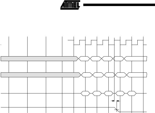
Figure 81. Debug Exit Sequence
ECLK |
|
|
|
|
|
|
|
|
|
|
|
|
|
|
|
|
|
|
|
nMREQ |
|
|
|
Internal Cycles |
|
|
|
||
SEQ |
|
|
|
|
|
|
|||
|
|
|
|
|
|
|
|
||
A[31:0] |
|
|
|
|
|
|
|
|
|
D[31:0] |
|
|
|
|
|
|
|
|
DBGACK
It can be seen from Figure 76 that the final memory access occurs in the cycle after DBGACK goes HIGH, and this is the point at which the cycle counter should be disabled. Figure 81 shows that the first memory access that the cycle counter has not seen before occurs in the cycle after DBGACK goes LOW, and so this is the point at which the counter should be re-enabled.
Note that when a system speed access from debug state occurs, ARM7TDMI temporarily drops out of debug state, and so DBGACK can go LOW. If there are peripherals which are sensitive to the number of memory accesses, they must be led to believe that ARM7TDMI is still in debug state. By programming the ICEBreaker control register, the value on DBGACK can be forced to be HIGH. See ICEBreaker Module on page 163 for more details.
with and without debugging. Figure 81 shows the behaviour of ARM7TDMI on exit from the debug state.
N S S
Ab Ab+4 Ab+8
154 |
Debug |
|
|
||
|