

Memory
The External Data Bus
ARM7TDMI has a bidirectional data bus, D[31:0]. However, since some ASIC design methodologies prohibit the use of bidirectional buses, unidirectional data in, DIN[31:0],
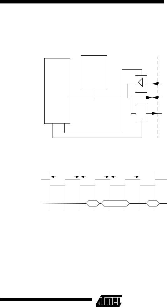
Figure 67. ARM7TDMI External Bus Arrangement
and data out, DOUT[31:0], busses are also provided. The logical arrangement of these buses is shown inFigure 67.
|
ICEbreaker |
ARM7TDMI |
DIN[31:0] |
|
|
|
D[31:0] |
|
DOUT[31:0] |
|
G |
When the bidirectional data bus is being used, the unidirectional busses must be disabled by driving BUSEN LOW.
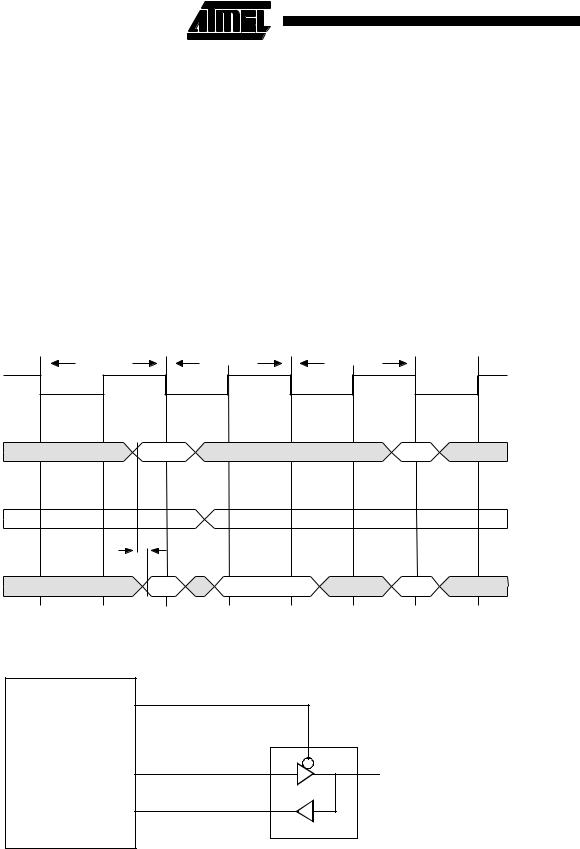
Figure 68. Bidirectional Bus Timing
The timing of the bus for three cycles, load-store-load, is shown in Figure 68.
Read Cycle |
Store Cycle |
Read Cycle |
MCLK |
|
|
APE |
|
|
129
The unidirectional data bus
When the unidirectional data busses are being used, (i.e. when BUSEN is HIGH), the bidirectional bus, D[31:0], must be left unconnected.
When BUSEN is HIGH, all instructions and input data are presented on the input data bus, DIN[31:0]. The timing of this data is similar to that of the bidirectional bus when in input mode. Data must be set up and held to the falling edge of MCLK. For the exact timing requirements refer to Timing Diagrams on page 189.
In this configuration, all output data is presented on DOUT[31:0]. The value on this bus only changes when the processor performs a store cycle. Again, the timing of the data is similar to that of the bidirectional data bus. The
Figure 69. Unidirectional Bus Timing
value on DOUT[31:0] changes off the falling edge of
MCLK.
The bus timing of a read-write-read cycle combination is shown in Figure 69.
When BUSEN is LOW, the buffer between DIN[31:0] and D[31:0] is disabled. Any data presented on DIN[31:0] is ignored. Also, when B U S E N is low, the value on DOUT[31:0] is forced to 0x00000000.
Typically, the unidirectional busses would be used internally in ASIC embedded applications. Externally, most systems still require a bidirectional data bus to interface to external memory. Figure 70 shows how the unidirectional busses may be joined up at the pads of an ASIC to connect to an external bidirectional bus.
Read Cycle |
Store Cycle |
Read Cycle |
MCLK
DIN[31:0] |
D1 |
D2 |
DOUT[31:0] |
Dout |
D[31:0] |
D1 |
Dout |
D2 |
Figure 70. External Connection of Unidirectional Busses
|
nENOUT |
ARM7TDMI |
PAD |
|
|
|
DOUT[31:0] |
|
XDATA[31:0] |
|
DIN[31:0] |
130 |
Memory |
|
|
||
|
Memory
The bidirectional data bus
ARM7TDMI has a bidirectional data bus, D[31:0]. Most of the time, the ARM reads from memory and so this bus is configured to input. During write cycles however, the ARM7TDMI must output data. During phase 2 of the previous cycle, the signal nRW is driven HIGH to indicate a write cycle. During the actual cycle, nENOUT is driven LOW to
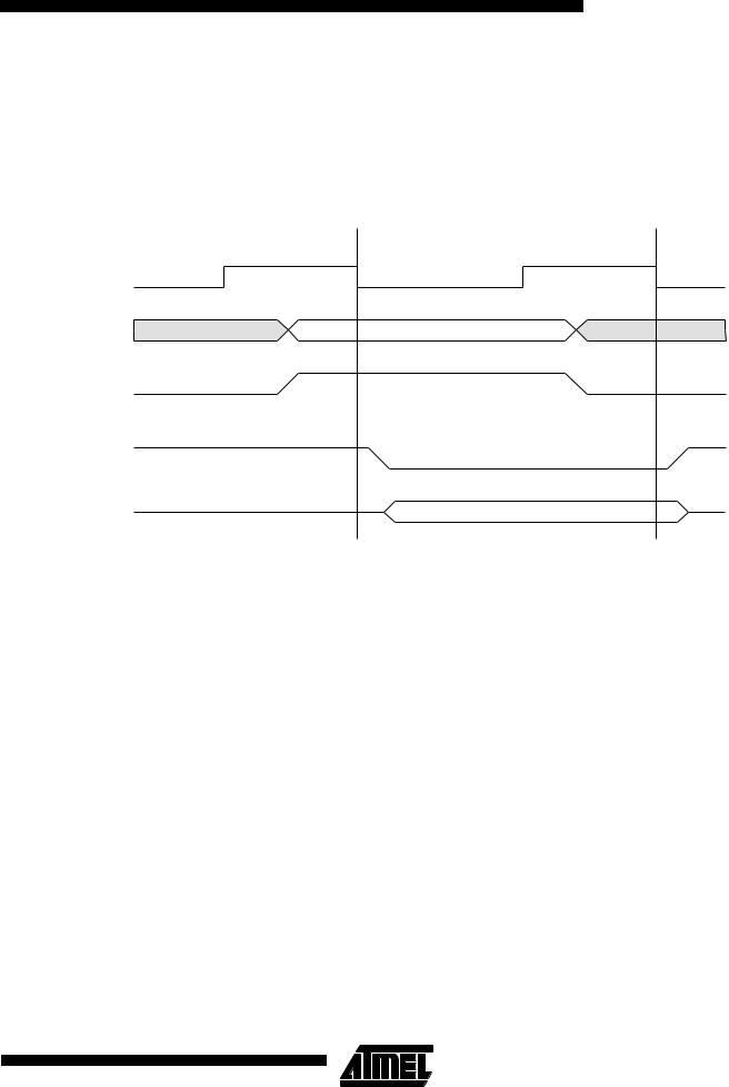
Figure 71. Data Write Bus Cycle
MCLK
A[31:0]
nRW
nENOUT
D[31:0]
indicate that the ARM7TDMI is driving D[31:0] as an output. Figure 71 shows this bus timing (DBE has been tied HIGH in this example). Figure 73 on page 133 shows the circuit which exists in ARM7TDMI for controlling exactly when the external bus is driven out.
Memory Cycle
The ARM7TDMI macrocell has an additional bus control signal, nENIN, which allows the external system to manually tristate the bus. In the simplest systems, nENIN can be tied LOW and nENOUT can be ignored. However, in many applications when the external data bus is a shared resource, greater control may be required. In this situation, nENIN can be used to delay when the external bus is driven. Note that for backwards compatibility, DBE is also included. At the macrocell level, DBE and nENIN have almost identical functionality and in most applications one can be tied off.
The Section Example system: The ARM7TDMI Testchip on page 133 describes how ARM7TDMI may be interfaced to an external data bus, using ARM7TDMI Testchip as an example.
ARM7TDMI has another output control signal called TBE. This signal is normally only used during test and must be tied HIGH when not in use. When driven LOW, TBE forces all three-stateable outputs to high impedance. It is as if both DBE and ABE have been driven LOW, causing the data bus, the address bus, and all other signals normally controlled by ABE to become high impedance. Note, however, that there is no scan cell on TBE. Thus, TBE is completely independent of scan data and may be used to put the outputs into a high impedance state while scan testing takes place.
Table 33 below, shows the tri-state control of ARM7TDMI’s outputs.
Signals without in the ABE, DBE or TBE column cannot be driven to the high impedance state:
Table 33. Output Enable Control Summary
ARM7TDMI output |
ABE |
DBE |
TBE |
A[31:0] |
|
|
|
|
|
|
|
D[31:0] |
|
|
|
|
|
|
|
nRW |
|
|
|
|
|
|
|
LOCK |
|
|
|
|
|
|
|
MAS[1:0] |
|
|
|
|
|
|
|
nOPC |
|
|
|
|
|
|
|
nTRANS |
|
|
|
|
|
|
|
DBGACK |
|
|
|
|
|
|
|
131
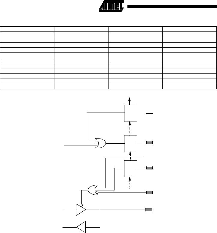
Table 33. Output Enable Control Summary
ARM7TDMI output |
ABE |
DBE |
TBE |
ECLK
nCPI
nENOUT
nEXEC
nM[4:0]
TBIT
nMREQ
SDOUTMS
SDOUTDATA
SEQ
DOUT[31:0]
Figure 72. ARM7TDMI Data Bus Control Circuit
Scan 
 DBE
DBE
Cell
Core Control |
Scan |
nENOUT |
|
Cell |
|
|
|
|
|
Scan |
nENIN |
|
Cell |
|
|
|
|
|
|
TBE |
|
|
D[31:0] |
132 |
Memory |
|
|
||
|