
- •Introduction
- •ARM7TDMI Architecture
- •The THUMB Concept
- •THUMB’s Advantages
- •ARM7TDMI Block Diagram
- •ARM7TDMI Core Diagram
- •ARM7TDMI Functional Diagram
- •Key to signal types
- •Processor Operating States
- •Switching State
- •Entering THUMB state
- •Entering ARM state
- •Memory Formats
- •Big endian format
- •Little endian format
- •Instruction Length
- •Data Types
- •Operating Modes
- •Registers
- •The ARM state register set
- •The THUMB state register set
- •The relationship between ARM and THUMB state registers
- •Accessing Hi registers in THUMB state
- •The Program Status Registers
- •The condition code flags
- •The control bits
- •Exceptions
- •Action on entering an exception
- •Action on leaving an exception
- •Exception entry/exit summary
- •Notes
- •Abort
- •Software interrupt
- •Undefined instruction
- •Exception vectors
- •Exception priorities
- •Not all exceptions can occur at once:
- •Interrupt Latencies
- •Reset
- •Instruction Set Summary
- •Format summary
- •Instruction summary
- •The Condition Field
- •Branch and Exchange (BX)
- •Instruction cycle times
- •Assembler syntax
- •Using R15 as an operand
- •Examples
- •Branch and Branch with Link (B, BL)
- •The link bit
- •Instruction cycle times
- •Assembler syntax
- •Examples
- •Data Processing
- •CPSR flags
- •Shifts
- •Instruction specified shift amount
- •Register specified shift amount
- •Immediate operand rotates
- •Writing to R15
- •Using R15 as an operand
- •TEQ, TST, CMP and CMN opcodes
- •Instruction cycle times
- •Assembler syntax
- •where:
- •Examples
- •PSR Transfer (MRS, MSR)
- •Operand restrictions
- •Reserved bits
- •Example
- •Instruction cycle times
- •Assembler syntax
- •Examples
- •Multiply and Multiply-Accumulate (MUL, MLA)
- •If the operands are interpreted as signed
- •If the operands are interpreted as unsigned
- •Operand restrictions
- •CPSR flags
- •Instruction cycle times
- •Assembler syntax
- •Examples
- •Multiply Long and Multiply-Accumulate Long (MULL,MLAL)
- •Operand restrictions
- •CPSR flags
- •Instruction cycle times
- •For signed instructions SMULL, SMLAL:
- •For unsigned instructions UMULL, UMLAL:
- •Assembler syntax
- •where:
- •Examples
- •Single Data Transfer (LDR, STR)
- •Offsets and auto-indexing
- •Shifted register offset
- •Bytes and words
- •Little endian configuration
- •Big endian configuration
- •Restriction on the use of base register
- •Example:
- •Data aborts
- •Instruction cycle times
- •Assembler syntax
- •Examples
- •Halfword and Signed Data Transfer(LDRH/STRH/LDRSB/LDRSH)
- •Offsets and auto-indexing
- •Halfword load and stores
- •Signed byte and halfword loads
- •Endianness and byte/halfword selection
- •Little endian configuration
- •Big endian configuration
- •Data aborts
- •Instruction cycle times
- •Assembler syntax
- •Examples
- •Block Data Transfer (LDM, STM)
- •The register list
- •Addressing modes
- •Address alignment
- •LDM with R15 in transfer list and S bit set (Mode changes)
- •STM with R15 in transfer list and S bit set (User bank transfer)
- •R15 not in list and S bit set (User bank transfer)
- •Use of R15 as the base
- •Inclusion of the base in the register list
- •Data aborts
- •Aborts during STM instructions
- •Aborts during LDM instructions
- •Instruction cycle times
- •Assembler syntax
- •Addressing mode names
- •Examples
- •Single Data Swap (SWP)
- •Bytes and words
- •Data aborts
- •Instruction cycle times
- •Assembler syntax
- •Examples
- •Software Interrupt (SWI)
- •Return from the supervisor
- •Comment field
- •Instruction cycle times
- •Assembler syntax
- •Examples
- •Supervisor code
- •Coprocessor Data Operations (CDP)
- •The coprocessor fields
- •Instruction cycle times
- •Assembler syntax
- •Examples
- •Coprocessor Data Transfers (LDC, STC)
- •The coprocessor fields
- •Addressing modes
- •Address alignment
- •Data aborts
- •Instruction cycle times
- •Assembler syntax
- •Examples
- •Coprocessor Register Transfers (MRC, MCR)
- •The coprocessor fields
- •Transfers to R15
- •Transfers from R15
- •Instruction cycle times
- •Assembler syntax
- •Examples
- •Undefined Instruction
- •Instruction cycle times
- •Assembler syntax
- •Instruction Set Examples
- •Using the conditional instructions
- •Using conditionals for logical OR
- •Absolute value
- •Multiplication by 4, 5 or 6 (run time)
- •Combining discrete and range tests
- •Division and remainder
- •Overflow detection in the ARM7TDMI
- •Pseudo-random binary sequence generator
- •Multiplication by constant using the barrel shifter
- •Multiplication by 2^n (1,2,4,8,16,32..)
- •Multiplication by 2^n+1 (3,5,9,17..)
- •Multiplication by 2^n-1 (3,7,15..)
- •Multiplication by 6
- •Multiply by 10 and add in extra number
- •General recursive method for Rb := Ra*C, C a constant:
- •Loading a word from an unknown alignment
- •Format Summary
- •Opcode Summary
- •Format 1: move shifted register
- •Operation
- •Instruction cycle times
- •Examples
- •Format 2: add/subtract
- •Operation
- •Instruction cycle times
- •Examples
- •Format 3: move/compare/add/subtract immediate
- •Operations
- •Instruction cycle times
- •Examples
- •Format 4: ALU operations
- •Operation
- •Instruction cycle times
- •Examples
- •Format 5: Hi register operations/branch exchange
- •Operation
- •Instruction cycle times
- •The BX instruction
- •Examples
- •Using R15 as an operand
- •Format 6: PC-relative load
- •Operation
- •Instruction cycle times
- •Examples
- •Format 7: load/store with register offset
- •Operation
- •Instruction cycle times
- •Examples
- •Format 8: load/store sign-extended byte/halfword
- •Operation
- •Instruction cycle times
- •Examples
- •Format 9: load/store with immediate offset
- •Operation
- •Instruction cycle times
- •Examples
- •Format 10: load/store halfword
- •Operation
- •Instruction cycle times
- •Examples
- •Format 11: SP-relative load/store
- •Operation
- •Instruction cycle times
- •Examples
- •Format 12: load address
- •Operation
- •Instruction cycle times
- •Examples
- •Format 13: add offset to Stack Pointer
- •Operation
- •Instruction cycle times
- •Examples
- •Format 14: push/pop registers
- •Operation
- •Instruction cycle times
- •Examples
- •Format 15: multiple load/store
- •Operation
- •Instruction cycle times
- •Examples
- •Format 16: conditional branch
- •Operation
- •Instruction cycle times
- •Examples
- •Format 17: software interrupt
- •Operation
- •Instruction cycle times
- •Examples
- •Format 18: unconditional branch
- •Operation
- •Examples
- •Format 19: long branch with link
- •Operation
- •Instruction cycle times
- •Examples
- •Instruction Set Examples
- •Multiplication by a constant using shifts and adds
- •General purpose signed divide
- •Thumb code
- •ARM code
- •Division by a constant
- •Explanation of divide-by-constant ARM code
- •ARM code
- •THUMB code
- •Overview
- •Cycle Types
- •Address Timing
- •Data Transfer Size
- •Instruction Fetch
- •Memory Management
- •Locked Operations
- •Stretching Access Times
- •The ARM Data Bus
- •The External Data Bus
- •The unidirectional data bus
- •The bidirectional data bus
- •Example system: The ARM7TDMI Testchip
- •Overview
- •Interface Signals
- •Coprocessor present/absent
- •Busy-waiting
- •Pipeline following
- •Data transfer cycles
- •Register Transfer Cycle
- •Privileged Instructions
- •Idempotency
- •Undefined Instructions
- •Debug Interface
- •Overview
- •Debug Systems
- •Debug Interface Signals
- •Entry into debug state
- •Entry into debug state on breakpoint
- •Entry into debug state on watchpoint
- •Entry into debug state on debug-request
- •Action of ARM7TDMI in debug state
- •Scan Chains and JTAG Interface
- •Scan limitations
- •Scan chain 0
- •Scan chain 1
- •Scan Chain 2
- •The JTAG state machine
- •Reset
- •Pullup Resistors
- •Instruction Register
- •Public Instructions
- •EXTEST (0000)
- •SCAN_N (0010)
- •INTEST (1100)
- •IDCODE (1110)
- •BYPASS (1111)
- •CLAMP (0101)
- •HIGHZ (0111)
- •CLAMPZ (1001)
- •SAMPLE/PRELOAD (0011)
- •RESTART (0100)
- •Test Data Registers
- •Bypass register
- •ARM7TDMI device identification (ID) code register
- •Operating mode:
- •Instruction register
- •Scan chain select register
- •Scan chains 0,1 and 2
- •Scan chain 0 and 1
- •Scan chain 0
- •Scan chain 1
- •Scan chain 3
- •ARM7TDMI Core Clocks
- •Clock switch during debug
- •Clock switch during test
- •Determining the Core and System State
- •Determining the core’s state
- •Determining system state
- •Exit from debug state
- •The PC’s Behaviour During Debug
- •Breakpoint
- •Watchpoints
- •Watchpoint with another exception
- •Debug request
- •System speed access
- •Summary of return address calculations
- •Priorities / Exceptions
- •Breakpoint with prefetch abort
- •Interrupts
- •Data aborts
- •Scan Interface Timing
- •Debug Timing
- •Overview
- •The Watchpoint Registers
- •Programming and reading watchpoint registers
- •Using the mask registers
- •The control registers
- •Programming Breakpoints
- •Hardware breakpoints:
- •Software breakpoints:
- •Hardware breakpoints
- •Software breakpoints
- •Setting the breakpoint
- •Clearing the breakpoint
- •Programming Watchpoints
- •The Debug Control Register
- •Debug Status Register
- •Coupling Breakpoints and Watchpoints
- •Example
- •CHAINOUT signal
- •RANGEOUT signal
- •Example
- •Disabling ICEBreaker
- •ICEBreaker Timing
- •Programming Restriction
- •Debug Communications Channel
- •Debug comms channel registers
- •Communications via the comms channel
- •Introduction
- •Branch and Branch with Link
- •THUMB Branch with Link
- •Branch and Exchange (BX)
- •Data Operations
- •Multiply and Multiply Accumulate
- •Load Register
- •Store Register
- •Load Multiple Registers
- •Store Multiple Registers
- •Data Swap
- •Software Interrupt and Exception Entry
- •Coprocessor Data Operation
- •Coprocessor Data Transfer (from memory to coprocessor)
- •Coprocessor Data Transfer (from coprocessor to memory)
- •Coprocessor Register Transfer (Load from coprocessor)
- •Coprocessor Register Transfer (Store to coprocessor)
- •Undefined Instructions and Coprocessor Absent
- •Unexecuted Instructions
- •Instruction Speed Summary
- •Timing Diagrams

PSR Transfer (MRS, MSR)
The instruction is only executed if the condition is true. The various conditions are defined in Table 6.
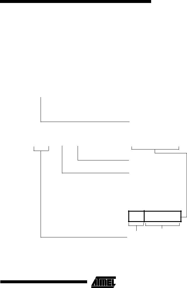
The MRS and MSR instructions are formed from a subset of the Data Processing operations and are implemented using the TEQ, TST, CMN and CMP instructions without the S flag set. The encoding is shown in Figure 20.
These instructions allow access to the CPSR and SPSR registers. The MRS instruction allows the contents of the CPSR or SPSR_<mode> to be moved to a general register. The MSR instruction allows the contents of a general register to be moved to the CPSR or SPSR_<mode> register.
The MSR instruction also allows an immediate value or register contents to be transferred to the condition code flags (N,Z,C and V) of CPSR or SPSR_<mode> without affecting the control bits. In this case, the top four bits of the specified register contents or 32 bit immediate value are written to the top four bits of the relevant PSR.
Operand restrictions
•In User mode, the control bits of the CPSR are protected from change, so only the condition code flags of the CPSR can be changed. In other (privileged) modes the entire CPSR can be changed.
•Note that the software must never change the state of the T bit in the CPSR. If this happens, the processor will enter an unpredictable state.
•The SPSR register which is accessed depends on the mode at the time of execution. For example, only SPSR_fiq is accessible when the processor is in FIQ mode.
•You must not specify R15 as the source or destination register.
•Also, do not attempt to access an SPSR in User mode, since no such register exists.
40 Instruction Set

Instruction Set
Figure 20. PSR Transfer
MRS (transfer PSR contents to a register)
31 28 27 23 22 21 16 15 12 11 0
|
|
|
Cond |
|
00010 |
|
P |
001111 |
|
|
Rd |
|
|
000000000000 |
|
|
|
|
|||||||||
|
|
|
|
|
|
|
|
|
|
s |
|
|
|
|
|
|
|
|
|
|
|
|
|
|
|
|
|
|
|
|
|
|
|
|
|
|
|
|
|
|
|
|
|
|
|
|
Destination register |
||||||||
|
|
|
|
|
|
|
|
|
|
|
|
|
|
|
|
|
|
|
|||||||||
|
|
|
|
|
|
|
|
|
|
|
|
|
|
|
|
|
|
|
|||||||||
|
|
|
|
|
|
|
|
|
|
|
|
|
|
|
|
|
|
|
Source PSR |
|
|
|
|
|
|
||
|
|
|
|
|
|
|
|
|
|
|
|
|
|
|
|
|
|
|
|
|
|
|
|
|
|||
|
|
|
|
|
|
|
|
|
|
|
|
|
|
|
|
|
|
|
|
0=CPSR |
|
|
|
|
|
|
|
|
|
|
|
|
|
|
|
|
|
|
|
|
|
|
|
|
|
|
|
1=SPSR_<current mode> |
|||||||
|
|
|
|
|
|
|
|
|
|
|
|
|
|
|
|
|
|
|
Condition field |
|
|
|
|
|
|
||
|
|
|
|
MSR (transfer register contents to PSR) |
|
|
|
|
|
|
|
|
|
|
|||||||||||||
|
|
|
|
|
|
|
|
|
|
|
|
|
|
|
|
|
|||||||||||
31 |
28 |
27 |
23 |
22 |
|
21 |
|
|
|
|
|
12 |
11 |
4 |
|
3 |
0 |
||||||||||
|
|
|
|
|
|
|
|
|
|
|
|
|
|
|
|
|
|
|
|
|
|
|
|
|
|
|
|
|
|
Cond |
|
00010 |
P |
1010011111 |
|
|
|
|
|
00000000 |
|
|
|
Rm |
|||||||||||
|
|
|
|
|
|
|
|
|
|
d |
|
|
|
|
|
|
|
|
|
|
|
|
|
|
|
|
|
|
|
|
|
|
|
|
|
|
|
|
|
|
|
|
|
|
|
|
|
|
|
|
|
|
|
|
|
|
|
|
|
|
|
|
|
|
|
|
|
|
|
|
|
|
|
|
|
|
|
|
|
|
|
|
|
|
|
|
|
|
|
|
|
|
|
|
|
|
|
|
|
|
|
|
Source register |
|
|
|
|
|
|
||
|
|
|
|
|
|
|
|
|
|
|
|
|
|
|
|
|
|
|
|
|
|
|
|
|
|||
|
|
|
|
|
|
|
|
|
|
|
|
|
|
|
|
|
|
|
Destination PSR |
|
|
|
|
|
|
||
|
|
|
|
|
|
|
|
|
|
|
|
|
|
|
|
|
|
|
|
|
|
|
|
|
|||
|
|
|
|
|
|
|
|
|
|
|
|
|
|
|
|
|
|
|
|
0=CPSR |
|
|
|
|
|
|
|
|
|
|
|
|
|
|
|
|
|
|
|
|
|
|
|
|
|
|
|
1=SPSR_<current mode> |
Condition field
MSR (transfer register contents or immdiate value to PSR flag bits only)
31 |
28 |
27 |
|
23 22 |
21 |
12 |
11 |
0 |
|
|
|
|
|
|
|
|
|
|
|
Cond |
|
00 |
I |
10 |
Pd |
|
1010001111 |
|
Source operand |
|
|
|
|
|
|
|
|
|
|
Destination PSR
0=CPSR 1=SPSR_<current mode>
Immediate Operand
11 |
0=source operand is a register |
0 |
|
||||||
|
|
4 |
3 |
|
|
||||
|
|
|
|
|
|
|
|
|
|
|
00000000 |
|
|
Rm |
|
|
|
||
|
|
|
|
|
|||||
|
|
|
|
|
|
|
|
|
|
|
|
|
|
|
|
|
|
||
|
|
|
|
|
|
|
|
|
|
|
|
|
|
|
|
|
|||
|
|
|
|
|
Source register |
||||
|
1=source operand is an immediate value |
||||||||
11 |
8 |
7 |
|
|
|
|
0 |
|
|
Rotate Imm
Unsigned 8 bit immediate value shift applied to Imm
Condition field
41

Reserved bits
Only twelve bits of the PSR are defined in ARM7TDMI (N,Z,C,V,I,F, T & M[4:0]); the remaining bits are reserved for use in future versions of the processor. Refer to Figure 9 for a full description of the PSR bits.
To ensure the maximum compatibility between ARM7TDMI programs and future processors, the following rules should be observed:
•The reserved bits should be preserved when changing the value in a PSR.
•Programs should not rely on specific values from the reserved bits when checking the PSR status, since they may read as one or zero in future processors.
Example
The following sequence performs a mode change:
A read-modify-write strategy should therefore be used when altering the control bits of any PSR register; this involves transferring the appropriate PSR register to a general register using the MRS instruction, changing only the relevant bits and then transferring the modified value back to the PSR register using the MSR instruction.
MRS |
R0,CPSR |
; Take a |
copy of |
the CPSR. |
||
BIC |
R0,R0,#0x1F |
; Clear the mode bits. |
||||
ORR |
R0,R0,#new_mode |
; Select |
new |
mode |
|
|
MSR |
CPSR,R0 |
; |
Write back |
the modified |
||
|
|
; |
CPSR. |
|
|
|
When the aim is simply to change the condition code flags in a PSR, a value can be written directly to the flag bits without disturbing the control bits. The following instruction sets the N,Z,C and V flags:
MSR |
CPSR_flg,#0xF0000000 |
; Set all the flags |
||
|
|
; regardless |
of their |
|
|
|
; |
previous state (does not |
|
|
|
; |
affect any |
control bits). |
No attempt should be made to write an 8 bit immediate value into the whole PSR since such an operation cannot preserve the reserved bits.
Instruction cycle times
PSR Transfers take 1S incremental cycles, where S is as defined in Cycle Types.
42 Instruction Set

Assembler syntax
1. MRS - transfer PSR contents to a register
MRS{cond} Rd,<psr>
2. MSR - transfer register contents to PSR
MSR{cond} <psr>,Rm
3.MSR - transfer register contents to PSR flag bits only
MSR{cond} <psrf>,Rm
The most significant four bits of the register contents are written to the N,Z,C & V flags respectively.
4.MSR - transfer immediate value to PSR flag bits only
MSR{cond} <psrf>,<#expression>
The expression should symbolise a 32 bit value of which the most significant four bits are written to the N,Z,C and V flags respectively.
Instruction Set
Key:
{cond} two-character condition mnemonic. See Table 6.
Rd and Rm are expressions evaluating to a register number other than R15
<psr> is CPSR, CPSR_all, SPSR or SPSR_all. (CPSR and CPSR_all are synonyms as are SPSR and SPSR_all)
<psrf> is CPSR_flg or SPSR_flg
<#expression>where this is used, the assembler will attempt to generate a shifted immediate 8-bit field to match the expression. If this is impossible, it will give an error.
Examples
In User mode the instructions behave as follows:
MSR |
CPSR_all,Rm |
; CPSR[31:28] |
<- |
Rm[31:28] |
||
MSR |
CPSR_flg,Rm |
; |
CPSR[31:28] |
<- |
Rm[31:28] |
|
MSR |
CPSR_flg,#0xA0000000; CPSR[31:28] <- 0xA |
|||||
|
|
;(set N,C; |
clear |
Z,V) |
||
MRS |
Rd,CPSR |
; |
Rd[31:0] |
<- |
CPSR[31:0] |
In privileged modes the instructions behave as follows:
MSR |
CPSR_all,Rm |
; CPSR[31:0] |
<- |
Rm[31:0] |
|
MSR |
CPSR_flg,Rm |
; CPSR[31:28] |
<- |
Rm[31:28] |
|
MSR |
CPSR_flg,#0x50000000; CPSR[31:28] <- 0x5 |
||||
|
|
;(set Z,V; |
clear |
N,C) |
|
MRS |
Rd,CPSR |
; Rd[31:0] |
<- |
CPSR[31:0] |
|
MSR |
SPSR_all,Rm |
;SPSR_<mode>[31:0]<- Rm[31:0] |
|||
MSR |
SPSR_flg,Rm |
; SPSR_<mode>[31:28] <- Rm[31:28] |
|||
MSR |
SPSR_flg,#0xC0000000; SPSR_<mode>[31:28] <- 0xC |
||||
|
|
;(set N,Z; |
clear |
C,V) |
|
MRS |
Rd,SPSR |
; Rd[31:0] |
<- |
SPSR_<mode>[31:0] |
43