
- •Introduction
- •ARM7TDMI Architecture
- •The THUMB Concept
- •THUMB’s Advantages
- •ARM7TDMI Block Diagram
- •ARM7TDMI Core Diagram
- •ARM7TDMI Functional Diagram
- •Key to signal types
- •Processor Operating States
- •Switching State
- •Entering THUMB state
- •Entering ARM state
- •Memory Formats
- •Big endian format
- •Little endian format
- •Instruction Length
- •Data Types
- •Operating Modes
- •Registers
- •The ARM state register set
- •The THUMB state register set
- •The relationship between ARM and THUMB state registers
- •Accessing Hi registers in THUMB state
- •The Program Status Registers
- •The condition code flags
- •The control bits
- •Exceptions
- •Action on entering an exception
- •Action on leaving an exception
- •Exception entry/exit summary
- •Notes
- •Abort
- •Software interrupt
- •Undefined instruction
- •Exception vectors
- •Exception priorities
- •Not all exceptions can occur at once:
- •Interrupt Latencies
- •Reset
- •Instruction Set Summary
- •Format summary
- •Instruction summary
- •The Condition Field
- •Branch and Exchange (BX)
- •Instruction cycle times
- •Assembler syntax
- •Using R15 as an operand
- •Examples
- •Branch and Branch with Link (B, BL)
- •The link bit
- •Instruction cycle times
- •Assembler syntax
- •Examples
- •Data Processing
- •CPSR flags
- •Shifts
- •Instruction specified shift amount
- •Register specified shift amount
- •Immediate operand rotates
- •Writing to R15
- •Using R15 as an operand
- •TEQ, TST, CMP and CMN opcodes
- •Instruction cycle times
- •Assembler syntax
- •where:
- •Examples
- •PSR Transfer (MRS, MSR)
- •Operand restrictions
- •Reserved bits
- •Example
- •Instruction cycle times
- •Assembler syntax
- •Examples
- •Multiply and Multiply-Accumulate (MUL, MLA)
- •If the operands are interpreted as signed
- •If the operands are interpreted as unsigned
- •Operand restrictions
- •CPSR flags
- •Instruction cycle times
- •Assembler syntax
- •Examples
- •Multiply Long and Multiply-Accumulate Long (MULL,MLAL)
- •Operand restrictions
- •CPSR flags
- •Instruction cycle times
- •For signed instructions SMULL, SMLAL:
- •For unsigned instructions UMULL, UMLAL:
- •Assembler syntax
- •where:
- •Examples
- •Single Data Transfer (LDR, STR)
- •Offsets and auto-indexing
- •Shifted register offset
- •Bytes and words
- •Little endian configuration
- •Big endian configuration
- •Restriction on the use of base register
- •Example:
- •Data aborts
- •Instruction cycle times
- •Assembler syntax
- •Examples
- •Halfword and Signed Data Transfer(LDRH/STRH/LDRSB/LDRSH)
- •Offsets and auto-indexing
- •Halfword load and stores
- •Signed byte and halfword loads
- •Endianness and byte/halfword selection
- •Little endian configuration
- •Big endian configuration
- •Data aborts
- •Instruction cycle times
- •Assembler syntax
- •Examples
- •Block Data Transfer (LDM, STM)
- •The register list
- •Addressing modes
- •Address alignment
- •LDM with R15 in transfer list and S bit set (Mode changes)
- •STM with R15 in transfer list and S bit set (User bank transfer)
- •R15 not in list and S bit set (User bank transfer)
- •Use of R15 as the base
- •Inclusion of the base in the register list
- •Data aborts
- •Aborts during STM instructions
- •Aborts during LDM instructions
- •Instruction cycle times
- •Assembler syntax
- •Addressing mode names
- •Examples
- •Single Data Swap (SWP)
- •Bytes and words
- •Data aborts
- •Instruction cycle times
- •Assembler syntax
- •Examples
- •Software Interrupt (SWI)
- •Return from the supervisor
- •Comment field
- •Instruction cycle times
- •Assembler syntax
- •Examples
- •Supervisor code
- •Coprocessor Data Operations (CDP)
- •The coprocessor fields
- •Instruction cycle times
- •Assembler syntax
- •Examples
- •Coprocessor Data Transfers (LDC, STC)
- •The coprocessor fields
- •Addressing modes
- •Address alignment
- •Data aborts
- •Instruction cycle times
- •Assembler syntax
- •Examples
- •Coprocessor Register Transfers (MRC, MCR)
- •The coprocessor fields
- •Transfers to R15
- •Transfers from R15
- •Instruction cycle times
- •Assembler syntax
- •Examples
- •Undefined Instruction
- •Instruction cycle times
- •Assembler syntax
- •Instruction Set Examples
- •Using the conditional instructions
- •Using conditionals for logical OR
- •Absolute value
- •Multiplication by 4, 5 or 6 (run time)
- •Combining discrete and range tests
- •Division and remainder
- •Overflow detection in the ARM7TDMI
- •Pseudo-random binary sequence generator
- •Multiplication by constant using the barrel shifter
- •Multiplication by 2^n (1,2,4,8,16,32..)
- •Multiplication by 2^n+1 (3,5,9,17..)
- •Multiplication by 2^n-1 (3,7,15..)
- •Multiplication by 6
- •Multiply by 10 and add in extra number
- •General recursive method for Rb := Ra*C, C a constant:
- •Loading a word from an unknown alignment
- •Format Summary
- •Opcode Summary
- •Format 1: move shifted register
- •Operation
- •Instruction cycle times
- •Examples
- •Format 2: add/subtract
- •Operation
- •Instruction cycle times
- •Examples
- •Format 3: move/compare/add/subtract immediate
- •Operations
- •Instruction cycle times
- •Examples
- •Format 4: ALU operations
- •Operation
- •Instruction cycle times
- •Examples
- •Format 5: Hi register operations/branch exchange
- •Operation
- •Instruction cycle times
- •The BX instruction
- •Examples
- •Using R15 as an operand
- •Format 6: PC-relative load
- •Operation
- •Instruction cycle times
- •Examples
- •Format 7: load/store with register offset
- •Operation
- •Instruction cycle times
- •Examples
- •Format 8: load/store sign-extended byte/halfword
- •Operation
- •Instruction cycle times
- •Examples
- •Format 9: load/store with immediate offset
- •Operation
- •Instruction cycle times
- •Examples
- •Format 10: load/store halfword
- •Operation
- •Instruction cycle times
- •Examples
- •Format 11: SP-relative load/store
- •Operation
- •Instruction cycle times
- •Examples
- •Format 12: load address
- •Operation
- •Instruction cycle times
- •Examples
- •Format 13: add offset to Stack Pointer
- •Operation
- •Instruction cycle times
- •Examples
- •Format 14: push/pop registers
- •Operation
- •Instruction cycle times
- •Examples
- •Format 15: multiple load/store
- •Operation
- •Instruction cycle times
- •Examples
- •Format 16: conditional branch
- •Operation
- •Instruction cycle times
- •Examples
- •Format 17: software interrupt
- •Operation
- •Instruction cycle times
- •Examples
- •Format 18: unconditional branch
- •Operation
- •Examples
- •Format 19: long branch with link
- •Operation
- •Instruction cycle times
- •Examples
- •Instruction Set Examples
- •Multiplication by a constant using shifts and adds
- •General purpose signed divide
- •Thumb code
- •ARM code
- •Division by a constant
- •Explanation of divide-by-constant ARM code
- •ARM code
- •THUMB code
- •Overview
- •Cycle Types
- •Address Timing
- •Data Transfer Size
- •Instruction Fetch
- •Memory Management
- •Locked Operations
- •Stretching Access Times
- •The ARM Data Bus
- •The External Data Bus
- •The unidirectional data bus
- •The bidirectional data bus
- •Example system: The ARM7TDMI Testchip
- •Overview
- •Interface Signals
- •Coprocessor present/absent
- •Busy-waiting
- •Pipeline following
- •Data transfer cycles
- •Register Transfer Cycle
- •Privileged Instructions
- •Idempotency
- •Undefined Instructions
- •Debug Interface
- •Overview
- •Debug Systems
- •Debug Interface Signals
- •Entry into debug state
- •Entry into debug state on breakpoint
- •Entry into debug state on watchpoint
- •Entry into debug state on debug-request
- •Action of ARM7TDMI in debug state
- •Scan Chains and JTAG Interface
- •Scan limitations
- •Scan chain 0
- •Scan chain 1
- •Scan Chain 2
- •The JTAG state machine
- •Reset
- •Pullup Resistors
- •Instruction Register
- •Public Instructions
- •EXTEST (0000)
- •SCAN_N (0010)
- •INTEST (1100)
- •IDCODE (1110)
- •BYPASS (1111)
- •CLAMP (0101)
- •HIGHZ (0111)
- •CLAMPZ (1001)
- •SAMPLE/PRELOAD (0011)
- •RESTART (0100)
- •Test Data Registers
- •Bypass register
- •ARM7TDMI device identification (ID) code register
- •Operating mode:
- •Instruction register
- •Scan chain select register
- •Scan chains 0,1 and 2
- •Scan chain 0 and 1
- •Scan chain 0
- •Scan chain 1
- •Scan chain 3
- •ARM7TDMI Core Clocks
- •Clock switch during debug
- •Clock switch during test
- •Determining the Core and System State
- •Determining the core’s state
- •Determining system state
- •Exit from debug state
- •The PC’s Behaviour During Debug
- •Breakpoint
- •Watchpoints
- •Watchpoint with another exception
- •Debug request
- •System speed access
- •Summary of return address calculations
- •Priorities / Exceptions
- •Breakpoint with prefetch abort
- •Interrupts
- •Data aborts
- •Scan Interface Timing
- •Debug Timing
- •Overview
- •The Watchpoint Registers
- •Programming and reading watchpoint registers
- •Using the mask registers
- •The control registers
- •Programming Breakpoints
- •Hardware breakpoints:
- •Software breakpoints:
- •Hardware breakpoints
- •Software breakpoints
- •Setting the breakpoint
- •Clearing the breakpoint
- •Programming Watchpoints
- •The Debug Control Register
- •Debug Status Register
- •Coupling Breakpoints and Watchpoints
- •Example
- •CHAINOUT signal
- •RANGEOUT signal
- •Example
- •Disabling ICEBreaker
- •ICEBreaker Timing
- •Programming Restriction
- •Debug Communications Channel
- •Debug comms channel registers
- •Communications via the comms channel
- •Introduction
- •Branch and Branch with Link
- •THUMB Branch with Link
- •Branch and Exchange (BX)
- •Data Operations
- •Multiply and Multiply Accumulate
- •Load Register
- •Store Register
- •Load Multiple Registers
- •Store Multiple Registers
- •Data Swap
- •Software Interrupt and Exception Entry
- •Coprocessor Data Operation
- •Coprocessor Data Transfer (from memory to coprocessor)
- •Coprocessor Data Transfer (from coprocessor to memory)
- •Coprocessor Register Transfer (Load from coprocessor)
- •Coprocessor Register Transfer (Store to coprocessor)
- •Undefined Instructions and Coprocessor Absent
- •Unexecuted Instructions
- •Instruction Speed Summary
- •Timing Diagrams

Instruction Set
CPSR flags
The data processing operations may be classified as logical or arithmetic. The logical operations (AND, EOR, TST, TEQ, ORR, MOV, BIC, MVN) perform the logical action on all corresponding bits of the operand or operands to produce the result. If the S bit is set (and Rd is not R15, see
below) the V flag in the CPSR will be unaffected, the C flag will be set to the carry out from the barrel shifter (or preserved when the shift operation is LSL #0), the Z flag will be set if and only if the result is all zeros, and the N flag will be set to the logical value of bit 31 of the result.
Table 7. ARM Data Processing Instructions
Assembler Mnemonic |
OpCode |
Action |
|
|
|
|
|
|
|
AND |
0000 |
operand1 AND operand2 |
|
|
EOR |
0001 |
operand1 EOR operand2 |
|
|
SUB |
0010 |
operand1 - operand2 |
|
|
RSB |
0011 |
operand2 - operand1 |
|
|
ADD |
0100 |
operand1 + operand2 |
|
|
ADC |
0101 |
operand1 + operand2 + carry |
|
|
SBC |
0110 |
operand1 - operand2 + carry - 1 |
|
|
RSC |
0111 |
operand2 - operand1 + carry - 1 |
|
|
TST |
1000 |
as AND, but result is not written |
|
|
TEQ |
1001 |
as EOR, but result is not written |
|
|
CMP |
1010 |
as SUB, but result is not written |
|
|
CMN |
1011 |
as ADD, but result is not written |
|
|
ORR |
1100 |
operand1 OR operand2 |
|
|
MOV |
1101 |
operand2 |
(operand1 is ignored) |
|
BIC |
1110 |
operand1 AND NOT operand2 |
(Bit clear) |
|
MVN |
1111 |
NOT operand2 |
(operand1 is ignored) |
The arithmetic operations (SUB, RSB, ADD, ADC, SBC, RSC, CMP, CMN) treat each operand as a 32 bit integer (either unsigned or 2’s complement signed, the two are equivalent). If the S bit is set (and Rd is not R15) the V flag in the CPSR will be set if an overflow occurs into bit 31 of the result; this may be ignored if the operands were considered unsigned, but warns of a possible error if the operands were 2’s complement signed. The C flag will be set to the carry out of bit 31 of the ALU, the Z flag will be set if and only if the result was zero, and the N flag will be set to the value of bit 31 of the result (indicating a negative result if the operands are considered to be 2’s complement signed).
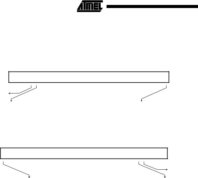
Shifts
When the second operand is specified to be a shifted register, the operation of the barrel shifter is controlled by the Shift field in the instruction. This field indicates the type of shift to be performed (logical left or right, arithmetic right or rotate right). The amount by which the register should be shifted may be contained in an immediate field in the instruction, or in the bottom byte of another register (other than R15). The encoding for the different shift types is shown in Figure 14.
Figure 14. ARM Shift Operations
11 |
7 |
6 |
5 |
4 |
|
|
11 |
|
8 |
7 |
6 |
5 |
4 |
|
|
|||||||
|
|
|
|
|
|
|
|
0 |
|
|
|
Rs |
|
0 |
|
|
|
|
1 |
|
|
|
|
|
|
|
|
|
|
|
|
|
|
|
|
|
|
|
|
|
|
|
|
||
|
|
|
|
|
|
|
|
|
Shift type |
|
|
|
|
|
|
|
|
|
|
Shift type |
||
|
|
|
|
|
|
|
|
|
|
|
|
|
|
|
|
|
|
|
||||
|
|
|
|
|
|
|
|
|
|
|
|
|
|
|
|
|
|
|
||||
|
|
|
|
|
|
|
|
|
|
|
|
|
|
|
|
|
||||||
|
|
|
|
|
|
|
|
00 |
= logical left |
|
|
|
|
|
|
|
|
|
00 |
= logical left |
||
|
|
|
|
|
|
|
|
01 |
= logical right |
|
|
|
|
|
|
|
|
|
01 |
= logical right |
||
|
|
|
|
|
|
|
|
10 |
= arithmetic right |
|
|
|
|
|
|
|
|
|
10 |
= arithmetic right |
||
|
|
|
|
|
|
|
|
11 |
= rotate right |
|
|
|
|
|
|
|
|
|
11 |
= rotate right |
||
|
|
|
|
|
|
|
|
|
Shift amount |
|
|
|
|
|
|
|
|
|
|
Shift register |
||
|
|
|
|
|
|
|
|
|
|
|
|
|
|
|
|
|
||||||
|
|
|
|
|
|
|
|
|
5 bit unsigned integer |
|
|
|
|
|
|
|
|
|
|
Shift amount specified in |
||
|
|
|
|
|
|
|
|
|
|
|
|
|
|
|
|
|
|
|
|
|
bottom byte of Rs |
35

Instruction specified shift amount
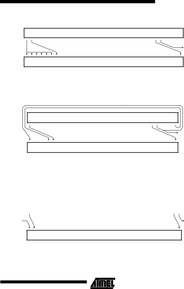
When the shift amount is specified in the instruction, it is contained in a 5 bit field which may take any value from 0 to 31. A logical shift left (LSL) takes the contents of Rm and moves each bit by the specified amount to a more significant position. The least significant bits of the result are filled with zeros, and the high bits of Rm which do not map into the
Figure 15. Logical Shift Left
31 |
27 |
26 |
result are discarded, except that the least significant discarded bit becomes the shifter carry output which may be latched into the C bit of the CPSR when the ALU operation is in the logical class (see above). For example, the effect of LSL #5 is shown in Figure 15.
0
contents of Rm
carry out
value of operand 2 |
0 0 0 0 0 |
|
|
Note: LSL #0 is a special case, where the shifter carry out is the old value of the CPSR C flag. The contents of Rm are used directly as the second operand.
Figure 16. Logical Shift Right
A logical shift right (LSR) is similar, but the contents of Rm are moved to less significant positions in the result. LSR #5 has the effect shown in Figure 16.
31 |
5 |
4 |
0 |
contents of Rm
carry out
0 0 0 0 0 |
value of operand 2 |
|
|
The form of the shift field which might be expected to correspond to LSR #0 is used to encode LSR #32, which has a zero result with bit 31 of Rm as the carry output. Logical shift right zero is redundant as it is the same as logical shift left zero, so the assembler will convert LSR #0 (and ASR #0 and ROR #0) into LSL #0, and allow LSR #32 to be specified.
An arithmetic shift right (ASR) is similar to logical shift right, except that the high bits are filled with bit 31 of Rm instead of zeros. This preserves the sign in 2’s complement notation. For example, ASR #5 is shown in Figure 17.
36 Instruction Set

Instruction Set
Figure 17. Arithmetic Shift Right
31 |
30 |
5 |
4 |
0 |
contents of Rm
carry out
value of operand 2
The form of the shift field which might be expected to give ASR #0 is used to encode ASR #32. Bit 31 of Rm is again used as the carry output, and each bit of operand 2 is also equal to bit 31 of Rm. The result is therefore all ones or all zeros, according to the value of bit 31 of Rm.
Figure 18. Rotate Right
31
Rotate right (ROR) operations reuse the bits which “overshoot” in a logical shift right operation by reintroducing them at the high end of the result, in place of the zeros used to fill the high end in logical right operations. For example, ROR #5 is shown in Figure 18.
5 |
4 |
0 |
contents of Rm
carry out
value of operand 2
The form of the shift field which might be expected to give ROR #0 is used to encode a special function of the barrel shifter, rotate right extended (RRX). This is a rotate right by
one bit position of the 33 bit quantity formed by appending the CPSR C flag to the most significant end of the contents of Rm as shown in Figure 19.
Figure 19. Rotate Right Extended
31 |
1 |
0 |
|
|
|
|
contents of Rm |
|
|
|
|
|
|
|
C |
|
|
carry |
|
in |
|
|
out |
value of operand 2
Register specified shift amount
Only the least significant byte of the contents of Rs is used to determine the shift amount. Rs can be any general register other than R15.
If this byte is zero, the unchanged contents of Rm will be used as the second operand, and the old value of the CPSR C flag will be passed on as the shifter carry output.
37