

5.5.2Simulation and prototype testing
Because of the variations in the types of ICs, and the applications they find themselves in, some engineers will find these rules of thumb not tough enough, and some will wonder whether they are over-engineered, but that is the function of a rule of thumb, after all.
Computer-based circuit simulation techniques that calculate EMC and / or signal integrity based on parameters extracted from an actual PCB layout are becoming more capable, and their use is recommended instead of the crude rules-of-thumb expressed here. However, remember that device switching speed are almost always considerably faster than their data sheet specifications, so a simulation that uses data sheet figures will give a false sense of confidence.
Tests with a high-speed oscilloscope and probing system should be carried out on the first PCB prototypes to see whether the waveshape is good enough. A waveshape that does not distort as it travels around the PCB is the goal, and merely following these rules of thumb is unlikely to achieve such perfection, although the result may be good enough. Close-field probing with a single-turn loop, using a high-speed ‘scope and/or a spectrum analyser, is another good way to detect signal integrity or EMC problems at prototype board level. The techniques involved in prototype testing are not discussed further here.
Even when using sophisticated modelling or simulation techniques, always perform signal integrity and EMC checks on early prototypes.
5.5.3Manufacturing issues with transmission lines
Normal FR4 PCB material has a nominal relative dielectric constant (εr) of approximately 4.7 at 1MHz falling roughly in a linear fashion with increasing frequency to 4.2 at 1GHz. Actual values of εr, can vary by ±25%. Controlled εr grades of FR4 are available at little or no extra cost, but PCB manufacturers may not use these grades unless specifically requested.
PCB manufacturers work with standard thickness laminations (“prepregs”), and their thicknesses should be discovered (along with their manufacturing tolerances) before design starts. The track widths can then be chosen to achieve the required Z0 for the available range of dielectric thicknesses. Track widths after PCB processing are usually about one thousandth of an inch less than those used on the photoplots. Ask what thickness to add to the drawn tracks to achieve the required finished track widths.
For signal frequencies greater than 1GHz it may be necessary to use other dielectric materials than FR4, such as those used for microwave applications (e.g. Duroid from Rogers Corporation Inc., or a number of more modern dielectrics).
5.5.4Terminating transmission lines
“Classical” RF transmission lines are terminated both at signal source and load by impedances equal to their Z0 (allowing for the internal impedances of source and load devices). Although an ideal and sometimes necessary technique, it halves the received voltage – so most ordinary analogue and digital circuits use low-Z sources and high-Z loads with the line only terminated at one end, to preserve signal levels.
RF engineers often use reactive components or even lengths of track as line terminations, but the terminations for wideband analogue and conventional digital signals require individual resistors, preferably SMD types for their excellent high-frequency performance. To get the best from SMD resistors they must be connected to the reference planes using low inductance techniques as shown by figure 5C.
Figure 5H shows the common termination techniques. Classical RF termination is still often used for high-speed signals such as fast backplane systems.
Design techniques for EMC– Part 5: PCBs |
Cherry Clough Consultants Feb 2000 Page 19 of 24 |
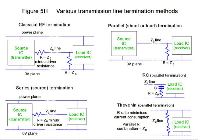
Where signals are restricted to a single PCB, series (source) termination may be used at the driver end of a transmission line, with the resistor chosen so that in series with the impedance of the output driver it matches the line’s Z0. This method has the advantage of consuming little power, and is most suitable for lines with a single load device at their far end. Where other loads exist along the length of the line they experience "reflected wave switching" and their response may need to be slowed to prevent false clocking.
Parallel (shunt, or load) termination at the very far end of a line is used where there are a number of devices spread along the length of the line and they need to respond most quickly, and achieves “incident wave switching”. Figure 5H shows the termination resistor connected to the 0V plane, but some logic families use other reference voltages (e.g. the positive plane for ECL). Parallel termination dissipates a lot of power, and may also load some IC outputs too heavily.
Alternative types of parallel termination include "Thévenin" and RC. Thévenin uses resistor values designed so that their parallel resistance is Z0 and they would provide a DC voltage at their junction equal to the average line voltage, to minimise power dissipation. Thévenin termination needs a properly decoupled power plane at all frequencies of concern so needs decoupling capacitors nearby. RC termination uses capacitor values between 10 and 620pF (typically) and only terminates the line for high frequencies. Because of the problems of capacitors (discussed earlier) it may be more difficult for an RC termination to equal the highest frequency performance of a parallel resistor or Thévenin termination.
"Active termination" uses a voltage regulator to drive an additional power plane at the nominal average value of the digital signals. A parallel line termination connects to this plane, which must be properly decoupled for the frequencies of concern. Electrically equivalent to the Thévenin method, this can save power by running the voltage regulator (which needs to be able to source as well as sink current) in Class AB.
Design techniques for EMC– Part 5: PCBs |
Cherry Clough Consultants Feb 2000 Page 20 of 24 |
Where a line is driven bi-directionally the compromise position for terminating resistors (series or parallel) is in the centre of the line, so such lines should always be kept very short and may not be able to run as fast as the device speeds may suggest. Series terminations at all possible drivers may be used instead of series termination at the centre of the line, but this may not give good signal integrity unless all the lines concerned are very short. Parallel termination at both ends of the line can give very good performance and allows the highest data rates, but drivers must capable of driving the resulting lower impedances, and power dissipation will also increase. Parallel (or Thévenin or active) termination at both ends is used for serial or parallel data cables such as SCSI and Ethernet.
When “star” connecting a number of individual series-terminated transmission lines, either use one termination resistor chosen so that the total source resistance equals the parallel combination of all the starred lines, or else use one resistor to match each line. The latter technique should be better. The star configuration may also be used to drive multiple parallel-terminated lines. In either case, the signal source must be capable of driving the parallel combination of all the lines' Z0s.
It is generally better to choose higher values of Z0 to reduce signal currents and reduce radiation from the tracks. Many ordinary CMOS or TTL ICs were never designed for driving transmission lines, and have neither the drive capability or an output impedance that is equal for both sourcing and sinking. Such devices may be able to use series, Thevenin, RC, or active terminations on highimpedance lines, but the best method to use, and the line impedance, may be difficult to predict for a given logic family.
However, an increasing number of devices are becoming available to drive transmission lines, and the increasing range of LVDS and similar devices is making clock and bus driving much easier and easing EMC problems. Backplane bus driver ICs are available with 25Ω output impedances, suitable for “star” driving four individual 100Ω, or six 150Ω lines. Some devices now have on-chip DC/DC converters which cause their unloaded outputs to achieve double the correct logic levels, so that when operated into a classically terminated line the received logic levels are correct.
5.5.5Layer "stack up"
The above section on decoupling shows it is good EMC practice to provide 0V and power planes on adjacent layers and to maximise their capacitance by using a thin dielectric (say 0.15mm) between them. The above section on transmission lines shows that proximity to a reference plane is important for high-speed tracks. We can put this all together to decide how to stack up our PCB layers.
Four-layer PCBs often have their layers stacked as follows:
1)Microstrip transmission lines and other critical signals
2)0V plane
3)+5V plane
4)Non-critical signals
Where more signal layers are required, a 0V and power plane "core" should be retained. Additional layers of high-speed signals may need additional 0V planes to be added, but high-speed clocks and data busses and similarly aggressive or very critical tracks should not swap layers.
Here is one of a number of possible stack-ups for an 8-layer computer motherboard:
1)0Vplane
2)Most critical “offset striplines” and other signals, routed at 90o to layer 3) to reduce crosstalk
3)Most critical “offset striplines” and other signals, routed at 90o to layer 2) to reduce crosstalk
4)0V plane
5)+5V plane
6)Non-critical signals routed at right angles to layer 7) to reduce crosstalk
7)Less critical “offset striplines” and other signals, routed at 90o to layer 6) to reduce crosstalk
8)0V plane
Design techniques for EMC– Part 5: PCBs |
Cherry Clough Consultants Feb 2000 Page 21 of 24 |
5.5.6Joints, stubs, and buffers
The above has treated transmission lines as if they were all point-to-point connections, so we need to address bussed systems such as RAM arrays, and situations where several cards interconnect at high speeds, such as backplane systems.
A length of track that springs off from a joint with the main track is called a ‘stub’. For memory arrays, the usual PCB layout technique is to route busses horizontally on one layer, ‘via-d’ through to another layer with vertically routed stubs to connect to the array devices. To preserve the transmission line the electrical length of the stubs must be kept to under one-eighth of the rise time (and preferably much less). Don’t forget that the important parameter is the real switching rate of the signals, not the data sheet specification of the drivers. If in doubt, assume the drivers switch four time faster than their data sheet maxima.
The stub length used for the calculation should include the distance from the end of the track (the IC’s soldered pin) to the centre of the IC itself. Where the permissible stub length is too short for traditional ‘horizontal and vertical’ array routing, daisy chain tracking should be used instead. Daisy chain tracking is generally better for high-speed signals in any case, especially when the tracks remain all on one layer. Daisy chain tracking means that the bussed tracks go from the source directly to each load in turn. Abrupt changes in track direction should be avoided, with gentle curves or large chamfers used instead. In an incident wave system, the daisy-chained tracks would end in the parallel, Thevenin, RC, or active termination resistors.
When electrically long stubs can’t be avoided, buffers should be fitted close to the main track to minimise the stub lengths. This is often used in backplane systems, where a number of plug-in cards must all run from the same clock lines and data busses, as shown in Figure 5J. The clock buffers must all be fitted very close to the backplane board connectors, and as signal speeds and data rates increase it is more common to find that matched-impedance backplane connectors are needed. Where a plug-in card only has one or two ICs that need to connect to the backplane clock and data lines, by placing them close the backplane connector it may be possible to do without the buffers.
Design techniques for EMC– Part 5: PCBs |
Cherry Clough Consultants Feb 2000 Page 22 of 24 |