

4.13Failing conducted tests due to inadequate shielding
Just because radiated phenomena are generally only tested above 30MHz, does not mean that shielding is unimportant below 30MHz. An enclosure that leaks excessively at low frequencies can cause a failure on a conducted test.
Small products with dimensions less than 0.5 metres usually make relatively inefficient antenna below 30MHz, and most problems are due to leaky cable screens (cables usually being long enough to be good antennae below 30 MHz). However, even a small product might need enclosure shielding that is effective at under 30MHz if it contains a powerful source of low-frequency fields.
4.14Installation of shielded enclosures
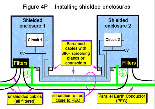
A wire poked through an aperture in a shielded enclosure will completely destroy any SE pretensions. Figure 4P shows the main aspects of how to install an shielded enclosure without ruining it.
The screens and connectors (or glands) of all screened cables that penetrate a shielded enclosure, and their 360º bonding, are as vital a part of any "Faraday Cage" as the enclosure metalwork itself. The thoughtful assembly and installation of filters for unshielded external cables is also vital to achieve a good SE. These points were made in Parts 2 and 3 of this series, and they are worth making again.
In passing it is worth repeating that a cable screen pigtailed to an enclosure shield (instead of being 360º bonded) will ruin the SE of that enclosure from quite low frequencies upwards (say, above 10MHz for a short pigtail, lower if it is longer).
Design techniques for EMC – Part 4 – Shielding |
Cherry Clough Consultants |
Page 20 of 23 |
Refer to the draft IEC1000-5-6 (95/210789 DC from BSI) for best practices in industrial cabinet shielding (and filtering) and BS IEC 61000-5-2:1998 for best practices in cabling (and earthing) – including why pigtails are best consigned to the history books along with soldering irons that had to be heated in a fire. Figure 4P shows the main points of installing shielded cabinets according to these two best-practice standards, and is repeated from part 2 of this series. Refer to Part 2 for more details on this figure as regards the installation of shielded cabling, and Part 3 for details of installing filters on unshielded cables.
4.15Using PCB-level shielding
Returning to our original theme of applying shielding at as low a level of assembly as possible to save costs, we should consider the issues of shielding at the level of the PCB.
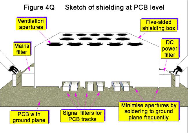
The ideal PCB-level shield is a totally enclosing metal box with shielded connectors and feedthrough filters mounted in its walls, really just a miniature version of a product-level shielded enclosure as described above. The result is often called a module, can provide extremely high SEs, and is very often used in the RF and microwave worlds.
Lower cost PCB shields are possible, although their SE is not usually as good as a well-designed module. All depend upon a ground plane in a PCB being used to provide one side of the shield, so that a simple five-sided box can be assembled on the PCB like any other component. Soldering this five-sided box to the ground plane at a number of points around its circumference creates a “Faraday cage” around the desired area of circuitry. A variety of standard five-sided PCB-mounted shielding boxes are readily available, and companies who specialise in this kind of precision metalwork often make custom designs. Boxes are available with snap-on lids so that adjustments may easily be made, test points accessed, or chips replaced, with the lid off. Such removable lids are usually fitted with spring-fingers all around their circumference to achieve a good SE when they are snapped in place.
Weak points in this method of shielding are obviously the apertures created by the gaps between the ground-plane soldered connections, by any apertures in the ground plane (e.g. clearances around through-leads and via holes), and any other apertures in the five-sided box (e.g. ventilation, access to adjustable components, displays, etc.). Seam-soldering the edges of a five-sided box to a component-side ground plane can remove one set of apertures, at the cost of a time-consuming manual operation.
For the lowest cost, we want to bring all our signals and power into the shielded area of our PCB as tracks, avoiding wires and cables. This means we need to use the PCB equivalents of bulkheadmounting shielded connectors, and bulkhead-mounting filters.
The PCB track equivalent of a shielded cable is a track run between two ground planes, often called a “stripline”. Sometimes guard tracks are run on both sides of this “shielded track” on the same copper layer, these guard tracks having very frequent via holes bonding them to the top and bottom ground planes. The number of via holes per inch is the limiting factor here, as the gaps between them act as shield apertures (the guard tracks have too much inductance on their own to provide a good SE at high-frequencies). Since the dielectric constant of the PCB material is roughly four times that of air, when figures 4F and 4G are used to determine via spacing their frequency axes should be divided by two (the square root of the PCB’s dielectric constant). Some designers don’t bother with the guard tracks and just use via holes to “channel” the track in question. It may be a good idea to randomly vary the spacings of such rows of via holes around the desired spacing, to help avoid resonances.
Where striplines enter an area of circuitry enclosed by a shielded box, it is sufficient that their upper and lower ground planes (and any guard tracks) are bonded to the screening can’s soldered joints on both sides, close to the stripline.
Track which only have a single ground plane layer in parallel, their other side being exposed to the air, are said to be of “microstrip” construction. When a microstrip enters a shielded PCB box it will suffer an impedance discontinuity due to the wall of the box. If the wavelength of the highest
Design techniques for EMC – Part 4 – Shielding |
Cherry Clough Consultants |
Page 21 of 23 |
frequency component of the signals in the microstrip is greater than 100 times the thickness of the box wall (or the width of box mounting flange), the discontinuity may be too brief to register. But where this is not the case some degradation in performance may occur, and such signals are best routed using striplines.
All unshielded tracks must be filtered as they enter a shielded PCB area. It is often possible to get valuable improvements using PCB shielding without such filtering, but this is difficult to predict so filtering should always be designed-in (at least on prototypes, only being removed from the PCB layout after successful EMC testing).
The best filters are feedthrough types, but to save cost we need to avoid wired types. Leaded PCBmounting types are available which can be soldered to a PCB in the usual manner and then handsoldered to the wall of the screening box when it is fitted at a later stage. Quicker assembly can be achieved by soldering the central contact of the filter to the underlying ground plane, making sure that solder joints between the shielding box and the same ground plane layer are close by, on both sides. This latter construction also suits surface-mounted “feedthrough” filters, further reducing assembly costs.
But feedthrough filters, even surface mounted types, are still more expensive than simple ferrite beads or capacitors. To allow the most cost-effective filters to be found during development EMC testing, whilst also minimising delay and avoiding PCB layout iterations, multipurpose pad patterns can easily be created to take any of the following filter configurations:
•zero-ohm link (no filtering, often used as the starting point when EMC testing a new design)
•a resistor or ferrite bead in series with the signal
•a capacitor to the ground plane
•common-mode chokes
•resistor/ferrite/capacitor combinations (tee, π, LC, etc. see Part 3 of this series for more details)
•feedthrough capacitor (i.e. centre-pin grounded, not truly feedthrough)
•feedthrough filter (tee, π, LC, etc., centre-pin grounded, not truly feedthrough)
Multipurpose padding also means we are not restricted to proprietary filters and can cook up our own to best suit the requirements of the circuit (and the product as a whole) at the lowest cost.
By now it should go without saying that all these PCB mounted filters should ideally be lined-up with their centres along the line of the wall of the shielding box, which will probably need a little cut-out in it to accommodate the components. Using surface-mounted devices rather than leaded allows the box cut-out size to be minimised, improving SE.
Where simple lines of filters are hard to achieve, take great care not to allow any unfiltered tracks to run close to any filtered tracks. Figure 4Q attempts to sketch what low-cost PCB shielding could look like.
Design techniques for EMC – Part 4 – Shielding |
Cherry Clough Consultants |
Page 22 of 23 |
As with cables, it may be necessary to use shielding and filtering together, so it may be a wise precaution to provide for multi-padded filter layouts for all the “shielded” tracks entering a shielded PCB area, or at least make provision for a ferrite bead.
4.16Further reading
EMC for Product Designers 3rd edition, by Tim Williams, Newnes 2001, ISBN: 0-7506-4930-5, www.newnespress.com
EMC for Systems and Installations, by Tim Williams and Keith Armstrong, Newnes 2000, ISBN 0 7506 4167 3 www.newnespress.com, RS Components Part No. 377-6463.
EMC for Systems and Installations Part 3 and Part 4, EMC+Compliance Journal, 2000. All UK EMC Journal and EMC+Compliance Journal articles are available electronically from the magazine’s archives at www.compliance-club.com
Eur Ing Keith Armstrong C.Eng MIEE MIEEE
Partner, Cherry Clough Consultants, Associate of EMC-UK, www.cherryclough.com Phone: 01457 871 605, Fax: 01457 820 145, Email: keith.armstrong@cherryclough.com
Design techniques for EMC – Part 4 – Shielding |
Cherry Clough Consultants |
Page 23 of 23 |