

04.Multiport circuit parameters and transmission lines
.pdf
|
|
|
|
COMMONLY USED TRANSMISSION LINES |
71 |
||||||
to Ez |
H2O. This energy is dissipated in the center and outer conductor. The |
||||||||||
O ð |
|
|
|
|
|
|
|
|
|
|
|
power loss per unit length is found in the following way: |
|
||||||||||
|
P$ D |
Rm |
|
Js Ð JsŁd$ |
|
|
|
|
|||
|
2 |
|
|
|
|
||||||
|
D |
Rm |
rˆ ð H Ð rˆ U H d$ |
|
|||||||
|
2 |
|
|||||||||
|
D |
Rm |
|
H Ð HŁd$ |
|
|
|
|
|||
|
2 |
|
|
|
|
||||||
|
|
RmV02, |
1 |
|
1 |
|
|
||||
|
D |
|
|
|
|
C |
|
|
4.99 |
||
|
+2 ln b/a 2 |
a |
b |
||||||||
The power, P, transmitted down the line is found by the Poynting theorem:
|
1 |
|
a |
b |
0 |
2, |
|
P D |
<fZmg |
|
E ð H Ð zOrdrd2 |
||||
|
|
||||||
2 |
|
||||||
|
|
,V2 |
|
|
|
|
|
D |
0 |
|
|
|
|
4.100 |
|
+ ln b/a |
|
|
|
|
|||
The attenuation constant associated with conductor loss is found from Eq. (4.95):
˛ |
P$ |
D |
|
Rm |
|
a C b |
4.101 |
|||
2P |
2+ ln b/a |
ab |
||||||||
c D |
|
|
||||||||
while the dielectric loss found earlier is |
|
|
|
|||||||
|
|
˛d D |
k0εr00 |
|
|
4.92 |
||||
|
|
2 |
|
|
|
|
||||
|
|
εr0 |
|
|
|
|||||
The total loss is found from Eq. (4.67).
4.7.4Microstrip Transmission Line
Microstrip has been a popular form of transmission line for RF and microwave frequencies for some time. The microstrip line shown in Fig. 4.18 consists of a conductor strip of width w on a dielectric of thickness h above a ground plane. Part of the electric field between the strip and the ground plane is in the dielectric and part in the air. The field is more concentrated in the dielectric than in the air. Consequently the effective dielectric constant, εeff, is somewhere between εr and 1, but closer to εr than 1. A variety of methods have been used to find εeff. However, rather than provide a proof, a simple empirically based procedure for synthesizing a microstrip line will be given. Microstrip line is not strictly a TEM type of transmission line and does have some frequency

72 MULTIPORT CIRCUIT PARAMETERS AND TRANSMISSION LINES
w
t
h
ε r
FIGURE 4.18 The microstrip transmission line.
dispersion. Unless microstrip is being used in a multi-octave frequency range application, the TEM approximation should be adequate. The synthesis problem occurs when the desired characteristic impedance, Z0, and the dielectric constant of the substrate, εr, are known and the geometrical quantity w/h is to be found. The synthesis equations, given by [4], are simple, and they give an approximate solution to the microstrip problem:
w |
|
8 |
11 |
|
7 C |
εr |
|
C |
0.81 |
1 C |
εr |
|
|
||||
|
|
|
|
|
|
A |
|
4 |
|
1 |
|
1 |
|
||||
|
|
D |
|
|
|
|
|
|
|
|
|
|
|
|
|
|
4.102 |
h |
|
|
|
|
p |
|
|
|
A |
|
|
|
|
||||
|
|
|
|
|
|
|
|
|
|
|
|
|
|
|
|
|
|
A |
D |
exp |
Z0 |
εr C 1 |
|
|
1 |
|
|
|
4.103 |
||||||
|
|
|
|
|
|||||||||||||
|
|
|
|
|
|
||||||||||||
|
|
|
|
|
|
42.4 |
|
|
|
|
|
|
|
|
|||
The analysis equations given below by [5] are more accurate than the synthesis equations. The value given by Eqs. (4.102) and (4.103) provides an initial value for w/h that can be used in an iterative procedure to successfully solve the synthesis problem. This process depends on knowing εr and the conductor thickness, t. The solution results in the effective dielectric constant, εeff, needed to determine electrical line lengths and Z0. The procedure for the analysis procedure is shown below:
ua D , |
ln 1 C t/h C coth2 p6.517w/h |
4.104 |
|||||||||||||||
|
|
t/h |
|
|
|
|
4 exp 1 |
|
|
|
|
||||||
|
|
|
1 C cosh pεr 1 |
|
|
|
|
|
|
|
|||||||
ur D |
2 |
|
ua |
|
|
|
4.105 |
||||||||||
|
|
1 |
|
|
|
|
|
1 |
|
|
|
|
|
|
|
|
|
ua D |
w |
C ua |
|
|
|
|
|
|
|
|
|
4.106 |
|||||
|
|
|
|
|
|
|
|
|
|
||||||||
h |
|
|
|
|
|
|
|
|
|
||||||||
ur D |
w |
C ur |
|
|
|
|
|
|
|
|
|
4.107 |
|||||
|
|
|
|
|
|
|
|
|
|
||||||||
h |
|
|
|
|
|
|
|
|
|
||||||||
Z0a x |
D |
2, ln |
x |
C |
|
|
|
|
|
4.108 |
|||||||
1 C x |
2 |
||||||||||||||||
|
|
+ |
|
|
f x |
|
|
|
2 |
|
|
|
|
|
|||
|
|
|
|
|
|
|
|
|
|
|
|
|
|
|
|
||
f x |
D 6 C 2, 6 |
exp[ 30.666/x 0.7528] |
4.109 |
||||||||||||||

|
|
|
|
|
|
|
|
|
|
|
|
|
|
|
|
COMMONLY USED TRANSMISSION LINES 73 |
||||||||||||
ε |
x, ε |
|
|
εr C 1 |
|
|
|
εr 1 |
|
|
1 |
|
10 |
a x b εr |
|
|
|
|
|
4.110 |
||||||||
|
D |
|
C |
|
|
|
|
C |
x |
|
|
|
|
|
|
|
|
|||||||||||
e |
|
r |
2 |
|
|
|
2 |
|
|
|
|
|
|
|
|
|
|
|
|
|||||||||
|
|
|
|
|
1 |
|
|
|
x4 |
C |
x/52 2 |
|
1 |
|
|
|
x |
|
3 |
|
||||||||
|
a x |
D 1 C |
|
|
ln |
|
|
|
|
C |
|
ln |
1 C |
|
|
|
|
4.111 |
||||||||||
|
49 |
x |
4 |
|
|
0.432 |
18.7 |
18.1 |
||||||||||||||||||||
|
|
|
|
|
|
|
|
|
|
|
|
C |
|
|
|
|
|
|
|
|
|
|
|
|
||||
|
b εr |
D 0.564 |
|
εr 0.9 |
0.053 |
|
|
|
|
|
|
|
|
|
|
4.112 |
||||||||||||
|
εr 3 |
|
|
|
|
|
|
|
|
|
|
|||||||||||||||||
|
|
|
|
|
|
|
|
|
|
C |
|
|
|
|
|
|
|
|
|
|
|
|
|
|
|
|
|
|
From the given value of t and trial solutions of w/h, Eqs. (4.104) to (4.107) give unique values for ua and ur. The characteristic impedance and effective dielectric constant are obtained using Eqs. (4.108) through (4.112):
Z0 |
|
w |
|
εr D |
|
Z0a ur |
|
4.113 |
|||
|
, |
t, |
p |
|
|
|
|||||
h |
|
||||||||||
εe ur, εr |
|
||||||||||
εeff |
h , |
t, |
εr D εe |
Z0a |
ur |
|
2 |
||||
4.114 |
|||||||||||
|
|
w |
|
|
|
|
|
Z0a |
ua |
|
|
Since w/h increases when Z0 decreases, and vice versa, one very simple and effective method for finding the new approximation for w/h is done by using the following ratio:
|
w |
iC1 |
D |
w |
i |
calculated Z0 from Eq. (4.113) |
4.115 |
h |
h |
desired Z0 |
This procedure has been codified in the program MICSTP. The effect of dielectric and conductor loss has been found [6,7,8]:
|
|
D |
0.159A |
Rm[32 ur2] |
, |
|
|
|
|
w |
|
1 |
||||||||||||||
|
|
|
|
|
|
|
|
|
|
|
h |
|||||||||||||||
˛c |
|
|
|
|
hZ0[32 |
C |
ur2 |
] |
|
|
|
|
|
4.116 |
||||||||||||
D |
|
|
|
|
|
|
|
R |
|
|
|
|
|
|
0.667u |
|
w |
|
||||||||
|
|
|
|
|
|
6 |
|
Z ε |
eff |
|
|
|
|
|
||||||||||||
|
|
|
|
|
|
|
|
|
m |
|
|
0 |
|
|
|
|
r |
|
|
|
|
|||||
|
|
|
|
|
|
|
|
|
|
|
|
|
|
|
|
|
ur C ur |
|
|
, |
|
|
|
|||
|
|
|
7.02 Ð 10 A |
|
|
|
|
h |
|
|
C |
1.444 |
h |
½ 1 |
||||||||||||
|
|
|
|
|
|
|
|
|
|
|
|
|
|
|
|
|
|
|
|
|
|
|
|
|
|
|
|
|
|
|
|
|
|
|
|
|
|
|
|
|
|
|
|
|
|
|
|
|
|
|
|
|
|
|
|
|
|
|
|
|
1 |
|
|
|
|
|
2B |
|
|
|
|
|
|
|
|
|
|
|
|
|
A D |
1 C ur 1 C |
|
ln |
|
|
|
|
|
|
|
|
|
|
4.117 |
||||||||||||
, |
|
t |
|
|
|
|
|
|
|
|||||||||||||||||
|
|
h, |
|
w |
½ |
, |
|
|
|
|
|
|
|
|
|
|
|
|
|
|
|
|
||||
|
|
|
|
|
|
|
|
|
|
|
|
|
|
|
|
|
|
|
|
|
|
|
||||
B |
D |
|
h |
2 |
|
|
|
|
|
|
|
|
|
|
|
|
|
|
|
4.118 |
||||||
|
|
|
|
w |
|
|
, |
|
|
|
|
|
|
|
|
|
|
|
|
|
|
|
|
|||
|
|
|
|
|
|
|
|
|
|
|
|
|
|
|
|
|
|
|
|
|
|
|
|
|
|
|
|
|
|
2,w, |
|
|
|
|
|
|
|
|
|
|
|
|
|
|
|
|
|
|
|
|
|
||
|
|
|
|
|
|
|
|
|
|
|
|
|
|
|
|
|
|
|
|
|
||||||
|
|
|
|
|
|
|
|
|
|
|
|
|
|
|
|
|
|
|
|
|
|
|
|
|
||
|
|
|
|
|
|
|
|
|
|
|
|
|
|
|
|
|
|
|
|
|
|
|
|
|
|
|
h2
The value for the loss caused by the dielectric is
|
εr |
|
|
εeff |
|
1 k0 |
ε00 |
|
||||||
˛ |
|
|
|
|
|
|
|
|
|
|
r |
4.119 |
||
|
|
|
|
|
|
|
|
|
|
|
|
|||
d D |
2 |
ε |
eff |
|
ε |
r |
|
1 |
|
ε |
0 |
|
||
|
p |
|
|
|
|
|
|
|
|
|
||||
|
|
|
|
|
|
|
|
|
|
|
|
r |
|
|
74 MULTIPORT CIRCUIT PARAMETERS AND TRANSMISSION LINES
The definitions for Rm, ε0r, and ε00r were given previously as Eqs. (4.98) and (4.90). There are a variety of other transmission line geometries that could be studied, but these examples should provide information on the most widely used forms. There are cases where one line is located close enough to a neighboring line that there is some electromagnetic coupling between them. There are cases where interactions between discontinuities or nearby structures that would preclude analytic solution. In such cases solutions can be found from 2 12 and 3 dimensional numerical Maxwell equation solvers.
4.8SCATTERING PARAMETERS
This chapter began with a discussion of five ways of describing a two-port circuit in terms of its terminal voltages and currents. In principle, any one of these is sufficient. One of these uses h parameters and was popular in the early days of the bipolar transistor, since they could be directly measured for a transistor. For a similar reason, scattering parameters, or S parameters, were found conventient to use by RF and microwave engineers because the circuits could then be directly measured in terms of them at these frequencies. Scattering parameters represent reflection and transmission coefficients of waves, a quantity that can be measured directly at RF and microwave frequencies. However, these wave quantities can be directly related to the terminal voltages and currents, so there is a relationship between the scattering parameters and the z, y, h, g, and ABCD parameters.
Consider a one-port circuit excited with a voltage source EG with an internal impedance, ZG, as shown in Fig. 4.19. The quantity a will represent the wave entering into the port. The quantity b will represent the wave leaving the port. Both of these quantities are complex and can be related to the terminal voltage and
Z G |
b G |
a1 |
|
|
|
+ |
|
+ |
|
b1 |
|
E G |
|
V |
Z |
– |
|
|
|
|
|
– |
|
ΓG |
Γi |
FIGURE 4.19 Wave reflections from an unmatched generator source.

SCATTERING PARAMETERS |
75 |
current. The generator and the load are characterized by a reflection coefficient,G and i, respectively. The wave bG from the generator undergoes multiple reflections until finally the reflected wave from the load, b1, is obtained:
b1 D ibG C ibG G i C i2 GbG C Ð Ð Ð |
|
||
D bG i[1 C i G C i G 2 C Ð Ð Ð] |
|
||
D |
bG i |
|
4.120 |
1 i G |
|||
This last expression is the sum of a geometric series. Since i D b1/a1, an expression for the wave entering into the load can be found:
a1 D |
bG |
4.121 |
1 G i |
The power actually delivered to the load is then
P1 D 21 ja1j2 jb1j2 |
4.122 |
From the definition of i and Eq. (4.121), the delivered power can be found:
|
1 |
|
|
|
j |
bG 2 |
|
|
|
|
||
P1 D |
|
|
|
|
|
j |
|
|
|
1 j ij2 |
4.123 |
|
2 |
j |
1 |
|
G |
i |
j |
2 |
|||||
|
|
|
|
|
|
|
|
|
||||
and when matched so that i D ŁG:
P |
|
P |
|
1 |
|
jbGj2 |
4.124 |
|
D |
a D 2 1 j Gj2 |
|||||||
1 |
|
|
||||||
The latter is the available power from the source. Similar expressions could be found for an n-port circuit.
Now the wave values will be related to the terminal voltages and currents. With reference to Fig. 4.19, Ohm’s law gives
EG D ZGI C V |
4.125 |
A forward-going voltage wave, VC, can be related to the forward-going current by
VC D ZGŁ IC |
4.126 |
This is based on the reason that if Z D ZŁG, V D VC, because V D 0. Similarly
V D ZGI |
4.127 |

76 MULTIPORT CIRCUIT PARAMETERS AND TRANSMISSION LINES
The forward-going voltage and current can be expressed by means of Ohm’s law as follows:
|
ZŁ EG |
|
ZŁ EG |
|
||||||
VC D |
|
G |
|
|
D |
|
G |
|
4.128 |
|
Z |
G C |
ZŁ |
2 |
Z |
Gg |
|||||
|
|
G |
|
|
<f |
|
||||
IC D |
|
EG |
|
|
|
|
|
|
4.129 |
|
2 |
|
Z |
Gg |
|
|
|
|
|||
|
<f |
|
|
|
|
|
|
|||
These voltages and currents represent rms values, so the incident power is
P |
VCICŁ |
|
jEGj2 |
inc D <f |
|
g D |
4<fZGg |
jVCj2 Ð <fZGg
D 4.130 jZGj2
The incident power, Pinc, is proportional to jaj2, and the reflected power, Pref, to jbj2. Taking the square root of a number to get a complex quantity is, strictly speaking, not possible mathematically unless a choice is made regarding the phase angle of the complex quantity. This choice is related to choosing ZŁG for a and ZG for b:
a D |
Pinc |
|
|
|
|
|
|
||||
D |
|
|
|
|
|
|
|
|
|||
|
GŁ |
|
|
|
|
|
|||||
|
VC |
|
<fZGg |
|
|
4.131 |
|||||
|
|
|
|
|
|
|
|||||
|
|
|
Z |
|
|
|
|
|
|||
D |
|
|
|
|
|
|
|
||||
GŁ |
|
|
|
|
|||||||
|
ICZGŁ |
<fZGg |
4.132 |
||||||||
|
|
|
|
|
Z |
|
|||||
|
|
|
|
|
|
|
|
|
|
||
and for b, |
|
|
|
|
|
|
|
|
|
||
b D |
|
|
|
|
|
|
|
||||
Pref |
|
|
|
|
|
||||||
D |
|
|
|
|
|
|
|
||||
G |
|
|
|
|
|
||||||
|
V |
|
<fZGg |
|
|
4.133 |
|||||
|
|
|
|
|
|
||||||
|
|
|
Z |
|
|
|
|
|
|||
D |
|
|
|
|
|
|
|||||
G |
|
|
|
|
|||||||
|
I ZG |
<f |
ZG |
g |
4.134 |
||||||
|
|
|
|
|
|
|
|
|
|
|
|
Z
From Eqs. (4.131) through (4.134) the forwardand reverse-going voltages and currents can be found in terms of the waves a and b. The total voltage and total current are then found:
V D VC C V D |
aZGŁ C bZG |
4.135 |
|||||||||||
|
|
|
|
|
|||||||||
a b |
|||||||||||||
|
|
|
|
|
|
|
|
|
<fZGg |
|
|||
I |
|
IC |
|
I |
|
|
|
|
4.136 |
||||
|
|
|
|
|
|
||||||||
D |
|
D <fZGg |
|||||||||||
|
|
|
|
||||||||||

SCATTERING PARAMETERS |
77 |
These are now in the form of two equations where a and b can be solved in terms of V and I. Multiplying Eq. (4.136) by ZG and adding to Eq. (4.135) gives the result
2a<fZGg
V C ZGI D
<fZGg
which can be solved for a. In similar fashion b is found with the following results:
a D |
1 |
V C ZGI |
4.137 |
|
|
|
|||
2 <fZGg |
||||
b D |
1 |
V ZGŁ I |
4.138 |
|
2 |
|
|||
<fZGg |
||||
Ordinarily the generator impedance is equal to the characteristic impedance of a transmission line to which it is connected. The common way then to write Eqs. (4.137) and (4.138) is in terms of Z0, which is assumed to be lossless:
1
a D p V C Z0I 4.139 2 Z0
1
b D p V Z0I 4.140 2 Z0
The ratio of Eqs. (4.140) and (4.139) is
b D V/I Z0 D
aV/I C Z0
where is the reflection coefficient of the wave. The transmission coefficient is defined as the voltage across the load V due to the incident voltage VC:
|
V |
D 1 C |
b |
|
|
|
|
T D |
|
|
D 1 C |
4.141 |
|||
VC |
a |
||||||
This is to be contrasted with the conservation of power represented by |
T |
2 |
C |
||||
j j2 D 1. |
|
|
|
j j |
|
||
For the two-port circuit shown in Fig. 4.20, there are two sets of ingoing and outgoing waves. These four quantities are related together by the scattering matrix:
b2 |
|
D |
S21 |
S22 |
a2 |
|
4.142 |
b1 |
|
|
S11 |
S12 |
a1 |
|
|

78 MULTIPORT CIRCUIT PARAMETERS AND TRANSMISSION LINES
a1 |
|
|
|
|
|
|
S |
|
|
|
|
|
a 2 |
|
|
|
|
|
|
|
|
||||||
|
|
|
|
|
|
|
|||||||
|
|
|
|
|
|
|
|
|
|
|
|
||
b 1 |
|
|
|
|
|
|
|
|
|
|
b 2 |
||
|
|
|
|
|
|
|
|
|
|||||
|
|
|
|
|
|
|
|
|
|
|
|
|
|
|
|
|
|
|
|
|
|
|
|
|
|
||
|
|
|
|
FIGURE 4.20 |
The two-port with scattering parameters. |
||||||||
The individual S parameters are found by setting one of the independent variables to zero:
S11 |
D a1 |
a2 |
|
0 |
|
|
|
b1 |
|
D |
|
|
|
|
|
|
|
|
|
b1 |
|
|
|
S12 |
D |
|
a1 |
|
0 |
a2 |
D |
||||
|
|
|
|
|
|
|
|
|
|
|
|
|
|
b2 |
|
|
|
S21 |
D |
|
a2 |
|
0 |
a1 |
D |
||||
|
|
|
|
|
|
|
|
|
|
|
|
|
|
b2 |
|
|
|
S22 |
D |
|
a1 |
|
0 |
a2 |
D |
||||
|
|
|
|
|
|
|
|
|
|
|
|
Thus S11 is the reflection coefficient at port-1 when port-2 is terminated with a matched load. The value S12 is the reverse transmission coefficient when port-1 is terminated with a matched load. Similarly S21 is the forward transmission coefficient, and S22 is the port-2 reflection coefficient when the other port is matched.
The formulas for converting between the scattering parameters and the volt– ampere relations are discussed in Section 4.1 and given in Appendix D. In each of these formulas there is a Z0 because a reflection or transmission coefficient is always relative to another impedance, which in this case is Z0. This is further corroborated by Eqs. (4.139) and (4.140) where the wave values are related to a voltage, current, and Z0.
4.9THE INDEFINITE ADMITTANCE MATRIX
Typically a certain node in a circuit is designated as being the ground node. Similarly, in an n-port network, at least one of the terminals is considered to be the ground node. In an n-port circuit in which none of the terminals is considered the reference node, it can be described by the indefinite admittance matrix. This matrix can be used, for example, when changing the y parameters of a common emitter transistor to the y parameters of a common base transistor. The indefinite admittance matrix has the property that the sum of the rows D 0 and the sum
THE INDEFINITE ADMITTANCE MATRIX |
79 |
of the columns D 0. In this way the indefinite admittance matrix can be easily obtained from the usual definite y matrix, which is defined with at least one terminal connected to ground.
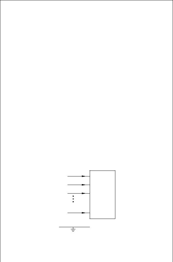
The derivation of this property is based on considering the currents in the indefinite circuit of Fig. 4.21. Jk is the current going into terminal k when all other terminals are connected to ground. It is therefore a result of independent current sources inside the n-port or currents resulting from initial conditions. The resulting currents going into each terminal are
i1 |
|
y11 |
y12 |
. . . y1n |
v1 |
|
J1 |
|
|
|
i.2 |
y.21 |
y.22 |
. . . |
y2.n |
v.2 |
J.2 |
4.143 |
|||
.. |
D |
.. |
.. |
... .. |
.. |
C |
.. |
|
|
|
in |
|
yn1 |
yn2 |
. . . |
ynn |
vn |
|
Jn |
|
|
|
|
|
|
|
|
|
|
|
|
|
The sum of all the equations represented by (4.143) gives the total current going into a node which by Kirchhoff’s law must be zero:
n n |
n |
n |
|
|
|
|
|
yjivi D |
ik |
Jk D 0 |
4.144 |
iD1 jD1 |
kD1 |
kD1 |
|
All the terminal voltages except the jth are set to 0 by connecting them to the external ground. Then, since vk D6 0, the only nonzero left-hand side of Eq. (4.144) would be
n |
|
|
|
vk yjk D 0. |
4.145 |
jD1 |
|
Thus the sum of the columns of the indefinite admittance matrix is 0.
V1 i 1
V2 i 2
V3 i 3
i n
Vn
FIGURE 4.21 An n-port indefinite circuit.

80 MULTIPORT CIRCUIT PARAMETERS AND TRANSMISSION LINES
The sum of the rows can also be shown to be 0. If the same voltage v0 is added to each of the terminal voltages, the terminal currents would remain unchanged:
i1 |
|
y11 |
y12 |
. . . y1n |
v1 C v0 |
|
J1 |
|
|
|||
i.2 |
y.21 |
y.22 |
. . . |
y2.n |
v2 C. v0 |
J.2 |
4.146 |
|||||
.. |
D |
.. |
.. |
... .. |
.. |
v0 |
C |
.. |
|
|
||
in |
|
yn1 |
yn2 |
. . . |
ynn |
vn |
|
|
Jn |
|
|
|
|
|
|
|
|
|
|
C |
|
|
|
|
|
Comparison of this with Eq. (4.143) shows |
|
|
|
|
||
y11 |
y12 |
. . . y1n |
v0 |
|
|
|
y.21 |
y.22 |
. . . y2.n |
v.0 |
0 |
4.147 |
|
.. |
.. ... .. |
.. |
D |
|
|
|
yn1 yn2 . . . ynn |
v0 |
|
|
|
||
|
|
|
|
|
|
|
So that the sum of the rows is 0. A variety of other important properties of the indefinite admittance matrix are described in [1, ch. 2] to which reference should be made for further details.
One of the useful properties of this concept is illustrated by the problem of converting common source hybrid parameters of a FET to common gate hybrid parameters. This might be useful in designing a common gate oscillator with a transistor characterized as a common source device. The first step in the process is to convert the hybrid parameters to the equivalent definite admittance matrix (which contains two rows and two columns) by using the formulas in Appendix E. The definite admittance matrix, which has a defined ground, can be changed to the corresponding 3 ð 3 indefinite admittance matrix by adding a column and a
row such that rows D 0 and the columns D 0. If the y11 corresponds to the gate and y22 corresponds to the drain, then y33 would correspond to the source:
g d |
s |
|
|
gy11 y12 y13
[Y] D d y21 |
y22 y23 |
4.148 |
sy31 y32 y33
The common gate parameters are found by forcing the gate voltage to be 0. Consequently the second column may be removed, since it is multiplied by the zero gate voltage anyway. At this point the second row represents a redundant equation and can be removed. In this case row 2 and column 2 are deleted, and a new common gate definite admittance matrix is formed. This matrix can then be converted to the equivalent common gate hybrid matrix.
4.10THE INDEFINITE SCATTERING MATRIX
A similar property can be determined for the scattering matrix. The indefinite scattering matrix has the property that the sum of the rows D 1 and the sum