

03.Impedance matching
.pdfTAPPED CAPACITOR TRANSFORMER |
43 |
R s
C p |
R p |
= |
C s
FIGURE 3.9 Parallel RC to series RC conversion.
course valid for only a narrow frequency range, so this method is fundamentally limited by this approximation.
The impedance of the parallel circuit is
Rp |
3.35 |
Zp D 1 C sCpRp |
The Q for a parallel circuit is Qp D ωCpRp. The equivalent series resistance and reactance in terms of Qp are
Rseqv D |
|
Rp |
|
3.36 |
1 C Qp2 |
||||
Xseqv D |
XpQp2 |
3.37 |
||
1 C Qp2 |
||||
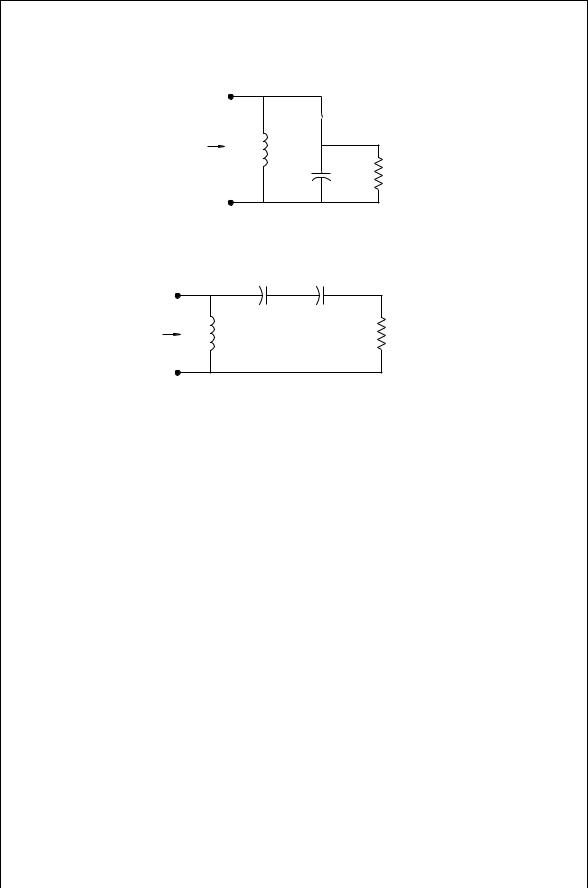
3.8.2Conversion of Tapped C Circuit to an L-Shaped Circuit
The schematic of the tapped C circuit is shown in Fig. 3.10 where R0 is to be matched to R2. The parallel R2C2 section is converted to a series ReqvCeqv, as indicated in Fig. 3.11. Making use of Eqs. (3.36) and (3.37),
Cseqv D C2 |
|
1 C Qp2 |
for high Qp |
||
|
|
|
³ C2 |
||
|
Qp2 |
||||
Rseqv D R D |
|
R2 |
|
|
|
1 C Qp2 |
|
|
|||
where Qp D ω0C2R2. Considering R0 as the load, and using the L formation for a shunt circuit in Table 3.1,
R0
Rseqv D 1 C Q12
3.38
3.39
circuit trans-
3.40
44 IMPEDANCE MATCHING
 C 1
C 1
R ' |
L |
C 2 |
R 2 |
FIGURE 3.10 Tapped C transformation circuit.
|
C1 |
C seq v |
R ' |
L |
R = R seq v |
FIGURE 3.11 Intermediate equivalent transformation circuit.
This is the transformed resistance looking through C1 toward the left. Looking toward the right through Cseqv and again using the parallel to series conversion, Eq. (3.36),
|
Rseqv D |
R2 |
|
|
3.41 |
||
|
1 C Qp2 |
|
|||||
These two expressions for Rseqv can be equated and solved for Qp: |
|
||||||
Qp D |
R 1 C Q12 1 |
1/2 |
3.42 |
||||
|
|||||||
|
|
R2 |
|
|
|
|
|
3.8.3Calculation of Circuit Q
An approximate value for Q can be found by equating the impedances of the two circuits in Fig. 3.12:
Z |
D |
R0ω2L2 C jR02ωL |
D |
R0 |
C |
jωL |
eqv |
3.43 |
|
R02 C ωL 2 |
|||||||||
|
eqv |
|
|
If the Q of the right-hand circuit is approximately that of the left-hand circuit in Fig. 3.12, then
Q1 D |
ω0Leqv |
D |
ω0R02L |
D |
R0 |
3.44 |
Reqv0 |
R0ω02L2 |
ω0L |
|
|
|
PARALLEL DOUBLE-TUNED TRANSFORMER |
45 |
||
|
|
C |
|
L eq v |
C |
|
R ' |
L |
Z |
Q 1 |
R 'eq v |
Z |
|
FIGURE 3.12 Equate the leftand right-hand circuits.
TABLE 3.4 Tapped C Matching Circuit Design Formulas
Step Number |
|
|
|
|
Tapped C Formula |
|
|||||||
|
|
|
|
|
|
|
|||||||
1 |
Q1 D f0/ f |
|
|
|
|
|
|||||||
2 |
C |
D |
Q /ω |
R0 |
|
D |
1/2 fR0 |
||||||
|
|
|
1 |
2 |
0 |
|
|
|
|
|
|||
3 |
L D 1/ω0C |
0 2 |
2 |
2 |
1/2 |
||||||||
5 |
C2 |
D |
p |
|
|
|
|||||||
4 |
Qp |
D |
R2 |
/R0 |
1 C Q12 |
1 |
|
||||||
|
|
|
|
|
Q /ω R |
|
|
|
|
||||
6 |
Cseqv D C2 1 C Qp /Qp |
|
|||||||||||
7 |
C1 |
D CseqvC2/ Cseqv C2 |
|
||||||||||
The variable C represents the total capacitance of C1 and Cseqv in series, as implied in Fig. 3.11 and represented in Fig. 3.12. For a high Q circuit, circuit analysis gives the resonant frequency:
ω02 |
1 |
|
|
|
1 |
|
3.45 |
|
D |
|
³ |
|
|
|
|||
LC L2/R02 |
LC |
|||||||
As a result the approximate value for Q1 can be found: |
|
|||||||
|
Q1 D ω0R0C D |
f0 |
|
|
3.46 |
|||
|
f |
|
|
|||||
Here f is the bandwidth in Hz and f0 is the resonant frequency.
3.8.4Tapped C Design Procedure
The above ideas are summarized in Table 3.4, which provides a design procedure for the tapped C matching circuit. Similar expressions could be found for a tapped inductor transforming circuit, but such a circuit is typically less useful because inductors are more difficult to obtain than capacitors.
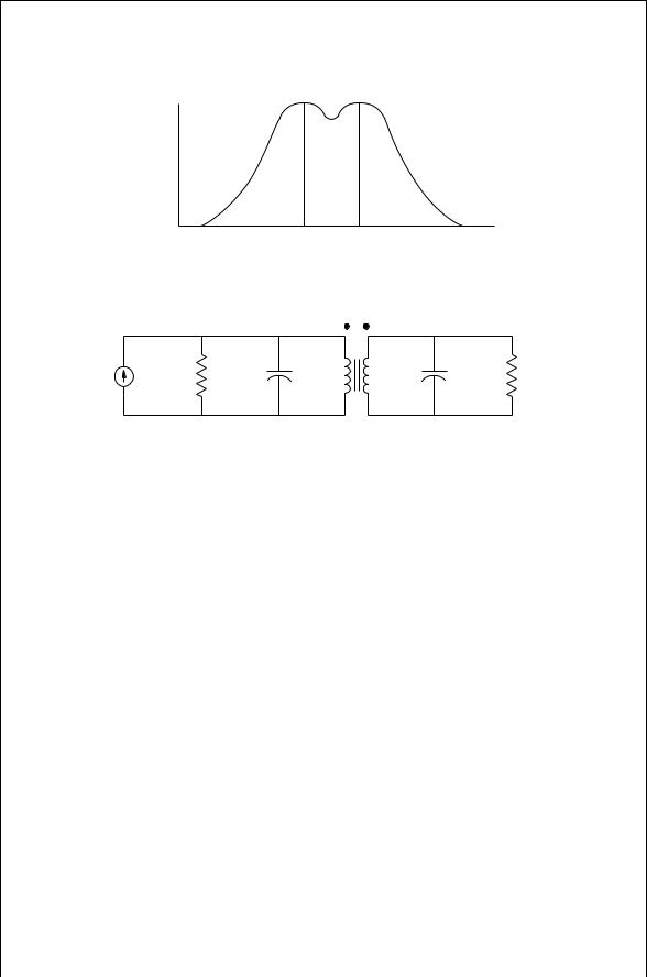
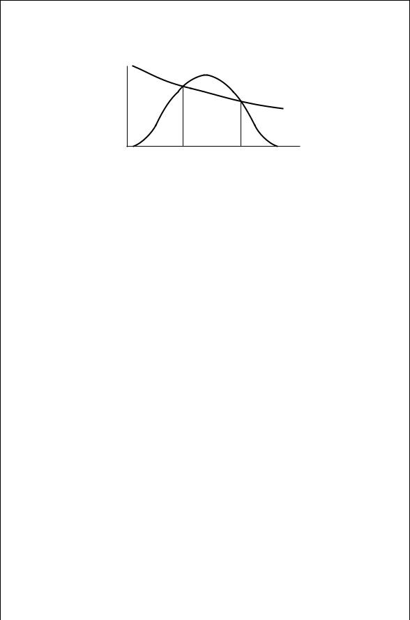
3.9PARALLEL DOUBLE-TUNED TRANSFORMER
Each of the above described T, , or tapped C matching circuits provide some control over the bandwidth. Where precise control over the bandwidth is required, a double tuned circuit allows controlling bandwidth by specifying two different frequencies where maximum transmission occurs. For a small pass band, the
46 IMPEDANCE MATCHING
G T
f m1 f m2
FIGURE 3.13 Double tuned transformer response.
M
R G |
C1 |
L11 |
L 22 |
C 2 |
RL |
FIGURE 3.14 Real transformer with resonating capacitances.
midband dip in the transmission can be made small. Furthermore the double-tuned circuit is especially useful when a large difference in impedance levels is desired although its high end frequency range is limited. The filter transmission gain is shown in Fig. 3.13.
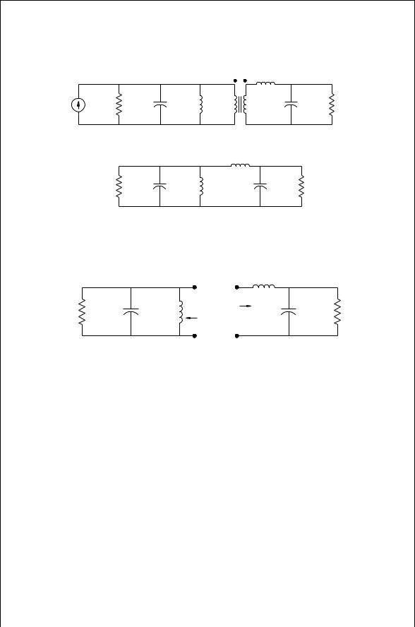
The double-tuned circuit consists of a coupled coil transformer with resonating capacitances on the primary and secondary side. This circuit is shown in Fig. 3.14. The transformer is described by its input and output inductance as well as the coupling coefficient k. The turns ratio for the transformer is
n : 1 D |
|
|
k2L22 |
: 1 |
3.47 |
|
|
|
L11 |
|
|
The circuit in Fig. 3.14 can be replaced by an equivalent circuit using an ideal transformer (Fig. 3.15a). Since an ideal transformer has no inductance, the inductances and coupling factor, k, must be added to the ideal transformer. The final circuit topology is shown in Fig. 3.15b. Looking toward the right through the ideal transformer, Fig. 3.15b shows the circuit values are:
L20 |
D L11 |
1 |
1 |
3.48 |
|||
k2 |
|||||||
C20 |
D k2L22 C2 |
3.49 |
|||||
|
|
|
L11 |
|
|||
RL0 |
|
L11 |
3.50 |
||||
D |
|
RL |
|||||
k2L22 |
|||||||
|
|
PARALLEL DOUBLE-TUNED TRANSFORMER |
47 |
||
|
|
n :1 |
L 22(1–k 2) |
|
|
R G |
C 1 |
L11 |
C 2 |
R L |
|
(a )
L '2
R G |
C 1 |
L 11 |
C '2 |
R 'L |
(b )
FIGURE 3.15 (a) Alternate equivalent circuit with an ideal transformer, and (b) final equivalent circuit.
|
|
|
|
L '2 |
|
|
R G |
C 1 |
L 11 |
R 2 |
C '2 |
R 'L |
|
R 1 |
||||||
|
|
|
|
|
FIGURE 3.16 Double tuned circuit split into two.
The circuit elements will be chosen to give exact match at the two frequencies, fm1 and fm2. The circuit in Fig. 3.15b can be conceptually split into two (Fig. 3.16). The resistance R1 with the parallel resonant circuit will never be larger than RG. The right-hand side is an L matching circuit with the reactance of the shunt element monotonically decreasing with frequency. Hence R2 monotonically decreases. Consequently, if RL is small enough, there will be two frequencies where R1 D R2. This is illustrated in Fig. 3.17.
A design procedure for the parallel double-tuned circuit has been reviewed in [1] and is summarized below. The typical synthesis problem is to design a circuit that will match RG and RL over a bandwidth, f, at a center frequency, f0, with a given pass band ripple. The bandwidth and center frequency are approximated by the following:
1. Determine fm1 and fm2:
p |
|
|
|
|
|
f ³ 2 fm2 fm1 |
3.51 |
||||
f0 ³ |
fm1fm2 |
|
3.52 |
||
48 IMPEDANCE MATCHING
Resistance
f m1 |
f m2 |
R 2
R 1
FIGURE 3.17 Plot of leftand right-hand resistance values versus frequency.
The minimum pass band gain for the filter is dependent on the difference between the match frequencies:
GTmin D |
4fm2/fm1 |
3.53 |
|
fm2/fm1 2 C 2fm2/fm1 C 1 |
|
||
2. Determine the actual transducer gain for the given ripple factor: |
|
||
GT D 10 ripple factor dB /10 |
3.54 |
||
3.Find the resistance ratio if GT > GTmin, the pass band ripple specification can be met:
|
|
r |
D |
1 C j1 GTj1/2 |
|
|
|
||||||||
|
|
|
1 j1 GTj1/2 |
|
|
|
|
||||||||
4. |
Calculate the Q2 at the two matching frequencies: |
|
|
||||||||||||
|
|
Q22 m1 D r |
fm1 |
|
1 |
|
|
|
|
||||||
|
|
fm2 |
|
|
|
|
|||||||||
|
|
Q22 m2 D r |
fm2 |
|
1 |
|
|
|
|
||||||
|
|
fm1 |
|
|
|
|
|||||||||
5. |
Solve the following simultaneous equations for L20 |
and C20 : |
|||||||||||||
|
ωm1L20 |
C |
1 |
|
D jQ2 m1j |
|
|
|
RG |
||||||
|
|
|
|
|
|
|
|
||||||||
|
ω |
C0 |
1 |
C |
Q2 |
|
|||||||||
|
|
|
m1 |
2 |
|
|
|
|
|
|
2 m1 |
||||
|
Cωm2L20 |
C |
1 |
|
D jQ2 m2j |
|
|
|
RG |
||||||
|
ωm2C20 |
1 C Q22 m2 |
|
||||||||||||
6. |
Find the value for RL0 : |
|
|
|
|
1 C Q22 m1 |
|
|
|
|
|
|
|||
|
|
|
R0 |
D |
|
|
|
|
|
|
|||||
|
|
|
L |
ωm2 1C202RG |
|
|
|
|
|
|
|||||
3.55
3.56
3.57
3.58
3.59
3.60

PARALLEL DOUBLE-TUNED TRANSFORMER |
49 |
7. Calculate the input susceptance of the right-hand side where G0L D 1/RL0 :
Bm1 D Im jωm1L20 |
C 1/GL0 |
C jωm1C20 |
|
||
|
|
1 |
|
|
|
Bm2 D Im jωm2L20 |
C 1/GL0 |
C jωm2C20 |
|
||
|
|
1 |
|
|
|
8. Solve the following simultaneous equations for L11 and C1:
1
ωm1C1 D jBm1j
ωm1L11
1
ωm2C1 D jBm2j
ωm2L11
9. Find the transformer coupling coefficient, and hence L22 and C2:
1
k D
1 C L20 /L11
L11RL
L22 D k2RL0
C2 D L11 C02
k2L22
3.61
3.62
3.63
3.64
3.65
3.66
3.67
This procedure has been coded into the program DBLTUNE, and an example of its use is given in Appendix C.
PROBLEMS
3.1Design an impedance transforming network that matches a generator resistance, RG D 400 " to a load resistance RL D 20 ". The center frequency for the circuit is f0 D 6 MHz. The desired ripple (where appropriate) is to be less than 0.25 dB. In some cases the ripple factor will not be able to be controlled in the design. The problem is to design four different transformation circuits with the specifications above, and for each design do an analysis using SPICE. See Appendix G, Sections G.1, and G.2.
(a)Design a two-element L matching circuit and check the results with SPICE.
(b)Design a three-element tapped capacitor matching circuit with a bandwidth f D 50 kHz, and check the results with SPICE to determine the actual bandwidth.

50IMPEDANCE MATCHING
(c)Design a three-element matching circuit with a bandwidth of f D 50 kHz, and check the results with SPICE to determine the actual bandwidth.
(d)Design a double tuned transformer matching circuit with a bandwidth off D 50 kHz, and check the results with SPICE to determine the actual bandwidth.
(e)Repeat part (d) for a 3 dB bandwidth of 2 MHz. Again, check the results using SPICE.
3.2The matching circuit shown in Fig. 3.4 is used to match the load R D 1000 " to R00 D 80 ". If the intermediate resistance level is R0 D 20 ", determine the following:
(a)What is Q1?
(b)What is Q2?
(c)What is B1, the first susceptance nearest R?
(d)What is the estimated 3 dB bandwidth for this circuit in terms of the center frequency, f0?
3.3The tapped capacitor transformer is to be used in a narrowband of frequencies around ω D 4 Ð 109 rad/s. In designing the matching circuit, the tapped C circuit is converted to an ‘L’ matching circuit. If R2 in Fig. 3.10 is 50 ", C2 D 8 pF, and C1 D 5.0 pF, then what is the total capacitance for the ‘L’ matching circuit?
REFERENCES
1.P. L. D. Abrie, The Design of Impedance-Matching Networks for Radio-Frequency and Microwave Amplifiers, Norwood, MA: Artech House, 1985.