

01_elektor_electronics_UK_january_2006
.pdfELECTRICAL SAFETY INFO & MARKET
In all mains-operated equipment certain important safety requirements must be met. The relevant standard for most sound equipment is Safety of Information Technology Equipment, including Electrical Business Equipment (European Harmonized British Standard BS EN 60950:1992). Electrical safety under this standard relates to protection from
•a hazardous voltage, that is, a voltage greater than 42.4 V peak or 60 V d.c.;
•a hazardous energy level, which is defined as a stored energy level of 20 Joules or more or an available continuous power level of 240 VA or more at a potential of 2 V or more;
•a single insulation fault which would cause a conductive part to become hazardous;
•the source of a hazardous voltage or energy level from primary power;
•secondary power (derived from internal circuitry which is supplied and isolated from any power source, including d.c.)
Protection against electric shock is achieved by two classes of equipment.
Class I equipment uses basic insulation ; its conductive parts, which may become hazardous if this insulation fails, must be connected to the supply protective earth.
Class II equipment uses double or reinforced insulation for use where there is no provision for supply protective earth (rare in electronics – mainly applicable to power tools).
The use of a a Class II insulated transformer is preferred, but note that when this is fitted in a Class I equipment, this does not, by itself, confer Class II status on the equipment.
Electrically conductive enclosures that are used to isolate and protect a hazardous supply voltage or energy level from user access must be protectively earthed regardless of whether the mains transformer is Class I or Class II.
Always keep the distance between mains-carrying parts and other parts as large as possible, but never less than required.
If at all possible, use an approved mains entry with integrated fuse holder and on/off switch. If this is not available, use a strain relief (Figure, note 2) on the mains cable at the point of entry. In this case, the mains fuse should be placed after the double-pole on/off switch unless it is a Touchproof® type or similar. Close to each and every fuse must be affixed a label stating the fuse rating and type.
The separate on/off switch (Figure, note 4), which is really a ‘disconnect device’, should be an approved doublepole type (to switch the phase and neutral conductors of a single-phase mains supply). In case of a three-phase supply, all phases and neutral (where used) must be switched simultaneously. A pluggable mains cable may be considered as a disconnect device. In an
approved switch, the contact gap in the off position is not smaller than 3 mm.
The on/off switch must be fitted by as shor t a cable as possible to the mains entry point. All components in the primary transformer circuit, including a separate mains fuse and separate mains filtering components, must be placed in the switched section of the primary circuit. Placing them before the on/off switch will leave them at a hazardous voltage level when the equipment is switched off.
If the equipment uses an open-con- struction power supply which is not separately protected by an ear thed metal screen or insulated enclosure or otherwise guarded, all the conductive parts of the enclosure must be protectively earthed using green/yellow wire (green with a narrow yellow stripe – do not use yellow wire with a green stripe). The ear th wire must not be daisychained from one part of the enclosure to another. Each conductive part must be protectively earthed by direct and separate wiring to the primary ear th point which should be as close as possible to the mains connector or mains cable entry. This ensures that removal of the protective earth from a conductive part does not also remove the protective ear th from other conductive parts.
Pay particular attention to the metal spindles of switches and potentiometers: if touchable, these must be protectively earthed. Note, however, that such components fitted with metal spindles and/or levers constructed to the relevant British Standard fully meet all insulation requirements.
The temperature of touchable parts must not be so high as to cause injury or to create a fire risk.
Most risks can be eliminated by the use of correct fuses, a sufficiently firm construction, correct choice and use of insulating materials and adequate cooling through heat sinks and by extractor fans.
The equipment must be sturdy: repeatedly dropping it on to a hard surface from a height of 50 mm must not cause damage. Greater impacts must not loosen the mains transformer, electrolytic capacitors and other important components.
Do not use dubious or flammable materials that emit poisonous gases.
Shor ten screws that come too close to other components.
Keep mains-carrying par ts and wires well away from ventilation holes, so that an intruding screwdriver or inward falling metal object cannot touch such parts.
As soon as you open an equipment, there are many potential dangers. Most of these can be eliminated by disconnecting the equipment from the mains before the unit is opened. But, since testing requires that it is plugged in again, it is good practice (and safe) to fit a residual current device (RCD)*, rated at not more than 30 mA to the
1.Use a mains cable with moulded-on plug.
2.Use a strain relief on the mains cable.
3.Affix a label at the outside of the enclosure near the mains entry stating the equipment type, the mains voltage or voltage range, the frequency or frequency range, and the current drain or curent drain range.
4.Use an approved double-pole on/off switch, which is effectively the ‘disconnect device’.
5.Push wires through eyelets before soldering them in place.
6.Use insulating sleeves for extra protection.
7.The distance between transformer terminals and core and other parts must be ≥ 6 mm.
8.Use the correct type, size and current-carrying capacity of cables and wires
– see shaded table below.
9.A printed-circuit board like all other parts should be well secured. All joints and connections should be well made and soldered neatly so that they are mechanically and electrically sound. Never solder mains-carrying wires directly to the board: use solder tags. The use of crimp-on tags is also good practice.
10.Even when a Class II transformer is used, it remains the on/off switch whose function it is to isolate a hazardous voltage (i.e., mains input) from the primary circuit in the equipment. The primary-to-secondary isolation of the transformer does not and can not perform this function.
mains system (sometimes it is possible to fit this inside the mains outlet box or multiple socket).
* Sometimes called residual current breaker – RCB – or residual circuit current breaker –RCCB.
These guidelines have been drawn up with great care by the editorial staff of
this magazine. However, the publishers do not assume, and hereby disclaim, any liability for any loss or damage, direct or consequential, caused by errors or omissions in these guidelines, whether such errors or omissions result from negligence, accident or any other cause.
3-core mains cable to BS6500 1990 with three stranded conductors in thick PVC sheath
Max current |
3 A |
6 A |
13 A |
conductor size |
16/0.2 mm |
24/0.2 mm |
40/0.2 mm |
Nom cond area |
0.5 mm2 |
0.75 mm2 |
1.25 mm2 |
overall cable dia. |
5.6 mm |
6.9 mm |
7.5 mm |
Insulated hook-up wire to DEF61-12 |
|
|
|
Max current |
1.4 A |
3 A |
6 A |
Max working voltage |
1000 V rms |
1000 V rms |
1000 V rms |
PVC sheath thickness |
0.3 mm |
0.3 mm |
0.45 mm |
conductor size |
7/0.2 mm |
16/0.2 mm |
24/0.2 mm |
Nom cond area |
0.22 mm2 |
0.5 mm2 |
0.95 mm2 |
overall wire dia |
1.2 mm |
1.6 mm |
2.05 mm |
3-flat-pin mains plug to BS 1363A
1/2006 - elektor electronics |
61 |

HANDS-ON MODDING
A ‘Retro’ Mobile
Give an old phone a second life
Thijs Beckers
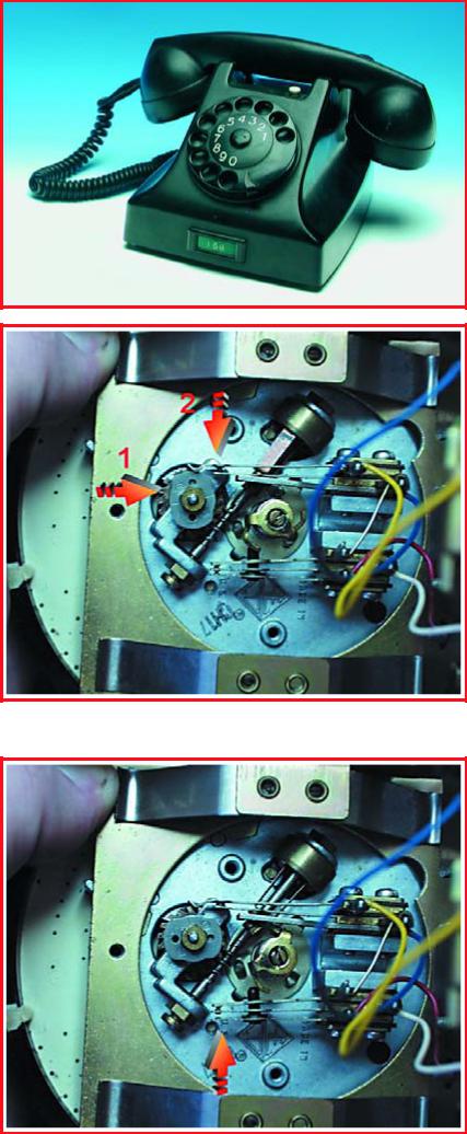
Old-fashioned bakelite telephones are becoming increasingly rare in living rooms, but they’re still common enough at rummage sales. We like convenience in our lives and our tools, and a phone that isn’t attached to the wall by a cord is simply more convenient. So it’s ‘out with the old, in with the new’ where phones are concerned.
62 |
elektor electronics - 1/2006 |
Phone
Stop! Don’t throw away your old phone! You can give it a second life using the circuit described in this article. That makes a nice Christmas present (maybe a bit belated) or gimmick, although it’s naturally a bit too heavy to carry around wherever you go. However, it’s perfect on your desk at work or in the pub. You’re bound to draw a second glance or be accused of being off your head, but that will change when the phone rings – despite not having the usual cable – and you start having a lively conversation.
What’s inside
Old phones are primarily based on mechanical systems, because there weren’t any PICs or microcontrollers fifty years ago. The mechanism behind the dial is no longer used, but that doesn’t mean it wasn’t a well-consid- ered design, far from it.
Figure 1 shows how it works. When you dial a digit, the small, grey oval wheel (arrow 1) rotates once for every two digit positions while the dial is returning to its starting point. As a result, the contacts (arrow 2) generate a pulse for each digit position on the dial. The microcontroller uses these pulses to determine which number you dial.
Figure 2 shows the mechanism with the dial in the rest state. The other set of contacts (marked by the arrow) is open in this state. That tells the microcontroller that the dial has stopped rotating.
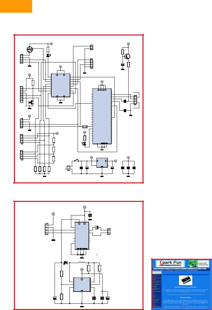
We use a 16LF88 microcontroller here. Figure 3 shows how it is connected to the rest of the circuit. The firmware can be downloaded free of charge from our website.
A 3.7-V lithium polymer battery provides the supply voltage. Although the minimum supply voltage is specified as 4 V in the 16LF88 data sheet, it still
1/2006 - elektor electronics
Figure 1. Good news: the mechanical construction of a 50-year-old phone is compatible with modern microcontrollers. The small grey wheel generates a series of pulses after you turn and release the dial.
Figure 2. The lower set of contacts (see arrow) provides an electrical indication that the dial is at rest.
63
HANDS-ON MODDING
|
|
|
|
|
|
+3V8 |
|
|
|
|
|
|
|
|
|
|
|
|
|
|
+3V3 |
|
|
|
|
|
|
|
|
|
|
|
|
|
|
K5 |
|
|
|
|
|
|
|
|
|
|
|
|
T1 |
S |
|
|
|
R2 |
|
|
|
|
|
|
|
|
|
|
|
|
|
|
|
|
|
|
|
|
G |
|
|
|
|
|
|
|
|
|
|
|
|
|
|
|
|
|
|
|
|
|
|
|
|
|
Ω |
|
|
|
|
|
|
|
|
|
|
|
|
|
|
R12 |
|
|
|
|
|
|
|
|
|
|
|
|
|
|
|
|
|
|
|
|
|
|
|
|
|
||
|
|
|
|
|
|
330 |
|
|
|
|
|
|
|
|
|
|
|
|
|
|
|
|
|
|
K4 |
|
|
|
|
|
|
|
|
|
hook contact |
|
|
|
|
|
|
10k |
|
|
|||
|
|
|
|
|
|
|
|
|
|
|
|
|
|
|
|
|
|
|
T2 |
|
|||
|
D |
IRF7220 |
|
|
D1 |
|
|
|
|
|
|
|
|
|
|
|
|
|
|
|
|
||
|
|
|
|
|
|
PIC STATUS |
|
|
|
|
K3 |
|
|
|
|
|
|
|
|
|
|
|
|
|
|
|
|
|
|
|
|
|
|
|
|
|
|
|
|
|
|
|
|
|
|
||
|
|
|
|
|
|
|
|
|
|
|
|
|
rotary dial (number) |
|
|
R4 |
|
||||||
|
|
|
|
|
|
|
|
|
|
|
|
|
|
|
|
|
|
|
|
|
C3 |
|
|
|
|
|
|
|
|
|
|
|
|
|
|
|
|
|
|
|
|
|
|
|
2k2 |
|
|
|
ringer |
|
|
|
|
|
+3V8 |
|
|
|
|
rotary dial (rest contact) |
|
10 |
|
||||||||
|
circuit |
|
|
|
|
|
|
|
|
|
|
|
|
|
|
|
|
|
|
|
|
|
|
|
+3V8 |
|
|
|
15 |
|
16 |
|
|
|
|
|
|
|
|
|
|
|
|
|
|
||
|
|
|
|
|
|
19 |
RA0/AN0 |
|
RB0 |
7 |
|
|
|
|
|
|
|
|
|
|
|
|
|
|
|
|
R3 |
|
|
20 |
RA1/AN1 |
IC1 |
RB1 |
8 |
|
|
|
|
+3V8 |
|
|
|
|
|
|
|
|
|
|
|
10k |
|
|
1 |
RA2/VREF- |
RB2/RX |
9 |
|
|
|
|
|
|
|
|
|
|
|
|
|
|
|
|
|
|
|
|
|
|
|
|
|
|
|
|
|
|
|
|
|
|||||
|
|
|
|
|
2 |
|
10 |
|
|
|
|
|
|
|
|
|
|
|
|
|
|||
|
CON2 |
|
|
|
RA3/VREF+ |
|
RB3 |
|
|
|
|
|
|
|
|
|
|
|
|
|
|||
|
|
|
|
|
|
|
|
|
|
|
|
|
|
|
|
|
|
|
|
|
|||
|
|
|
|
|
3 |
RA4/AN4 16LF88 |
RB4 |
11 |
|
|
|
|
|
|
|
|
|
|
|
|
|
||
interface |
|
|
|
|
|
|
|
|
|
|
|
|
|
|
|
|
|
|
|||||
|
|
|
|
|
4 |
-SSOP |
RB5/TX |
12 |
|
|
|
1 |
3 |
5 |
7 |
|
|
|
|
|
|||
|
|
|
|
|
17 |
RA5/VPP |
|
13 |
|
|
|
|
|
|
|
|
|
|
|
|
|
||
|
|
|
|
|
RA6/OSC2 |
RB6/AN5/PGC |
|
|
|
|
|
|
CHARGE |
8 |
|
loudspeaker |
|||||||
|
|
|
|
|
18 |
RA7/OSC1 |
RB7/AN6/PGD |
14 |
|
9 |
|
|
|
|
10 |
|
|
|
|||||
programming |
|
|
|
|
|
|
|
|
EAR_HF+ |
|
|
EAR_MT- |
|
|
K2 |
||||||||
|
|
|
|
|
|
|
|
|
|
|
11 |
EAR_HF- |
|
|
EAR_MT+ |
12 |
|
|
|
||||
S2 |
|
|
|
|
5 |
|
6 |
|
|
13 |
MIC_HF- |
|
|
MIC_MT+ |
14 |
C1 |
|
|
|||||
|
|
|
|
|
|
|
|
|
15 |
MIC_HF+ |
|
|
MIC_MT- |
16 |
|
|
|
||||||
|
|
|
|
|
|
|
|
|
|
|
17 |
ON/OFF |
|
|
|
|
AXE |
18 |
100n |
|
|||
|
|
|
|
|
|
|
|
|
|
|
|
|
|
|
|
|
|||||||
|
|
|
RESET |
|
|
|
|
|
|
|
|
19 |
SIMIO |
MOD1 |
|
|
TX |
20 |
|
|
|
||
|
|
|
|
|
|
|
|
|
|
|
21 |
PWRCTL |
|
|
SIMVCC |
22 |
C9 |
|
microphone |
||||
|
|
|
|
|
|
|
|
|
|
|
|
23 |
RST |
|
|
|
SIMRST |
24 |
|
|
|||
|
|
|
|
|
|
|
|
|
|
|
|
|
|
|
|
|
|
||||||
|
+3V8 |
|
|
|
|
|
|
|
|
25 |
MONI_CAM |
|
SIMCLK |
26 |
220n |
|
|
||||||
|
|
|
|
|
|
|
|
|
27 |
CCIN |
|
|
|
|
GPIO2 |
28 |
|
|
|
||||
|
CON1 |
|
|
|
|
|
|
|
|
|
|
29 |
CTS |
|
|
|
|
|
RI |
30 |
|
|
|
|
|
|
|
|
|
|
|
|
|
|
|
31 |
GPIO1 |
|
|
|
|
PD0 |
32 |
|
|
|
|
|
TX |
|
|
|
|
|
|
|
|
TX |
|
33 |
DSR |
|
|
|
|
|
PD1 |
34 |
|
|
|
|
|
|
|
|
|
|
|
|
JP1 |
35 |
EMMI_TX |
|
|
|
|
DCD |
36 |
|
|
|
|||
|
RX |
|
|
|
|
|
|
|
|
RX |
|
37 |
RX |
GM862 |
|
PD2 |
38 |
|
|
|
|||
|
debug |
|
|
|
|
|
|
|
|
|
+3V8 |
39 |
STATUS |
|
|
|
|
PD3 |
40 |
|
|
|
|
|
|
|
|
|
|
|
+3V8 |
|
|
|
41 |
EMMI_RX |
|
|
|
|
PD4 |
42 |
|
|
|
||
|
K6 |
|
|
|
|
|
|
|
|
|
R1 |
43 |
DTR |
|
|
|
|
|
PD5 |
44 |
|
|
|
|
|
|
|
|
|
|
|
|
|
|
45 |
RTS |
|
|
|
|
GPIO3 |
46 |
|
|
|
||
|
|
|
|
|
|
|
R9 |
|
|
|
Ω |
47 |
|
|
|
|
|
|
|
48 |
|
|
|
|
|
|
|
|
|
|
|
|
|
330 |
GPIO4 |
|
|
|
GPIO5 |
|
|
|
|||||
|
|
|
|
|
|
|
4k7 |
|
|
|
49 |
GPIO6 |
|
|
|
GPIO7 |
50 |
|
|
|
|||
|
|
|
|
|
|
|
|
|
|
|
D2 |
|
|
|
|
|
|
|
|
|
|
|
|
|
number pad 1 |
|
|
|
|
|
R10 |
|
|
|
|
|
|
|
2 |
|
4 |
|
6 |
|
|
|
|
|
|
|
|
|
|
|
|
|
|
|
|
|
|
|
|
|
|
|
|
|
|
|
|
|
K7 |
|
|
|
|
|
10k |
|
|
|
GM862 STATUS |
|
|
|
|
|
|
|
|
|
|
|
|
|
|
|
|
|
|
|
|
|
|
|
|
|
|
|
|
|
|
|
|
|
|
||
|
|
|
|
|
|
|
R11 |
|
|
|
|
+3V8 |
|
IC2 |
|
|
|
|
|
|
+3V8 |
|
|
|
|
|
|
|
|
|
10k |
|
|
|
S1 |
|
|
TPS73133 |
|
|
+3V3 |
|
|
|
|||
|
|
|
|
|
|
|
|
|
|
|
1 |
V-REG |
|
|
5 |
|
|
|
|||||
|
number pad 2 |
|
|
|
|
|
|
|
|
|
|
|
|
|
|
|
|
|
|||||
|
|
|
|
|
|
|
|
|
|
|
|
|
|
|
|
|
|
|
|
||||
|
|
|
|
|
|
|
|
|
|
POWER |
|
|
|
LDO |
|
|
|
|
|
|
|
|
|
|
|
|
|
|
|
|
|
|
K1 |
|
|
|
|
|
|
|
|
|
|
|
|
||
|
|
|
R8 |
R7 |
R6 |
R5 |
|
|
|
|
|
3 |
EN 150mA NC |
4 |
|
|
|
|
|||||
|
|
|
|
+3V7 |
|
|
C2 |
C4 |
C8 |
C5 |
C6 |
C7 |
|||||||||||
|
|
|
10k |
10k |
10k |
10k |
|
|
|
|
|
|
|
|
|
|
|
|
|
|
|
|
|
|
|
|
|
LiPoly |
|
100p |
100 |
|
|
2 |
|
|
|
|
10 |
100n |
100n |
100n |
|||||
|
|
|
|
|
|
|
|
|
|
|
|
|
|
|
|
|
|
||||||
|
|
|
|
|
|
|
|
|
|
|
|
|
|
|
|
|
|
|
|
050317 - 11 |
|
|
|
Figure 3. The schematic diagram of the control unit for the circuit. Most of the circuitry is contained in the GM82 and 16LF88, so only a few external components are necessary.
|
|
|
|
+U |
|
|
|
|
|
+U |
|
|
|
|
|
C1 |
|
|
|
|
|
|
|
|
|
|
|
|
|
|
|
|
|
|
|
100n |
|
|
|
K1 |
|
|
8 |
16 |
|
|
|
|
|
|
|
2 |
|
1 |
|
3C23* |
|
|
|
|
1 |
|
|
|
|
K2 |
|||
|
1,2EN |
|
|
|
|
|
|||
|
2 |
1A |
IC1 |
1Y |
3 |
100V |
|
|
|
|
7 |
2A |
2Y |
6 |
|
|
|
||
to ringer |
10 |
SN754410 |
11 |
|
|
to ringer |
|||
circuit |
3A |
|
|
3Y |
|
|
|
||
|
15 |
4A |
|
|
4Y |
14 |
|
|
|
|
9 |
3,4EN |
|
|
|
|
|
|
|
|
|
4 |
5 |
12 |
13 |
|
|
|
|
|
D1 |
|
|
|
|
|
*see text |
|
|
|
|
|
|
|
|
|
|
|
|
|
1N5822 |
|
L1 |
|
|
|
|
|
|
|
|
|
|
|
|
|
|
|
|
|
|
|
150 H |
R4 |
R3 |
|
|
||
|
|
|
+U |
0Ω 25 |
|
180 Ω |
|
|
|
|
R1 |
|
|
|
|
|
|
||
|
47k |
IC2 |
|
|
|
|
|
|
|
|
|
|
6 |
|
|
|
|
|
|
|
1 |
SWI COL |
I SENS |
7 |
|
|
|
||
|
5 |
COMP IN |
DRI COL |
8 |
|
|
|
||
|
2 |
3 |
|
|
|
||||
|
SWI EMI |
TIM CAP |
|
|
|
||||
|
R2 |
|
|
4 |
|
|
|
|
|
C3 |
1k |
|
|
MC34063A |
C4 |
C5 |
C6 |
||
|
|
|
|
|
|||||
1000 63V |
1n |
100n 1000 |
10V
050317 - 12
works at 3.7 V (actually 3.8 V). The GSM module draws a peak current of around 2 A, which is more than most voltage regulator ICs like to provide, but a LiPo battery simply shrugs its shoulders.
The GM862 module comes from Spark Fun Electronics. It is a GSM module that can handle three bands: 900 MHz, 1800 MHz and 1900 MHz. The microphone and speaker of the telephone are connected to it via K2. The module can drive most types of speakers directly. The sensitivity of the microphone input is 50 mV, so you can probably manage without amplifying the microphone signal. A coupling capacitor and a resistor connected to the supply voltage to power the electret microphone should be sufficient. Connect the dial contacts to K3 and the ‘offhook’ contact to K5.
The GSM module can be controlled by the PIC using AT commands. CON1 and CON2 provide convenient debug access. K6 and K7 were added for connecting an optional keyboard, and they can be omitted.
The ringer circuit is energised via K4 (see Figure 4). It has the difficult task of converting a 3.8-V DC signal to an AC voltage at around 60 V. A boost converter followed by an H bridge is used for this purpose. The relatively high voltage is necessary to make the clappers strike the bells with sufficient force. The frequency of the AC voltage determines how fast the bell rings. The ringer coil and C2 form a resonant circuit with a frequency of approximately 22 Hz. Of course, the value of C2 can be adjusted to suit the electromagnetic ringer used in your phone.
If all of this is a bit too much work for you, you can visit the Spark Fun website to order a ready-made telephone.
(050317-1)
Figure 4. The schematic diagram of the boost converter. This circuit generates the relatively high voltage |
Web link: |
needed to drive the electromagnetic ringer. |
www.sparkfun.com |
64 |
elektor electronics - 1/2006 |

£ |
Ó |
x
{
Î
ÊV «iÀ>Ì ÊÜ Ì Ê >ÌÀ ÝÊ Õ Ì i` >]ÊÌ iÊ > Õv>VÌÕ ÀiÀÊ vÊ L V Ã]ÊÜiÊ>ÀiÊ>L iÊÌ Ê vviÀÊ i Ì ÀÊ iVÌÀ VÃÊ Ài>`iÀÃÊ>ÊV ViÊ vÊÌÜ Ê-Ì>ÀÌiÀÊ ÌÃÊÜ Ì Ê}Ài>ÌÊ` ÃV Õ Ìð
L V ÃÊ-Ì>ÀÌiÀÊ ÌÊ«À viÃÃ >
£ ÜV `iÊv ÀÊ* VÀ Ê 1ÃÊ6ÓÊ Ê," Ê*À ÊÛiÀÃ ÊËÊ££n°ääЬV `iК ГК>КЫiАЮК } К iЫi К > }Х>}iК«А }А> }КГЮГМi Кv АК* КVА К VА V МА iАГКL>Гi`К Кy ЬV >АМГ°К ЬV `iК> ЬГК iЬV iАГК М К«А }А> }КМ К`iГ } К> `КГ Х >МiКV « iЭКА L М VГК> `КV МА К ГЮГМi ГК К>К >ММiАК vК ХМiГ°К/ iКХГiК vК >VА ГК> ЬГКГМХ`i МГКМ К V МА К } ЮКV « iЭКi iVМА VК`iЫ ViГКЬ М ХМК}iММ }КL }}i`К` Ь К
ÊÕ `iÀÃÌ> ` }ÊÌ iÊ«À }À> }Ê Û Ûi`°Ê ÜV `iÊÃÊ>Ê« ÜiÀvÕ ÊÀ>« `Ê
`iÛi « i ÌÊÌ Ê> `Ê ÃÊ> à ÊÕÃivÕ Ê>ÃÊ>Ê i> ÃÊ vÊ ÌÀ `ÕV }ÊÌ iÊ ii`Ê v ÀÊ Ê> `Ê>ÃÃi L ÞÊ«À }À> }°Ê*À ÊÛiÀà ÃÊ V Õ`iÊ,-ÓÎÓÊV Ã]Ê, ÊV Ã]Ê iÞ«>`ÊV ÌÀ ]Ê Õ Ì « iÊÃiÀÛ ÊV ÌÀ ]Ê L >À`Ê *," Ê À ÕÌ iÃ°Ê ÕÌV Ê> `Ê iÀ > Ê > }Õ>}iÊ«>V Ê>Û> >L i°
{ -Ü ÌV ÊL >À`ÊËÊ£ °Îä
Ì> ÃÊnÊ«Õà ÊÌ Ê > iÊÃÜ ÌV iÃÊÜ Ì Ê Õ«ÃÌÀi> Ê> `Ê` Ü ÃÌÀi> Ê ÌÞ«iÊV iVÌ ÀðÊÕÀÌ iÀÊ L V ÃÊV> ÊLiÊV iVÌi`ÊÌ Ê Ì ÃÊ-Ü ÌV ÊL >À`°
x ÊL >À`ÊËÊ£ °Îä
£ÈÊ V >À>VÌiÀ]Ê ÓÊ iÊ >« > Õ iÀVÊ Ê `ë>ÞÊ Ê >Ê {Ê ÜÀiÊ ÃiÀ>Ê LÕðÊÜV `iÊ >VÀ ÃÊv ÀÊ`ÀÛ }ÊÌ ÃÊ L V Ê>ÀiÊ>Û> >Li°Ê
UÊ ÝÌÀ>\Ê* £È nÇÇÊ VÀ V ÌÀ iÀ
L V ÃÊ-Ì>ÀÌiÀÊ ÌÊ«À viÃÃ >
ÎÎ¯Ê |
/ Ì> ÊÛ> Õi\ÊËÊÓ{n°xx |
|
|
`ÃV Õ Ì |
-«iV > Ê vviÀ\ÊËÊ£ÈÈ°ää |
|
Ó 1- Ê Õ Ì «À }À> iÀКЛКЗЗ°Од
/ ÃÊ iÜÊ * VÀ Ê VÀ V ÌÀ iÀÊ «À }À> iÀÊ V iVÌÃÊ Ì Ê Þ ÕÀÊ * Ê Û >Ê1ÊÌ Ê«À Û `iÊÞ ÕÊÜ Ì Ê>Ê ÜÊV ÃÌÊyiÝ L iÊ* VÀ Ê VÀ V ÌÀiÀÊ«À }À> iÀÊv ÀÊ`iÛi « i ÌÊ> `Ê«À }À> }ÊÕÃi°Ê/ ÃÊL >À`ÊV> Ê
LiÊÕÃi`ÊÜ Ì Ê ÃÃi L Þ]Ê Ê ÀÊ ÜV `iÊ«À }À> }ÊÕÌ Ì iÃÊ«À Û `i`Ê LÞÊ >ÌÀ ÝÊ Õ Ì i` >°Ê/ iÊL >À`ÊÜ Ê«À }À> Ê>ÊÀ> }iÊ vÊn]Ê£n]ÊÓnÊ> `Ê
{äÊ« Ê* VÀ ÁÊ VÀ V ÌÀ iÀÊ`iÛ ViÃÊvÀ ÊÌ iÊ£Ó]Ê£ÈÊ> `Ê£nÊÃiÀ iÃÊ * VÀ ÊÀ> }i]ÊÕà }ÊÌ iÊ«À }À> }Êà vÌÜ>ÀiÊ«À Û `i`°Ê Ê* £È nnÊ
`iÛ ViÊ ÃÊ V Õ`i`°
|
ÊL V ÃÊ-Ì>ÀÌiÀÊ ÌÊL>Ã V |
|
ЬV `iКГМХ`i МЙ i\КЛКККx ° д |
Îä¯Ê |
1- К Х М «А }А> iА\КЛКККЗЗ°Од |
|
|
`ÃV Õ Ì |
/ Ì> ÊÛ> Õi\ÊËÊ£ÎÇ°Óä |
|
-«iV > Ê vviÀ\ÊËÊÊÊ È°ää |
i>À Ê ÀiÊ>L ÕÌÊ L V ö
ÀÊ ÀiÊ v À >Ì ]ÊÛ Ã ÌÊÜÜÜ°i i Ì À i iVÌÀ VðV °Õ ÉiL V Ã
Î Ê ÊL >À`ÊËÊ£{°Èx |
"À`iÀ } |
1ÃiÊÌ iÊ À`iÀÊv À Ê>ÌÊÌ iÊL>V Ê ÀÊ} ÊÌ ÊÜÜÜ°i i Ì À i iVÌÀ VðV °Õ |
|
Ì> ÃÊ nÊ ÃÊ Ü Ì Ê Õ«ÃÌÀi> Ê > `Ê ` Ü ÃÌÀi> Ê ÌÞ«iÊ V iVÌ ÀÃ°Ê |
L V ÃÊÜ ÊLiÊà ««i`Ê>vÌiÀÊÀiVi «ÌÊ vÊ«>Þ i Ì°Ê |
ÕÀÌ iÀÊ L V ÃÊV> ÊLiÊV iVÌi`ÊÌ ÊÌ ÃÊ L V ° |
*À ViÃÊ>ÀiÊiÝV Õà ÛiÊ vÊ« ÃÌ>}i° |
ÊÊÊÊ |
Ê |
HANDS-ON HOME AUTOMATION
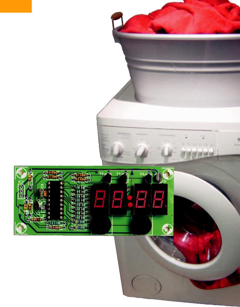
Timer Switch
for Washing Machine
Switching on command
Goswin Visschers
Many households have a utility supply separate day/night tariff, where the board delivers cheaper power during the and weekends. It can be economical to example, the washing machine at that
is, as long as you’re actually there to turn the right time, because modern electronically
washing machines cannot be delayed with a simple timer switch. But with a handful of components you can build yourself a circuit than can actually do this!
66 |
elektor electronics - 1/2006 |
|
|
|
+5V |
|
|
|
|
|
|
|
|
|
|
|
|
|
|
|
|
|
|
|
|
|
|
|
|
|
|
|
|
|
|
|
|
|
|
|
|
|
|
|
|
|
|
|
|
|
|
|
|
|
|
|
|
|
|
T5 |
|
|
|
|
|
|
|
|
|
R17 |
|
|
|
|
|
|
|
|
|
|
|
|
|
|
T4 |
|
|
|
|
|
|
|
|
|
|
|
|
|
10k |
|
|
|
|
|
|
|
|
|
|
|
|
|
|
|
|
|
|
|
BC558 |
||
|
|
|
|
|
|
|
R16 |
|
|
|
|
|
|
|
|
|
|
|
|
|
|
|
|
|
|
|
|||
|
|
|
|
|
|
|
10k |
|
|
|
|
|
|
|
|
|
T3 |
|
|
|
|
|
|
|
|
|
|
|
|
|
|
|
|
|
|
|
R15 |
|
|
|
|
|
|
|
|
|
|
|
|
|
|
|
|
|
|
|
|
||
|
|
|
|
|
|
|
10k |
|
|
|
|
|
|
|
|
|
|
|
|
|
|
BC558 |
|
|
|
|
|
||
|
|
|
|
|
|
|
R14 |
|
|
|
|
|
|
|
|
|
|
|
|
|
|
|
|
|
|
|
|||
|
|
|
|
|
|
|
10k |
|
|
|
|
T2 |
|
|
|
|
|
|
|
|
|
|
|
|
|
|
|
|
|
|
|
|
|
|
|
|
|
|
|
|
|
|
|
|
|
|
|
|
|
|
|
|
|
|
|
|
|
||
|
|
|
|
|
|
|
C6 |
|
|
|
|
|
|
|
|
|
|
BC558 |
|
|
|
|
|
|
|
|
|
|
|
R3 |
|
R2 |
|
|
|
|
|
|
|
|
|
|
|
|
|
|
|
|
|
|
|
|
|
|
|
|
|
|
|
|
|
|
|
|
|
|
|
|
|
|
|
|
|
|
|
|
D8 |
|
|
|
|
|
|
|
|
|
|
||
10k |
|
100 Ω |
|
|
|
|
|
|
|
|
|
|
BC558 |
|
|
|
|
|
|
|
|
|
|
|
|
|
|
||
|
|
|
|
|
100n |
|
|
|
|
|
|
|
|
|
|
|
|
|
|
|
|
|
|
|
|
||||
|
|
14 |
|
|
|
|
|
|
|
|
|
|
|
|
|
|
|
|
|
|
|
|
|
|
|
|
|||
|
|
|
|
|
|
|
LD1 |
|
|
|
LD2 |
|
|
|
LD3 |
|
|
|
LD4 |
|
|
|
|||||||
|
|
|
|
|
|
|
|
|
|
3 |
14 |
|
3 |
14 |
|
3 |
14 |
|
3 |
14 |
|
||||||||
|
|
4 |
MCLR |
|
RB0 |
6 |
150 Ω |
R4 |
1 |
a |
CA |
CA |
1 |
a |
CA |
CA |
1 |
a |
CA |
CA |
1 |
a |
CA |
CA |
|
||||
|
|
|
|
|
|
2 |
|
|
|
2 |
|
|
|
2 |
|
|
|
2 |
|
|
|
|
|||||||
|
|
|
|
|
RB1 |
7 |
150 Ω R5 |
f |
|
|
|
f |
|
|
|
f |
|
|
|
f |
|
|
|
|
|||||
|
|
17 |
RA0 |
IC2 |
RB2 |
8 |
150 Ω R7 |
13 |
b |
|
|
|
13 |
b |
|
|
|
13 |
b |
|
|
|
13 |
b |
|
|
|
|
|
|
|
18 |
RA1 |
|
RB3 |
9 |
150 Ω R6 |
11 |
g |
|
|
|
11 |
g |
|
|
|
11 |
g |
|
|
|
11 |
g |
|
|
|
|
|
|
|
1 |
RA2 |
|
RB4 |
10 |
150 Ω R10 10 |
c |
|
|
|
10 |
c |
|
|
|
10 |
c |
|
|
|
10 |
c |
|
|
|
|
||
|
|
2 |
RA3 |
|
RB5 |
11 |
150 Ω R9 |
7 |
e |
|
|
|
7 |
e |
|
|
|
7 |
e |
|
|
|
7 |
e |
|
|
|
|
|
|
|
3 |
RA4 PIC16F84 |
RB6 |
12 |
150 Ω R12 |
8 |
d |
|
|
|
8 |
d |
|
|
|
8 |
d |
|
|
|
8 |
d |
|
|
|
|
||
R18 |
R8 |
R11 |
|
|
RB7 |
13 |
150 Ω R13 |
6 |
dp |
|
|
6 |
dp |
|
|
|
6 |
dp |
|
|
|
6 |
dp |
|
|
|
|
||
Ω |
Ω |
Ω |
OSC2 |
OSC1 |
|
|
|
|
|
|
|
MAN4710A |
|
|
|
MAN4710A |
|
|
|
MAN4710A |
|
|
|
MAN4710A |
|
||||
470 |
470 |
470 |
|
|
|
|
|
|
|
|
|
|
D7 |
|
|
|
|
|
|
||||||||||
15 |
16 |
5 |
|
|
|
|
|
|
|
|
|
|
|
|
|
|
|
||||||||||||
|
|
|
|
|
|
|
|
|
|
|
|
|
|
|
|
|
|
|
|
|
|
|
|
||||||
|
|
|
|
X1 |
|
|
|
|
|
|
|
|
|
|
|
|
|
|
|
|
|
|
|
|
|
|
|
|
|
S1 |
|
S2 |
|
|
|
|
|
|
|
|
|
|
|
|
|
|
|
|
|
|
|
|
|
|
|
|
|
|
|
|
|
|
C4 |
C5 |
|
|
|
|
|
|
|
|
|
|
|
|
|
|
|
|
|
|
|
|
|
|
|
|
|
HOURS |
|
MINUTES |
|
|
|
|
|
|
|
|
|
|
|
|
|
|
|
|
|
|
|
|
|
|
|
|
|
|
|
|
|
100p |
100p |
|
|
|
|
|
|
|
|
|
|
|
|
|
|
|
|
|
|
|
|
|
|
|
|
|
|
|
|
|
X1 = 32.768kHz |
|
|
|
|
|
|
|
|
|
|
|
|
|
|
|
|
|
|
|
|
|
|
|
|
|
|
|
|
|
|
|
|
|
|
|
|
|
|
|
IC1 |
|
|
|
|
+5V |
|
|
|
|
|
|
|
|
|
|
|
|
|
|
|
|
|
|
|
|
|
|
|
|
|
|
|
|
|
|
|
|
|
|
|
|
|
|
|
|
|
|
|
|
|
|
|
|
|
|
|
|
|
|
78L05 |
|
|
|
|
|
|
|
|
|
|
|
|
|
|
||
|
F1 |
TR1 |
|
|
|
|
|
|
|
|
|
|
|
|
|
|
|
|
|
|
|
|
|
|
|
|
|
|
|
|
|
|
|
|
|
|
|
|
|
|
|
|
|
|
|
|
|
+5V |
|
|
|
|
+5V |
|
|
|
|
||
|
|
|
|
|
|
|
|
|
|
|
|
|
|
|
|
|
|
|
|
|
|
|
|
|
|
|
|||
K1 |
100mA |
|
|
|
|
RE1 |
|
D1 |
|
C1 |
C2 |
|
|
|
C3 |
D2 |
|
|
|
|
|
|
|
|
|
D5 |
D3 |
||
|
|
|
|
|
|
|
|
|
|
D1...D6 = |
1N4148 |
|
|
|
|
||||||||||||||
|
|
|
|
|
|
|
|
|
|
|
|
|
|
|
|
|
|
|
|
|
|||||||||
|
|
9V |
|
|
|
|
|
|
|
|
|
|
|
|
|
|
|
|
|
|
|
|
|
|
|||||
|
|
|
|
|
|
|
|
|
|
|
|
|
|
|
|
|
|
|
|
|
|
|
|
|
|
|
|
|
|
|
|
|
|
|
|
|
|
|
|
|
|
47µ |
100n |
|
|
|
100n |
|
|
|
|
|
|
|
|
|
|
|
|
230V |
|
|
|
B1 |
|
|
|
|
|
|
|
16V |
|
|
|
|
|
|
K3 |
|
|
K3' |
|
|
|
|
|
|
|
|
|
|
|
|
|
1N4148 |
|
|
|
|
|
|
|
|
|
|
|
|
|
|
|
|
|||||||
|
|
|
|
|
|
|
|
|
|
|
|
|
|
|
|
|
|
|
|
|
OUT |
|
|
||||||
|
|
|
|
|
|
|
T1 |
|
|
|
|
|
|
|
|
|
|
|
|
|
|
|
|
|
|
||||
|
|
|
|
|
|
|
|
|
R1 |
|
|
|
|
|
|
|
|
|
|
|
|
|
|
|
|
|
|
||
|
|
|
|
|
|
|
|
|
|
|
|
|
|
|
|
|
OUT |
|
|
|
|
|
|
|
|
|
|
|
|
|
|
|
|
|
|
|
|
|
|
|
1k |
|
|
|
|
|
|
|
|
|
|
|
|
|
|
|
|
||
|
|
|
|
|
|
|
|
|
|
|
|
|
|
|
|
D4 |
|
|
|
|
|
|
|
|
|
|
D6 |
||
|
|
|
|
|
|
|
|
|
|
|
|
|
|
|
|
|
|
|
|
|
|
|
|
|
|
|
|
||
|
|
|
B40C1500R |
|
|
|
BC547 |
|
|
|
|
|
|
|
|
|
GND |
|
|
|
|
GND |
|
|
|||||
|
K2 |
|
|
|
|
|
|
|
|
|
|
|
|
|
|
|
|
|
|
|
|
|
|||||||
|
|
|
|
|
|
|
|
|
|
|
|
|
|
|
|
|
|
|
|
|
|
|
|
|
|
|
|
|
|
START |
|
|
|
|
|
|
|
|
|
|
|
|
|
|
|
|
|
|
|
|
|
|
|
|
|
|
|
|
|
|
|
|
|
|
|
|
|
|
|
|
|
|
|
|
|
|
|
|
|
|
|
|
|
|
|
|
|
050058 - 11 |
|
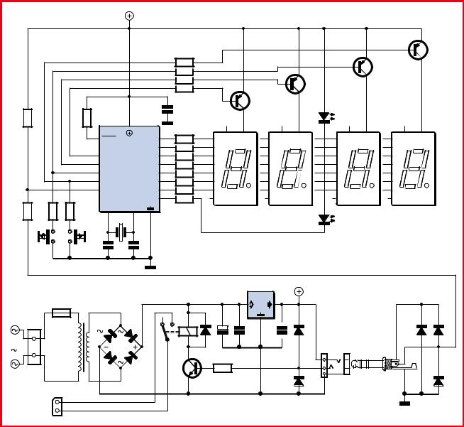
Figure 1. The schematic for the timer switch consists of two parts, each of which has its own PCB.
This electronic timer switch starts the washing machine by bridging the pushbutton for the start button for a few seconds using a relay. This does, however, require a small change to the washing machine. It is necessary to solder a wire to each side of the start pushbutton on the washing machine control PCB and to connect these wires to the relay contacts.
The timer switch is built on two circuit boards. The power supply PCB with the relay will go inside the washing machine. The PCB with the microcontroller is mounted in a separate enclosure and is attached to the outside of the washing machine.
The connection between the two PCBs (switch signal and power supply) is
1/2006 - elektor electronics
achieved with a 3.5-mm stereo jack plug and mating socket.
The design
Figure 1 shows the schematic for the complete timer switch. The top section is the control part with a PIC16F84 and four seven-segment displays. The bottom section is the power supply and switching part that will be built into the washing machine.
Power supply PCB
The power supply PCB is a straightforward design. A small mains transformer provides an AC voltage of about 9 V. The direct voltage resulting from rectification and filtering is regulated
by IC1 into a supply voltage of 5 V for the entire circuit.
The relay, whose contacts bridge the start button, is energised with the aid of switching transistor T1. The purpose of diodes D2 and D4 is to protect the base of T1 when the jack plug is either connected or disconnected.
If the washing machine has an on/offswitch instead of a start button, then this switch can be bridged with a bigger relay instead (however, take note of the maximum power rating of the washing machine).
This also requires a small change to the software: after the washing machine has been switched on by the timer switch, the relay needs to remain energised until the clock is reset.
67
HANDS-ON HOME AUTOMATION
Control PCB
In this part of the timer switch, the objective was to use as few electronic parts as feasible and integrate as much functionality as possible into the microcontroller.
Diodes D3, D5 and D6 have the same purpose as D2 and D4, that is, protection for the ports when the jack plug is connected or disconnected.
X1 is a 32.768 kHz quartz crystal, the same type as those used in watches. This frequency is a power of two, which makes it easy to divide it down to a half second (half the time period of the colon).
The pins from the microcontroller are used as follows. Pins RB0 through to RB6 are used to drive the seven segments of the displays in multiplexed fashion. Resistors R4 to R13 limit the current through the LED-segments. Pin RB7 is for the colon (LEDs D7 and D8). Pins RA0 through RA3, via driver transistors T2 to T5, generate the multiplex drive signals for the displays. In addition, RA2 and RA3 are read once per cycle of the ‘main loop’ to test the state of the two pushbuttons S1 and S2.
In case you would like to modify the software yourself, it is possible to use RA0 and RA1 in the same manner as RA2 and RA3 and allow for two more pushbuttons.
RA4 is used to switch the relay via T1. Since this is an open-collector output, the purpose of R3 is to supply the drive current for T1.
Construction and Installation
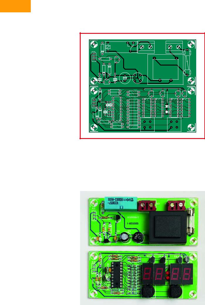
Figure 2 shows the PCB layout that has been designed for this timer switch. Here, the two parts are joined together, but normally the two PCBs will be mounted in different locations. The assembly of the PCBs is mostly routine, but don’t forget the three wire links on the control PCB.
The construction and installation of this circuit has already been mentioned at the start of this article. You can choose to keep the two parts completely separate. That is, the power supply PCB inside the washing machine and the control PCB outside. The front of the washing machine could be fitted with a jack socket for the interconnection with the control PCB. The control enclosure can then be fastened on the washing machine somewhere (for example with mag-
|
|
|
|
|
|
K2 |
K1 |
|
K3 |
D1 |
|
RE1 |
|
|
start |
230V~ |
|
|
|
|
|
|
||||
|
|
|
|
|
|
|||
|
R1 |
|
T1 |
050058-1 |
|
|
|
100mAT |
|
|
|
|
|
|
|||
|
|
|
(C)ELEKTOR |
|
|
|
||
|
|
|
|
|
|
|
||
|
|
|
|
050058-1 |
|
|
|
F1 |
|
D2 |
D4 |
C2 |
C1 |
B1 |
|
TR1 |
|
|
|
|
||||||
C3 |
|
|
|
|
|
|||
|
|
|
|
|
|
|
|
|
|
IC1 |
|
|
|
|
|
|
|
|
|
|
R15 |
R16 |
T2 |
T3 |
T4 |
|
|
D5 |
|
R14 |
|
|
|
|
|
K3’ |
|
R17 |
|
|
|
T5 |
||
|
|
|
|
|
||||
C4 |
C6 |
|
|
|
|
|
|
|
|
|
R7 |
|
|
D8 |
|
||
|
|
|
|
|
|
|
||
|
|
|
|
R6 |
LD1 |
LD2 |
LD3 |
LD4 |
|
|
|
IC2 |
R10 |
||||
|
|
|
R5 |
|||||
D6 |
|
|
R4 |
|||||
D3 |
|
|
|
|
|
|
||
|
|
R9 |
|
|
D7 |
|
||
|
|
|
|
|
|
|
||
|
C5 X1 |
|
R12 |
|
|
|
||
|
|
|
|
|
|
|||
|
R3 |
|
|
R13 |
|
|
|
|
|
|
R2 |
R8 |
S1 |
|
S2 |
|
|
|
|
|
|
|
||||
|
|
|
|
|
|
|||
|
|
|
R18 |
R11 |
|
|
|
|
Figure 2. The two PCBs are shown here joined together, but in practice each one will be mounted in a different location.
netic stickers). |
this is a much more challenging task |
It is also possible to fit the entire cir- |
because of the available space and the |
cuit inside the washing machine, but |
openings that are required for the front |
|
|
|
|
Figure 3. The prototype shown here differs slightly from the final printed circuit boards.
68 |
elektor electronics - 1/2006 |
COMPONENTS LIST
Resistors:
R1,R18 = 1kΩ
R2 = 100Ω
R4-R7,R9,R10,R12,R13 = 150Ω
R8,R11 = 470Ω
R3,R14-R17 = 10kΩ
Capacitors:
C1 = 47µF 16V radial
C2,C3,C6 = 100nF
C4,C5 = 100pF
Semiconductors:
B1 = B40C1500R bridge rectifier
(40V piv, 1.5A)
D1-D6 = 1N4148
D7,D8 = LED, red, 3mm diam. IC1 = 78L05
IC2 = PIC16F84, programmed, order code 050058-41
LD1-LD4 = 7-segment display, e.g. Fairchild type MAN4710A
T1 = BC547B
T2-T5 = BC558
Miscellaneous:
F1 = fuse, 100mAT (slow) with PCB mount holder
K1,K2 = 2-way PCB terminal block, lead pitch 7.5mm
K3,K3’ = 3.5mm stereo jack plug with socket
R1 = 12V relay (e.g. Siemens
V23057-12V)
S1,S2 = pushbutton (e.g., ITT D6-R-90) Tr1 = mains transformer, 230V
primary, secondary 9V @ 1VA (e.g. Block VB1,0/1/9)
X1 = 32.768kHz quartz crystal PCB, order code 050058-1
Disk, PIC source and hex code, order code 050058-11
panel. This is why the author chose for the solution with the jack socket.
Operation
The operation is extremely easy. After the circuit is switched on, four dashes are shown on the display (‘——‘).
With one pushbutton (S2) you can increase the minutes in steps of 10 minutes, with the other pushbutton (S1), the hours in steps of 1 hour. Once the buttons have not been pressed for 1 second, the timer will begin to count down automatically.
During the countdown, the time remaining is visible on the displays.
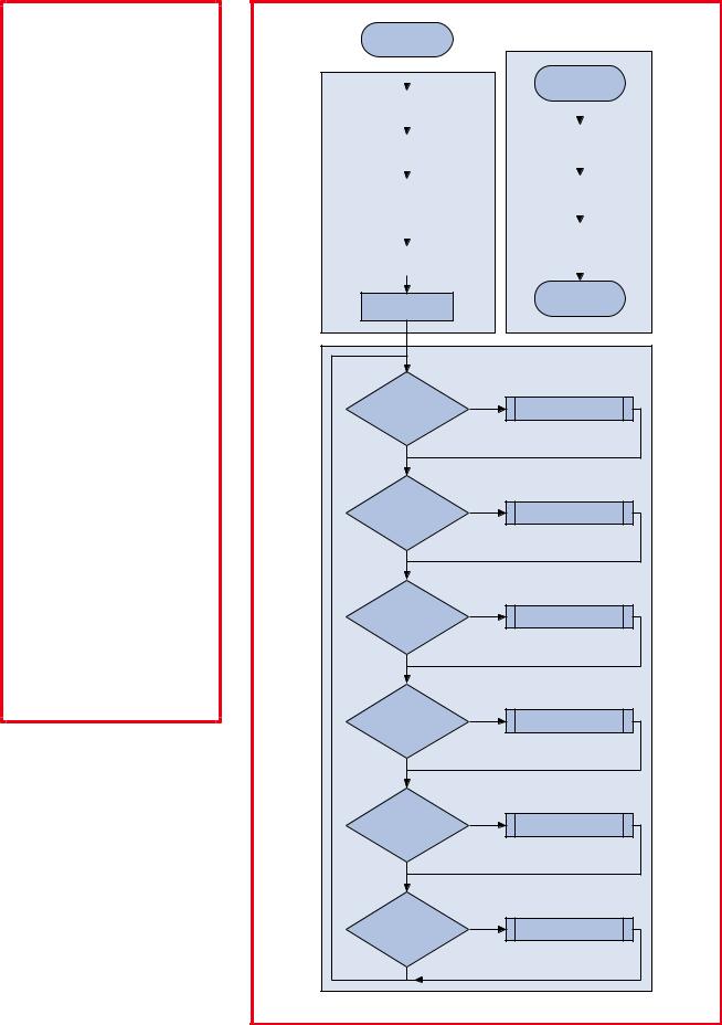
|
Init |
|
|
|
|
|
|||
|
|
|
|
|
|
Interrupt |
|||
|
|
|
|
|
|
||||
|
Clear timer register |
|
|
|
|
|
|
||
|
|
|
|
|
|
|
|||
|
|
|
|
|
|
|
|
|
|
|
|
|
|
|
|
|
|
|
|
|
|
|
|
|
|
Save contents of |
|||
|
Clear watchdog |
|
|
Status and W register |
|||||
|
|
|
|
|
|
|
|
|
|
|
|
|
|
|
|
|
|
|
|
|
Initialise: |
|
|
Set action bit 5 |
|
||||
data direction registers, |
|
|
|
|
|
||||
|
action register, |
|
|
|
|
|
|||
|
timer register |
|
|
|
|
|
|||
|
|
|
|
|
|
Restore contents of |
|||
|
|
|
|
|
|
||||
|
|
|
|
|
Status and W register |
||||
Clear clock registers and |
|||||||||
|
|
|
|
|
|||||
|
button hold registers |
|
|
|
|
|
|||
|
|
|
|
|
|
|
|
|
|
|
Return from |
|
Enable interrupts |
interrupt |
|
Test if |
|
|
deci hours |
Call deci_hour_out |
|
should be set on |
||
LED display |
|
|
Test if |
|
|
centi hours |
Call centi_hour_out |
|
should be set on |
||
LED display |
|
|
Test if |
|
|
deci minutes |
Call deci_min_out |
|
should be set on |
||
LED display |
|
|
Test if |
|
|
centi minutes |
Call centi_min_out |
|
should be set on |
||
LED display |
|
|
Test if |
|
|
button statusses |
Call read_but |
|
should be |
||
processed |
|
|
Test if |
|
|
clock registers |
Call upd_clk |
|
should be |
||
|
||
updated |
|
|
|
050058 - 12 |
Figure 4. This flowchart shows the design of the main program.
1/2006 - elektor electronics |
69 |

HANDS-ON HOME AUTOMATION
When the time is up, the relay is energised and the display is turned off. After the relay is turned off again, the four dashes reappear on the display. If both pushbuttons are pressed at the same time, the timer switch will be reset and the four dashes will appear on the display.
Software
The code in the microcontroller has been designed to be as general-pur- pose as possible, so that this circuit can be used for other applications by changing a few constants.
The code comprises two files: clock.asm that contains the machine code and clock.inc, which contains the constants and register definitions. These files are available free of charge from the Elektor Electronics website (and on floppy disk, order code 05005811, for those without access to the Internet).
The heart of the machine code file naturally consists of the main loop (lines 105 to 118).
The bits in the ‘action_reg’ register are tested in the ‘main loop’ in order to determine the next action (see comments in the code).
The seven-segment displays are driven in turn, after which the pushbuttons are tested. Then, depending on whether an interrupt has taken place, the time is updated.
If the output has to remain energised permanently, instead of momentarily, the ‘goto acti_time’ command has to be replaced with ‘return’.
A few constants can be changed:
active_time
Duration that the output is energised in half seconds. (not relevant if the output has to stay on permanently.)
hold_but_cyc
Number of cycles to wait before a button can be operated again.
Zero_led…Err_led
Bit values that display a number
on the seven-segment display. In the event the seven-segment
displays are connected differently, the numbers can be displayed correctly via Port B by suitably changing these values.
dub_dot_bit
Bit value which represents the location of the colon.
In this case the value is such that the two LEDs for the colon are driven via Port RB7.
setm_but and seth_but
Port numbers for Port A to which the minutes and hours pushbuttons are connected.
For further clarification, Figure 4 shows a flow chart of the main program. The charts for the various program parts referred to may be downloaded as a PDF file from the Elektor Electronics website.
You can find more details in the source code file supplied to us by the author.
(050058-1)
C O N S T R U C T I O N G U I D E L I N E S
Elektor Electronics (Publishing) does not provide parts and components other than PCBs, fornt panel foils and software on diskette or IC (not necessarily for all projects). Components are usually available form a number of retailers – see the adverts in the magazine.
Large and small values of components are indicated by means of one of the following prefixes :
E (exa) = 1018 |
a (atto) = 10–18 |
P (peta) = 1015 |
f (femto) = 10–15 |
T (tera) = 1012 |
p (pico) = 10–12 |
G (giga) = 109 |
n (nano) = 10–9 |
M (mega) = 106 |
µ (micro) = 10–6 |
k (kilo) = 103 |
m (milli) = 10–3 |
h (hecto) = 102 |
c (centi) = 10–2 |
da (deca) = 101 |
d (deci) = 10–1 |
In some circuit diagrams, to avoid confusion, but contrary to IEC and BS recommandations, the value of components is given by substituting the relevant prefix for the decimal point. For example,
3k9 = 3.9 kΩ 4µ7 = 4.7 µF
Unless otherwise indicated, the tolerance of resistors is ±5% and their rating is 1⁄3–1⁄2 watt. The working voltage of capacitors is ≥ 50 V.
In populating a PCB, always start with the smallest passive components, that is, wire bridges, resistors and small capacitors; and then IC sockets, relays, electrolytic and other large capacitors, and connectors. Vulnerable semiconductors and ICS should be done last.
Soldering. Use a 15–30 W soldering iron with a fine tip and tin with a resin core (60/40) Insert the terminals of components in the board, bend them slightly, cut them short, and solder: wait 1–2 seconds for the tin to flow smoothly and remove the iron. Do not overheat, particularly when soldering ICS and semiconductors. Unsoldering is best done with a suction iron or special unsoldering braid.
Faultfinding. If the circuit does not work, carefully compare the populated board with the published component layout and parts list. Are all the com-
ponents in the correct position? Has correct polarity been observed? Have the powerlines been reversed? Are all solder joints sound? Have any wire bridges been forgotten?
If voltage levels have been given on the circuit diagram, do those measured on the board match them – note that deviations up to ±10% from the specified values are acceptable.
Possible corrections to published projects are published from time to time in this magazine. Also, the readers letters column often contains useful comments/additions to the published projects.
The value of a resistor is indicated by a colour code as follows.
|
|
|
|
|
|
|
|
|
|
|
|
|
|
|
|
|
|
|
|
|
|
|
|
|
|
|
|
|
|
|
|
|
|
|
|
|
|
|
|
|
|
|
|
|
|
|
|
|
|
|
|
|
|
|
|
|
|
|
|
|
|
|
|
|
|
|
|
|
color |
|
1st digit |
|
2nd digit |
mult. factor |
tolerance |
||||||||||||||||
|
|
|
|
|
|
|
|
|
|
|
|
|
|
|
||||||||
black |
|
– |
0 |
|
|
|
|
|
|
– |
|
|
– |
|||||||||
brown |
1 |
|
|
|
|
|
1 |
|
× 101 |
±1% |
||||||||||||
red |
2 |
|
|
|
|
|
2 |
|
× 102 |
±2% |
||||||||||||
orange |
3 |
|
|
|
|
|
3 |
|
× 103 |
|
|
– |
||||||||||
yellow |
4 |
|
|
|
|
|
4 |
|
× 104 |
|
|
– |
||||||||||
green |
5 |
|
|
|
|
|
5 |
|
× 105 |
±0,5% |
||||||||||||
blue |
6 |
|
|
|
|
|
6 |
|
× 106 |
|
|
– |
||||||||||
violet |
7 |
|
|
|
|
|
7 |
|
|
|
|
|
|
– |
|
|
– |
|||||
grey |
8 |
|
|
|
|
|
8 |
|
|
|
|
|
|
– |
|
|
– |
|||||
white |
9 |
|
|
|
|
|
9 |
|
|
|
|
|
|
– |
|
|
– |
|||||
gold |
|
– |
|
|
|
– |
|
|
|
|
× 10–1 |
±5% |
||||||||||
silver |
|
– |
|
|
|
– |
|
|
|
|
× 10–2 |
±10% |
||||||||||
none |
|
– |
|
|
|
– |
|
|
|
|
|
– |
±20% |
|||||||||
Examples:
brown-red-brown-gold = 120 Ω, 5% yellow-violet-orange-gold = 47 kΩ, 5%
70 |
elektor electronics - 1/2006 |