

- •LabVIEW Measurements Manual
- •Worldwide Technical Support and Product Information
- •National Instruments Corporate Headquarters
- •Worldwide Offices
- •Important Information
- •Warranty
- •Copyright
- •Trademarks
- •WARNING REGARDING USE OF NATIONAL INSTRUMENTS PRODUCTS
- •Contents
- •About This Manual
- •Conventions
- •Related Documentation
- •History of Instrumentation
- •What Is Virtual Instrumentation?
- •DAQ Devices versus Special-Purpose Instruments
- •How Do Computers Talk to DAQ Devices?
- •Role of Software
- •How Do Programs Talk to Instruments?
- •Overview
- •Installing and Configuring Your Hardware
- •Measurement & Automation Explorer (Windows)
- •NI-DAQ Configuration Utility (Macintosh)
- •NI-488.2 Configuration Utility (Macintosh)
- •Configuring Your DAQ Channels
- •Assigning VISA Aliases and IVI Logical Names
- •Configuring Serial Ports on Macintosh
- •Configuring Serial Ports on UNIX
- •Example DMM Measurements
- •How to Measure DC Voltage
- •Single-Point Acquisition Example
- •Averaging a Scan Example
- •How to Measure AC Voltage
- •How to Measure Current
- •How to Measure Resistance
- •How to Measure Temperature
- •Example Oscilloscope Measurements
- •How to Measure Maximum, Minimum, and Peak-to-Peak Voltage
- •How to Measure Frequency and Period of a Repetitive Signal
- •Measuring Frequency and Period Example
- •Finding Common DAQ Examples
- •Finding the Data Acquisition VIs in LabVIEW
- •DAQ VI Organization
- •Easy VIs
- •Intermediate VIs
- •Utility VIs
- •Advanced VIs
- •Polymorphic DAQ VIs
- •VI Parameter Conventions
- •Default and Current Value Conventions
- •The Waveform Control
- •Waveform Control Components
- •Using the Waveform Control
- •Extracting Waveform Components
- •Waveform Data on the Front Panel
- •Channel, Port, and Counter Addressing
- •DAQ Channel Name Control
- •Channel Name Addressing
- •Channel Number Addressing
- •Limit Settings
- •Other DAQ VI Parameters
- •Error Handling
- •Organization of Analog Data
- •Where You Should Go Next
- •Defining Your Signal
- •Grounded Signal Sources
- •Floating Signal Sources
- •Choosing Your Measurement System
- •Considerations for Selecting Analog Input Settings
- •Channel Addressing with the AMUX-64T
- •Important Terms You Should Know
- •Single-Point Acquisition
- •Single-Channel, Single-Point Analog Input
- •Multiple-Channel, Single-Point Analog Input
- •Using Analog Input/Output Control Loops
- •Using Software-Timed Analog I/O Control Loops
- •Using Hardware-Timed Analog I/O Control Loops
- •Improving Control Loop Performance
- •Buffered Waveform Acquisition
- •Acquiring a Single Waveform
- •Acquiring Multiple Waveforms
- •Simple-Buffered Analog Input Examples
- •Simple-Buffered Analog Input with Graphing
- •Simple-Buffered Analog Input with Multiple Starts
- •Using Circular Buffers to Access Your Data during Acquisition
- •Continuously Acquiring Data from Multiple Channels
- •Controlling Your Acquisition with Triggers
- •Hardware Triggering
- •Digital Triggering
- •Analog Triggering
- •Software Triggering
- •Conditional Retrieval Examples
- •Letting an Outside Source Control Your Acquisition Rate
- •Externally Controlling Your Channel Clock
- •Externally Controlling Your Scan Clock
- •Externally Controlling the Scan and Channel Clocks
- •Single-Point Output
- •Buffered Analog Output
- •Single-Point Generation
- •Single-Immediate Updates
- •Multiple-Immediate Updates
- •Waveform Generation (Buffered Analog Output)
- •Buffered Analog Output
- •Circular-Buffered Analog Output Examples
- •Letting an Outside Source Control Your Update Rate
- •Externally Controlling Your Update Clock
- •Supplying an External Test Clock from Your DAQ Device
- •Software Triggered
- •Hardware Triggered
- •Using Lab/1200 Boards
- •Types of Digital Acquisition/Generation
- •Knowing Your Digital I/O Chip
- •653X Family
- •E Series Family
- •8255 Family
- •Using Channel Names
- •Immediate I/O Using the Easy Digital VIs
- •653X Family
- •E Series Family
- •8255 Family
- •Immediate I/O Using the Advanced Digital VIs
- •653X Family
- •E Series Family
- •8255 Family
- •Handshaking
- •Handshaking Lines
- •653X Family
- •8255 Family
- •Digital Data on Multiple Ports
- •653X Family
- •8255 Family
- •Types of Handshaking
- •Nonbuffered Handshaking
- •653X Family
- •8255 Family
- •Buffered Handshaking
- •Simple-Buffered Handshaking
- •Iterative-Buffered Handshaking
- •Circular-Buffered Handshaking
- •Pattern I/O
- •Finite Pattern I/O
- •Finite Pattern I/O without Triggering
- •Finite Pattern I/O with Triggering
- •Continuous Pattern I/O
- •What Is Signal Conditioning?
- •Amplification
- •Linearization
- •Transducer Excitation
- •Isolation
- •Filtering
- •Hardware and Software Setup for Your SCXI System
- •SCXI Operating Modes
- •Multiplexed Mode for Analog Input Modules
- •Multiplexed Mode for Analog Output Modules
- •Multiplexed Mode for Digital and Relay Modules
- •Parallel Mode for Analog Input Modules
- •Parallel Mode for the SCXI-1200 (Windows)
- •Parallel Mode for Digital Modules
- •SCXI Software Installation and Configuration
- •Special Programming Considerations for SCXI
- •SCXI Channel Addressing
- •SCXI Gains
- •SCXI Settling Time
- •Common SCXI Applications
- •Measuring Temperature with Thermocouples
- •Amplifier Offset
- •VI Examples
- •Measuring Temperature with RTDs
- •Measuring Pressure with Strain Gauges
- •Analog Output Application Example
- •Digital Input Application Example
- •Digital Output Application Example
- •Multi-Chassis Applications
- •Calibrating SCXI Modules
- •SCXI Calibration Methods for Signal Acquisition
- •One-Point Calibration
- •Two-Point Calibration
- •Calibrating SCXI Modules for Signal Generation
- •Knowing the Parts of Your Counter
- •Knowing Your Counter Chip
- •TIO-ASIC
- •Generating a Square Pulse
- •TIO-ASIC, DAQ-STC, and Am9513
- •Generating a Single Square Pulse
- •TIO-ASIC, DAQ-STC, Am9513
- •Generating a Pulse Train
- •Generating a Continuous Pulse Train
- •Generating a Finite Pulse Train
- •Counting Operations When All Your Counters Are Used
- •Knowing the Accuracy of Your Counters
- •Stopping Counter Generations
- •Measuring Pulse Width
- •Measuring a Pulse Width
- •Determining Pulse Width
- •Controlling Your Pulse Width Measurement
- •TIO-ASIC, DAQ-STC, or Am9513
- •Buffered Pulse and Period Measurement
- •Increasing Your Measurable Width Range
- •TIO-ASIC, DAQ-STC, Am9513
- •Connecting Counters to Measure Frequency and Period
- •TIO-ASIC, DAQ-STC, Am9513
- •TIO-ASIC, DAQ-STC
- •TIO-ASIC, DAQ-STC, Am9513
- •TIO-ASIC, DAQ-STC
- •TIO-ASIC, DAQ-STC, Am9513
- •Counting Signal Highs and Lows
- •Connecting Counters to Count Events and Time
- •Counting Events
- •TIO-ASIC, DAQ-STC
- •Counting Elapsed Time
- •TIO-ASIC, DAQ-STC
- •Dividing Frequencies
- •TIO-ASIC or DAQ-STC
- •The Importance of Data Analysis
- •Data Sampling
- •Sampling Signals
- •Sampling Considerations
- •Why Do You Need Anti-Aliasing Filters?
- •Why Use Decibels?
- •What Is the DC Level of a Signal?
- •What Is the RMS Level of a Signal?
- •Averaging to Improve the Measurement
- •DC Overlapped with Single Tone
- •Defining the Equivalent Number of Digits
- •DC Plus Sine Tone
- •Windowing to Improve DC Measurements
- •RMS Measurements Using Windows
- •Using Windows with Care
- •Rules for Improving DC and RMS Measurements
- •RMS Levels of Specific Tones
- •Frequency vs. Time Domain
- •Aliasing
- •FFT Fundamentals
- •Fast FFT Sizes
- •Magnitude and Phase
- •Windowing
- •Averaging to Improve the Measurement
- •Equations for Averaging
- •RMS Averaging
- •Vector Averaging
- •Peak Hold
- •Single-Channel Measurements—FFT, Power Spectrum
- •Dual-Channel Measurements—Frequency Response
- •What Is Distortion?
- •Application Areas
- •Harmonic Distortion
- •Total Harmonic Distortion
- •SINAD
- •Setting Up an Automated Test System
- •Specifying a Limit
- •Specifying a Limit Using a Formula
- •Limit Testing
- •Applications
- •Modem Manufacturing Example
- •Digital Filter Design Example
- •Pulse Mask Testing Example
- •What Is Filtering?
- •Advantages of Digital Filtering over Analog Filtering
- •Common Digital Filters
- •Ideal Filters
- •Practical (Nonideal) Filters
- •The Transition Band
- •Passband Ripple and Stopband Attenuation
- •FIR Filters
- •IIR Filters
- •Butterworth Filters
- •Chebyshev Filters
- •Chebyshev II or Inverse Chebyshev Filters
- •Elliptic (or Cauer) Filters
- •Bessel Filters
- •Choosing and Designing a Digital Filter
- •Common Test Signals
- •Multitone Generation
- •Crest Factor
- •Phase Generation
- •Swept Sine versus Multitone
- •Noise Generation
- •How Do You Use LabVIEW to Control Instruments?
- •Where Should You Go Next for Instrument Control?
- •Installing Instrument Drivers
- •Where Can I Get Instrument Drivers?
- •Where Should I Install My LabVIEW Instrument Driver?
- •Organization of Instrument Drivers
- •Kinds of Instrument Drivers
- •Inputs and Outputs Common to Instrument Driver VIs
- •Resource Name/Instrument Descriptor
- •Error In/Error Out Clusters
- •Verifying Communication with Your Instrument
- •Running the Getting Started VI Interactively
- •Verifying VISA Communication
- •What Is VISA?
- •Writing a Simple VISA Application
- •Using VISA Properties
- •Using the Property Node
- •Serial
- •GPIB
- •Using VISA Events
- •Types of Events
- •Handling GPIB SRQ Events Example
- •Advanced VISA
- •Opening a VISA Session
- •Closing a VISA Session
- •Locking
- •Shared Locking
- •String Manipulation Techniques
- •How Instruments Communicate
- •Building Strings
- •Removing Headers
- •Waveform Transfers
- •ASCII Waveforms
- •1-Byte Binary Waveforms
- •2-Byte Binary Waveforms
- •Serial Port Communication
- •How Fast Can I Transmit Data over the Serial Port?
- •Serial Hardware Overview
- •Your System
- •GPIB Communications
- •Controllers, Talkers, and Listeners
- •Hardware Specifications
- •VXI (VME eXtensions for Instrumentation)
- •VXI Hardware Components
- •VXI Configurations
- •PXI Modular Instrumentation
- •Computer-Based Instruments
- •Glossary
- •Index
- •Numbers
- •Figures
- •Figure 2-1. DAQ System Components
- •Figure 4-1. Simple Data Acquisition System
- •Figure 4-2. Wind Speed
- •Figure 4-3. Anemometer Wiring
- •Figure 4-4. Measuring Voltage and Scaling to Wind Speed
- •Figure 4-5. Measuring Wind Speed Using DAQ Named Channels
- •Figure 4-6. DAQ System for Measuring Wind Speed with Averaging
- •Figure 4-7. Wind Speed
- •Figure 4-8. Average Wind Speed Using DAQ Named Channels
- •Figure 4-9. Data Acquisition System for Vrms
- •Figure 4-10. Sinusoidal Voltage
- •Figure 4-11. Vrms Using DAQ Named Channels
- •Figure 4-12. Instrument Control System for Vrms
- •Figure 4-13. Vrms Using an Instrument
- •Figure 4-14. Data Acquisition System for Current
- •Figure 4-15. Current Loop Wiring
- •Figure 4-16. Linear Relationship between Tank Level and Current
- •Figure 4-17. Measuring Fluid Level Without DAQ Named Channels
- •Figure 4-18. Measuring Fluid Level Using DAQ Named Channels
- •Figure 4-19. Instrument Control System for Resistance
- •Figure 4-20. Measuring Resistance Using an Instrument
- •Figure 4-21. Simple Temperature System
- •Figure 4-22. Thermocouple Wiring
- •Figure 4-23. Measuring Temperature Using DAQ Named Channels
- •Figure 4-24. Data Acquisition System for Minimum, Maximum, Peak-to-Peak
- •Figure 4-25. Measuring Minimum, Maximum, and Peak-to-Peak Voltages
- •Figure 4-26. Instrument Control System for Peak-to-Peak Voltage
- •Figure 4-27. Measuring Peak-to-Peak Voltage Using an Instrument
- •Figure 4-28. Measuring Frequency and Period
- •Figure 4-29. Measuring Frequency Using an Instrument
- •Figure 4-30. Lowpass Filter
- •Figure 4-31. Measuring Frequency after Filtering
- •Figure 4-32. Front Panel IIR Filter Specifications
- •Figure 4-33. Measuring Frequency after Filtering Using an Instrument
- •Figure 5-1. Analog Input VI Palette Organization
- •Figure 5-2. Polymorphic DAQ VI Shortcut Menu
- •Figure 5-3. LabVIEW Context Help Window Conventions
- •Figure 5-4. Waveform Control
- •Figure 5-5. Using the Waveform Data Type
- •Figure 5-6. Single-Point Example
- •Figure 5-7. Using the Waveform Control with Analog Output
- •Figure 5-8. Extracting Waveform Components
- •Figure 5-9. Waveform Graph
- •Figure 5-10. Channel Controls
- •Figure 5-11. Channel String Array Controls
- •Figure 5-12. Limit Settings, Case 1
- •Figure 5-13. Limit Settings, Case 2
- •Figure 5-14. Wiring the iteration Input
- •Figure 5-15. LabVIEW Error In and Error Out Error Clusters
- •Figure 5-16. Example of a Basic 2D Array
- •Figure 5-17. 2D Array in Column Major Order
- •Figure 5-18. Extracting a Single Channel from a Column Major 2D Array
- •Figure 5-19. Analog Output Buffer 2D Array
- •Figure 6-1. Types of Analog Signals
- •Figure 6-2. Grounded Signal Sources
- •Figure 6-3. Floating Signal Sources
- •Figure 6-4. The Effects of Resolution on ADC Precision
- •Figure 6-5. The Effects of Range on ADC Precision
- •Figure 6-6. The Effects of Limit Settings on ADC Precision
- •Figure 6-7. 8-Channel Differential Measurement System
- •Figure 6-8. Common-Mode Voltage
- •Figure 6-9. 16-Channel RSE Measurement System
- •Figure 6-10. 16-Channel NRSE Measurement System
- •Figure 6-12. Using the Intermediate VIs for a Basic Non-Buffered Application
- •Figure 6-13. Acquiring and Graphing a Single Waveform
- •Figure 6-15. Using the Intermediate VIs to Acquire Multiple Waveforms
- •Figure 6-16. Simple Buffered Analog Input Example
- •Figure 6-17. Writing to a Spreadsheet File after Acquisition
- •Figure 6-18. How a Circular Buffer Works
- •Figure 6-19. Basic Circular-Buffered Analog Input Using the Intermediate VIs
- •Figure 6-20. Diagram of a Digital Trigger
- •Figure 6-21. Digital Triggering with Your DAQ Device
- •Figure 6-22. Diagram of an Analog Trigger
- •Figure 6-23. Analog Triggering with Your DAQ Device
- •Figure 6-24. Timeline of Conditional Retrieval
- •Figure 6-25. The AI Read VI Conditional Retrieval Cluster
- •Figure 6-26. Channel and Scan Intervals Using the Channel Clock
- •Figure 6-27. Round-Robin Scanning Using the Channel Clock
- •Figure 6-28. Example of a TTL Signal
- •Figure 6-29. Acquiring Data with an External Scan Clock
- •Figure 6-30. Controlling the Scan and Channel Clock Simultaneously
- •Figure 7-1. Waveform Generation Using the AO Waveform Gen VI
- •Figure 7-2. Waveform Generation Using Intermediate VIs
- •Figure 7-3. Circular Buffered Waveform Generation Using Intermediate VIs
- •Figure 8-1. Digital Ports and Lines
- •Figure 8-2. Connecting Signal Lines for Digital Input
- •Figure 8-3. Connecting Signal Lines for Digital Output
- •Figure 9-1. Common Types of Transducers/Signals and Signal Conditioning
- •Figure 9-3. SCXI System
- •Figure 9-4. Components of an SCXI System
- •Figure 9-5. SCXI Chassis
- •Figure 9-6. Measuring a Single Module with the Acquire and Average VI
- •Figure 9-7. Measuring Temperature Sensors Using the Acquire and Average VI
- •Figure 9-8. Continuously Acquiring Data Using Intermediate VIs
- •Figure 9-9. Measuring Temperature Using Information from the DAQ Channel Wizard
- •Figure 9-10. Measuring Temperature Using the Convert RTD Reading VI
- •Figure 9-11. Half-Bridge Strain Gauge
- •Figure 9-12. Measuring Pressure Using Information from the DAQ Channel Wizard
- •Figure 9-13. Inputting Digital Signals through an SCXI Chassis Using Easy Digital VIs
- •Figure 9-14. Outputting Digital Signals through an SCXI Chassis Using Easy Digital VIs
- •Figure 9-15. Ideal versus Actual Reading
- •Figure 10-1. Counter Gating Modes
- •Figure 10-2. Wiring a 7404 Chip to Invert a TTL Signal
- •Figure 10-3. Pulse Duty Cycles
- •Figure 10-4. Positive and Negative Pulse Polarity
- •Figure 10-5. Pulses Created with Positive Polarity and Toggled Output
- •Figure 10-6. Phases of a Single Negative Polarity Pulse
- •Figure 10-7. Physical Connections for Generating a Square Pulse
- •Figure 10-8. External Connections Diagram from the Front Panel of Delayed Pulse (8253) VI
- •Figure 10-9. Physical Connections for Generating a Continuous Pulse Train
- •Figure 10-10. External Connections Diagram from the Front Panel of Cont Pulse Train (8253) VI
- •Figure 10-11. Physical Connections for Generating a Finite Pulse Train
- •Figure 10-12. External Connections Diagram from the Front Panel of Finite Pulse Train (8253) VI
- •Figure 10-13. Uncertainty of One Timebase Period
- •Figure 10-14. Using the Generate Delayed Pulse and Stopping the Counting Operation
- •Figure 10-15. Stopping a Generated Pulse Train
- •Figure 10-16. Counting Input Signals to Determine Pulse Width
- •Figure 10-17. Physical Connections for Determining Pulse Width
- •Figure 10-18. Measuring Pulse Width with Intermediate VIs
- •Figure 10-19. Measuring Square Wave Frequency
- •Figure 10-20. Measuring a Square Wave Period
- •Figure 10-21. External Connections for Frequency Measurement
- •Figure 10-22. External Connections for Period Measurement
- •Figure 10-23. Frequency Measurement Example Using Intermediate VIs
- •Figure 10-24. Measuring Period Using Intermediate Counter VIs
- •Figure 10-25. External Connections for Counting Events
- •Figure 10-26. External Connections for Counting Elapsed Time
- •Figure 10-27. External Connections to Cascade Counters for Counting Events
- •Figure 10-28. External Connections to Cascade Counters for Counting Elapsed Time
- •Figure 10-29. Wiring Your Counters for Frequency Division
- •Figure 10-30. Programming a Single Divider for Frequency Division
- •Figure 11-1. Raw Data
- •Figure 11-2. Processed Data
- •Figure 11-3. Analog Signal and Corresponding Sampled Version
- •Figure 11-4. Aliasing Effects of an Improper Sampling Rate
- •Figure 11-5. Actual Signal Frequency Components
- •Figure 11-6. Signal Frequency Components and Aliases
- •Figure 11-7. Effects of Sampling at Different Rates
- •Figure 11-8. Ideal versus Practical Anti-Alias Filter
- •Figure 12-1. DC Level of a Signal
- •Figure 12-2. Instantaneous DC Measurements
- •Figure 12-3. DC Signal Overlapped with Single Tone
- •Figure 12-4. Digits vs Measurement Time for 1 VDC Signal with 0.5 Single Tone
- •Figure 12-5. Digits vs Measurement Time for DC+Tone Using Hann Window
- •Figure 12-6. Digits vs Measurement Time for DC+Tone Using LSL Window
- •Figure 12-7. Digits vs Measurement Time for RMS Measurements
- •Figure 13-1. Signal Formed by Adding Three Frequency Components
- •Figure 13-2. FFT Transforms Time-Domain Signals into the Frequency Domain
- •Figure 13-3. Periodic Waveform Created from Sampled Period
- •Figure 13-4. Dual-Channel Frequency Analysis
- •Figure 14-1. Example Nonlinear System
- •Figure 15-1. Continuous vs. Segmented Limit Specification
- •Figure 15-2. Segmented Limit Specified Using Formula
- •Figure 15-3. Result of Limit Testing with a Continuous Mask
- •Figure 15-4. Result of Limit Testing with a Segmented Mask
- •Figure 15-5. Upper and Lower Limit for V.34 Modem Transmitted Spectrum
- •Figure 15-6. Limit Test of a Lowpass Filter Frequency Response
- •Figure 15-7. Pulse Mask Testing on T1/E1 Signals
- •Figure 16-1. Ideal Frequency Response
- •Figure 16-2. Passband and Stopband
- •Figure 16-3. Nonideal Filters
- •Figure 16-4. Butterworth Filter Response
- •Figure 16-5. Chebyshev Filter Response
- •Figure 16-6. Chebyshev II Filter Response
- •Figure 16-7. Elliptic Filter Response
- •Figure 16-8. Bessel Magnitude Filter Response
- •Figure 16-9. Bessel Phase Filter Response
- •Figure 16-10. Filter Flowchart
- •Figure 17-1. Common Test Signals
- •Figure 17-2. Common Test Signals (continued)
- •Figure 17-3. Multitone Signal with Linearly Varying Phase Difference between Adjacent Tones
- •Figure 17-4. Multitone Signal with Random Phase Difference between Adjacent Tones
- •Figure 17-5. Uniform White Noise
- •Figure 17-6. Gaussian White Noise
- •Figure 19-1. Instrument Driver Model
- •Figure 19-2. HP34401A Example
- •Figure 20-1. VISA Example
- •Figure 20-2. Property Node
- •Figure 20-3. VXI Logical Address Property
- •Figure 20-4. SRQ Events Block Diagram
- •Figure 20-5. VISA Open Function
- •Figure 20-6. VISA Close VI
- •Figure 20-7. VISA Lock Async VI
- •Figure 20-8. VISA Lock Function Icon
- •Tables
- •Table 6-1. Measurement Precision for Various Device Ranges and Limit Settings (12-Bit A/D Converter)
- •Table 6-2. External Scan Clock Input Pins
- •Table 7-1. External Update Clock Input Pins
- •Table 9-1. Phenomena and Transducers
- •Table 9-2. SCXI-1100 Channel Arrays, Input Limits Arrays, and Gains
- •Table 11-1. Decibels and Power and Voltage Ratio Relationship
- •Table 13-1. Signals and Window Choices
- •Table 15-1. ADSL Signal Recommendations
- •Table 17-1. Typical Measurements and Signals
Chapter 6 |
Analog Input |
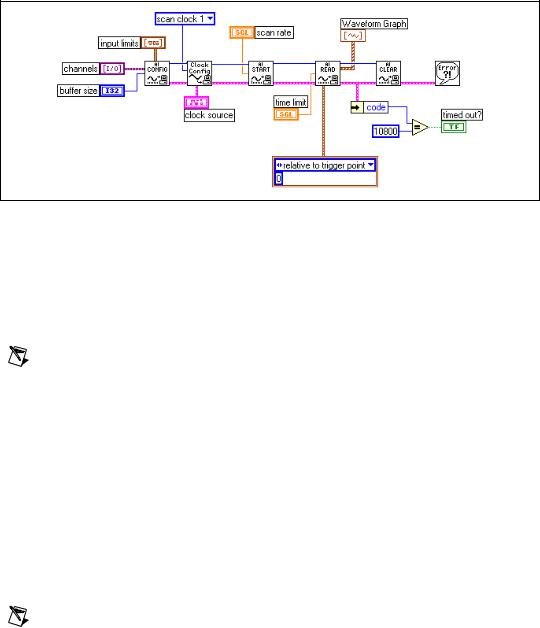
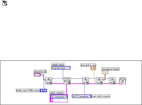
Figure 6-29 shows an example of using an external scan clock to perform a buffered acquisition.
Figure 6-29. Acquiring Data with an External Scan Clock
Externally Controlling Your Scan Clock
External scan clock control might be more useful than external channel clock control if you are sampling multiple channels, but might not be as obvious to find because it does not have the input on the I/O connector labeled ExtScanClock, the way the EXTCONV* pin does.
Note Some MIO devices have an output on the I/O connector labeled SCANCLK, which is used for external multiplexing and is not the analog input scan clock. This cannot be used as an input.
The appropriate pin to input your external scan clock can be found in
Table 6-2.
Table 6-2. External Scan Clock Input Pins
Device |
External Scan Clock Input Pin |
|
|
|
|
All E Series Devices |
Any PFI Pin |
|
(Default: PF17/STARTSCAN) |
|
|
Lab-PC+ |
OUT B1 |
1200 devices |
|
|
|
Note Some devices do not have internal scan clocks and therefore do not support external scan clocks. These devices include but are not limited to the following: PC-LPM-16,
© National Instruments Corporation |
6-43 |
LabVIEW Measurements Manual |
Chapter 6 |
Analog Input |
PC-LPM-16PnP, PC-516, DAQCard-500, DAQCard-516, DAQCard-700, NI 4060,
and Lab-LC.
After connecting your external scan clock to the correct pin,
set up the external scan clock in software. Refer to the Acquire N Scans-ExtScanClk VI in the examples\daq\anlogin\anlogin.llb for an example of how to set up the external clock in software. Two Advanced VIs, AI Clock Config and AI Control, are used in place of the Intermediate AI Start VI. This allows access to the clock source input. This is necessary because it allows access to the clock source string, which is used to identify the PFI pin to be used for the scan clock for E Series boards. The clock source also includes the clock source code (on the front panel), which is set to the I/O connector. The 0.0 wired to the Clock Config VI disables the internal clock.
Remember that the which clock input of the AI Clock Config VI should be set to scan clock (1).
Note You must divide the timebase by some number between 2 and 65,535 or you will get a bad input value error.
Because LabVIEW determines the length of time before AI Read times out based on the interchannel delay and scan clock rate, you might need to force a time limit into AI Read. In the example Acquire N Scans-ExtScanClk VI, the time limit is 5 seconds.
Externally Controlling the Scan and Channel Clocks
You can control the scan and channel clocks simultaneously. However, make sure that you follow the proper timing. Figure 6-30 demonstrates how you can set up your application to control both clocks.
Figure 6-30. Controlling the Scan and Channel Clock Simultaneously
LabVIEW Measurements Manual |
6-44 |
www.ni.com |
7
Analog Output
This chapter explains analog output for data acquisition.
Things You Should Know about Analog Output
Some measuring systems require that analog signals be generated by a DAQ device. Each of these analog signals can be a steady or slowly changing signal, or a continuously changing waveform. This section describes how to use LabVIEW to produce all of these different types of signals.
Single-Point Output
When the signal level at the output is more important than the rate at which the output value changes, you need to generate a steady DC value. You can use the single-point analog output VIs to produce this type of output. With single-point analog output, any time you want to change the value on an analog output channel, you must call one of the VIs that produces a single update (a single value change). Therefore, you can change the output value only as fast as LabVIEW calls the VIs. This technique is called software timing. You should use software timing if you do not need high-speed generation or the most accurate timing. Refer to the Single-Point Generation section, later in this chapter, for more information about single-point output.
Buffered Analog Output
Sometimes in performing analog output, the rate that your updates occur is just as important as the signal level. This is called waveform generation, or buffered analog output. For example, you might want your DAQ device to act as a function generator. You can do this by storing one cycle of sine wave data in an array and programming the DAQ device to generate the values continuously in the array one point at a time at a specified rate. This is known as single-buffered waveform generation. But what if you want to generate a continually changing waveform? For example, you might have a large file stored on disk that contains data you want to output. Because LabVIEW cannot store the entire waveform in a single buffer, you must continually load new data into the buffer during the generation. This
© National Instruments Corporation |
7-1 |
LabVIEW Measurements Manual |