

- •LabVIEW Measurements Manual
- •Worldwide Technical Support and Product Information
- •National Instruments Corporate Headquarters
- •Worldwide Offices
- •Important Information
- •Warranty
- •Copyright
- •Trademarks
- •WARNING REGARDING USE OF NATIONAL INSTRUMENTS PRODUCTS
- •Contents
- •About This Manual
- •Conventions
- •Related Documentation
- •History of Instrumentation
- •What Is Virtual Instrumentation?
- •DAQ Devices versus Special-Purpose Instruments
- •How Do Computers Talk to DAQ Devices?
- •Role of Software
- •How Do Programs Talk to Instruments?
- •Overview
- •Installing and Configuring Your Hardware
- •Measurement & Automation Explorer (Windows)
- •NI-DAQ Configuration Utility (Macintosh)
- •NI-488.2 Configuration Utility (Macintosh)
- •Configuring Your DAQ Channels
- •Assigning VISA Aliases and IVI Logical Names
- •Configuring Serial Ports on Macintosh
- •Configuring Serial Ports on UNIX
- •Example DMM Measurements
- •How to Measure DC Voltage
- •Single-Point Acquisition Example
- •Averaging a Scan Example
- •How to Measure AC Voltage
- •How to Measure Current
- •How to Measure Resistance
- •How to Measure Temperature
- •Example Oscilloscope Measurements
- •How to Measure Maximum, Minimum, and Peak-to-Peak Voltage
- •How to Measure Frequency and Period of a Repetitive Signal
- •Measuring Frequency and Period Example
- •Finding Common DAQ Examples
- •Finding the Data Acquisition VIs in LabVIEW
- •DAQ VI Organization
- •Easy VIs
- •Intermediate VIs
- •Utility VIs
- •Advanced VIs
- •Polymorphic DAQ VIs
- •VI Parameter Conventions
- •Default and Current Value Conventions
- •The Waveform Control
- •Waveform Control Components
- •Using the Waveform Control
- •Extracting Waveform Components
- •Waveform Data on the Front Panel
- •Channel, Port, and Counter Addressing
- •DAQ Channel Name Control
- •Channel Name Addressing
- •Channel Number Addressing
- •Limit Settings
- •Other DAQ VI Parameters
- •Error Handling
- •Organization of Analog Data
- •Where You Should Go Next
- •Defining Your Signal
- •Grounded Signal Sources
- •Floating Signal Sources
- •Choosing Your Measurement System
- •Considerations for Selecting Analog Input Settings
- •Channel Addressing with the AMUX-64T
- •Important Terms You Should Know
- •Single-Point Acquisition
- •Single-Channel, Single-Point Analog Input
- •Multiple-Channel, Single-Point Analog Input
- •Using Analog Input/Output Control Loops
- •Using Software-Timed Analog I/O Control Loops
- •Using Hardware-Timed Analog I/O Control Loops
- •Improving Control Loop Performance
- •Buffered Waveform Acquisition
- •Acquiring a Single Waveform
- •Acquiring Multiple Waveforms
- •Simple-Buffered Analog Input Examples
- •Simple-Buffered Analog Input with Graphing
- •Simple-Buffered Analog Input with Multiple Starts
- •Using Circular Buffers to Access Your Data during Acquisition
- •Continuously Acquiring Data from Multiple Channels
- •Controlling Your Acquisition with Triggers
- •Hardware Triggering
- •Digital Triggering
- •Analog Triggering
- •Software Triggering
- •Conditional Retrieval Examples
- •Letting an Outside Source Control Your Acquisition Rate
- •Externally Controlling Your Channel Clock
- •Externally Controlling Your Scan Clock
- •Externally Controlling the Scan and Channel Clocks
- •Single-Point Output
- •Buffered Analog Output
- •Single-Point Generation
- •Single-Immediate Updates
- •Multiple-Immediate Updates
- •Waveform Generation (Buffered Analog Output)
- •Buffered Analog Output
- •Circular-Buffered Analog Output Examples
- •Letting an Outside Source Control Your Update Rate
- •Externally Controlling Your Update Clock
- •Supplying an External Test Clock from Your DAQ Device
- •Software Triggered
- •Hardware Triggered
- •Using Lab/1200 Boards
- •Types of Digital Acquisition/Generation
- •Knowing Your Digital I/O Chip
- •653X Family
- •E Series Family
- •8255 Family
- •Using Channel Names
- •Immediate I/O Using the Easy Digital VIs
- •653X Family
- •E Series Family
- •8255 Family
- •Immediate I/O Using the Advanced Digital VIs
- •653X Family
- •E Series Family
- •8255 Family
- •Handshaking
- •Handshaking Lines
- •653X Family
- •8255 Family
- •Digital Data on Multiple Ports
- •653X Family
- •8255 Family
- •Types of Handshaking
- •Nonbuffered Handshaking
- •653X Family
- •8255 Family
- •Buffered Handshaking
- •Simple-Buffered Handshaking
- •Iterative-Buffered Handshaking
- •Circular-Buffered Handshaking
- •Pattern I/O
- •Finite Pattern I/O
- •Finite Pattern I/O without Triggering
- •Finite Pattern I/O with Triggering
- •Continuous Pattern I/O
- •What Is Signal Conditioning?
- •Amplification
- •Linearization
- •Transducer Excitation
- •Isolation
- •Filtering
- •Hardware and Software Setup for Your SCXI System
- •SCXI Operating Modes
- •Multiplexed Mode for Analog Input Modules
- •Multiplexed Mode for Analog Output Modules
- •Multiplexed Mode for Digital and Relay Modules
- •Parallel Mode for Analog Input Modules
- •Parallel Mode for the SCXI-1200 (Windows)
- •Parallel Mode for Digital Modules
- •SCXI Software Installation and Configuration
- •Special Programming Considerations for SCXI
- •SCXI Channel Addressing
- •SCXI Gains
- •SCXI Settling Time
- •Common SCXI Applications
- •Measuring Temperature with Thermocouples
- •Amplifier Offset
- •VI Examples
- •Measuring Temperature with RTDs
- •Measuring Pressure with Strain Gauges
- •Analog Output Application Example
- •Digital Input Application Example
- •Digital Output Application Example
- •Multi-Chassis Applications
- •Calibrating SCXI Modules
- •SCXI Calibration Methods for Signal Acquisition
- •One-Point Calibration
- •Two-Point Calibration
- •Calibrating SCXI Modules for Signal Generation
- •Knowing the Parts of Your Counter
- •Knowing Your Counter Chip
- •TIO-ASIC
- •Generating a Square Pulse
- •TIO-ASIC, DAQ-STC, and Am9513
- •Generating a Single Square Pulse
- •TIO-ASIC, DAQ-STC, Am9513
- •Generating a Pulse Train
- •Generating a Continuous Pulse Train
- •Generating a Finite Pulse Train
- •Counting Operations When All Your Counters Are Used
- •Knowing the Accuracy of Your Counters
- •Stopping Counter Generations
- •Measuring Pulse Width
- •Measuring a Pulse Width
- •Determining Pulse Width
- •Controlling Your Pulse Width Measurement
- •TIO-ASIC, DAQ-STC, or Am9513
- •Buffered Pulse and Period Measurement
- •Increasing Your Measurable Width Range
- •TIO-ASIC, DAQ-STC, Am9513
- •Connecting Counters to Measure Frequency and Period
- •TIO-ASIC, DAQ-STC, Am9513
- •TIO-ASIC, DAQ-STC
- •TIO-ASIC, DAQ-STC, Am9513
- •TIO-ASIC, DAQ-STC
- •TIO-ASIC, DAQ-STC, Am9513
- •Counting Signal Highs and Lows
- •Connecting Counters to Count Events and Time
- •Counting Events
- •TIO-ASIC, DAQ-STC
- •Counting Elapsed Time
- •TIO-ASIC, DAQ-STC
- •Dividing Frequencies
- •TIO-ASIC or DAQ-STC
- •The Importance of Data Analysis
- •Data Sampling
- •Sampling Signals
- •Sampling Considerations
- •Why Do You Need Anti-Aliasing Filters?
- •Why Use Decibels?
- •What Is the DC Level of a Signal?
- •What Is the RMS Level of a Signal?
- •Averaging to Improve the Measurement
- •DC Overlapped with Single Tone
- •Defining the Equivalent Number of Digits
- •DC Plus Sine Tone
- •Windowing to Improve DC Measurements
- •RMS Measurements Using Windows
- •Using Windows with Care
- •Rules for Improving DC and RMS Measurements
- •RMS Levels of Specific Tones
- •Frequency vs. Time Domain
- •Aliasing
- •FFT Fundamentals
- •Fast FFT Sizes
- •Magnitude and Phase
- •Windowing
- •Averaging to Improve the Measurement
- •Equations for Averaging
- •RMS Averaging
- •Vector Averaging
- •Peak Hold
- •Single-Channel Measurements—FFT, Power Spectrum
- •Dual-Channel Measurements—Frequency Response
- •What Is Distortion?
- •Application Areas
- •Harmonic Distortion
- •Total Harmonic Distortion
- •SINAD
- •Setting Up an Automated Test System
- •Specifying a Limit
- •Specifying a Limit Using a Formula
- •Limit Testing
- •Applications
- •Modem Manufacturing Example
- •Digital Filter Design Example
- •Pulse Mask Testing Example
- •What Is Filtering?
- •Advantages of Digital Filtering over Analog Filtering
- •Common Digital Filters
- •Ideal Filters
- •Practical (Nonideal) Filters
- •The Transition Band
- •Passband Ripple and Stopband Attenuation
- •FIR Filters
- •IIR Filters
- •Butterworth Filters
- •Chebyshev Filters
- •Chebyshev II or Inverse Chebyshev Filters
- •Elliptic (or Cauer) Filters
- •Bessel Filters
- •Choosing and Designing a Digital Filter
- •Common Test Signals
- •Multitone Generation
- •Crest Factor
- •Phase Generation
- •Swept Sine versus Multitone
- •Noise Generation
- •How Do You Use LabVIEW to Control Instruments?
- •Where Should You Go Next for Instrument Control?
- •Installing Instrument Drivers
- •Where Can I Get Instrument Drivers?
- •Where Should I Install My LabVIEW Instrument Driver?
- •Organization of Instrument Drivers
- •Kinds of Instrument Drivers
- •Inputs and Outputs Common to Instrument Driver VIs
- •Resource Name/Instrument Descriptor
- •Error In/Error Out Clusters
- •Verifying Communication with Your Instrument
- •Running the Getting Started VI Interactively
- •Verifying VISA Communication
- •What Is VISA?
- •Writing a Simple VISA Application
- •Using VISA Properties
- •Using the Property Node
- •Serial
- •GPIB
- •Using VISA Events
- •Types of Events
- •Handling GPIB SRQ Events Example
- •Advanced VISA
- •Opening a VISA Session
- •Closing a VISA Session
- •Locking
- •Shared Locking
- •String Manipulation Techniques
- •How Instruments Communicate
- •Building Strings
- •Removing Headers
- •Waveform Transfers
- •ASCII Waveforms
- •1-Byte Binary Waveforms
- •2-Byte Binary Waveforms
- •Serial Port Communication
- •How Fast Can I Transmit Data over the Serial Port?
- •Serial Hardware Overview
- •Your System
- •GPIB Communications
- •Controllers, Talkers, and Listeners
- •Hardware Specifications
- •VXI (VME eXtensions for Instrumentation)
- •VXI Hardware Components
- •VXI Configurations
- •PXI Modular Instrumentation
- •Computer-Based Instruments
- •Glossary
- •Index
- •Numbers
- •Figures
- •Figure 2-1. DAQ System Components
- •Figure 4-1. Simple Data Acquisition System
- •Figure 4-2. Wind Speed
- •Figure 4-3. Anemometer Wiring
- •Figure 4-4. Measuring Voltage and Scaling to Wind Speed
- •Figure 4-5. Measuring Wind Speed Using DAQ Named Channels
- •Figure 4-6. DAQ System for Measuring Wind Speed with Averaging
- •Figure 4-7. Wind Speed
- •Figure 4-8. Average Wind Speed Using DAQ Named Channels
- •Figure 4-9. Data Acquisition System for Vrms
- •Figure 4-10. Sinusoidal Voltage
- •Figure 4-11. Vrms Using DAQ Named Channels
- •Figure 4-12. Instrument Control System for Vrms
- •Figure 4-13. Vrms Using an Instrument
- •Figure 4-14. Data Acquisition System for Current
- •Figure 4-15. Current Loop Wiring
- •Figure 4-16. Linear Relationship between Tank Level and Current
- •Figure 4-17. Measuring Fluid Level Without DAQ Named Channels
- •Figure 4-18. Measuring Fluid Level Using DAQ Named Channels
- •Figure 4-19. Instrument Control System for Resistance
- •Figure 4-20. Measuring Resistance Using an Instrument
- •Figure 4-21. Simple Temperature System
- •Figure 4-22. Thermocouple Wiring
- •Figure 4-23. Measuring Temperature Using DAQ Named Channels
- •Figure 4-24. Data Acquisition System for Minimum, Maximum, Peak-to-Peak
- •Figure 4-25. Measuring Minimum, Maximum, and Peak-to-Peak Voltages
- •Figure 4-26. Instrument Control System for Peak-to-Peak Voltage
- •Figure 4-27. Measuring Peak-to-Peak Voltage Using an Instrument
- •Figure 4-28. Measuring Frequency and Period
- •Figure 4-29. Measuring Frequency Using an Instrument
- •Figure 4-30. Lowpass Filter
- •Figure 4-31. Measuring Frequency after Filtering
- •Figure 4-32. Front Panel IIR Filter Specifications
- •Figure 4-33. Measuring Frequency after Filtering Using an Instrument
- •Figure 5-1. Analog Input VI Palette Organization
- •Figure 5-2. Polymorphic DAQ VI Shortcut Menu
- •Figure 5-3. LabVIEW Context Help Window Conventions
- •Figure 5-4. Waveform Control
- •Figure 5-5. Using the Waveform Data Type
- •Figure 5-6. Single-Point Example
- •Figure 5-7. Using the Waveform Control with Analog Output
- •Figure 5-8. Extracting Waveform Components
- •Figure 5-9. Waveform Graph
- •Figure 5-10. Channel Controls
- •Figure 5-11. Channel String Array Controls
- •Figure 5-12. Limit Settings, Case 1
- •Figure 5-13. Limit Settings, Case 2
- •Figure 5-14. Wiring the iteration Input
- •Figure 5-15. LabVIEW Error In and Error Out Error Clusters
- •Figure 5-16. Example of a Basic 2D Array
- •Figure 5-17. 2D Array in Column Major Order
- •Figure 5-18. Extracting a Single Channel from a Column Major 2D Array
- •Figure 5-19. Analog Output Buffer 2D Array
- •Figure 6-1. Types of Analog Signals
- •Figure 6-2. Grounded Signal Sources
- •Figure 6-3. Floating Signal Sources
- •Figure 6-4. The Effects of Resolution on ADC Precision
- •Figure 6-5. The Effects of Range on ADC Precision
- •Figure 6-6. The Effects of Limit Settings on ADC Precision
- •Figure 6-7. 8-Channel Differential Measurement System
- •Figure 6-8. Common-Mode Voltage
- •Figure 6-9. 16-Channel RSE Measurement System
- •Figure 6-10. 16-Channel NRSE Measurement System
- •Figure 6-12. Using the Intermediate VIs for a Basic Non-Buffered Application
- •Figure 6-13. Acquiring and Graphing a Single Waveform
- •Figure 6-15. Using the Intermediate VIs to Acquire Multiple Waveforms
- •Figure 6-16. Simple Buffered Analog Input Example
- •Figure 6-17. Writing to a Spreadsheet File after Acquisition
- •Figure 6-18. How a Circular Buffer Works
- •Figure 6-19. Basic Circular-Buffered Analog Input Using the Intermediate VIs
- •Figure 6-20. Diagram of a Digital Trigger
- •Figure 6-21. Digital Triggering with Your DAQ Device
- •Figure 6-22. Diagram of an Analog Trigger
- •Figure 6-23. Analog Triggering with Your DAQ Device
- •Figure 6-24. Timeline of Conditional Retrieval
- •Figure 6-25. The AI Read VI Conditional Retrieval Cluster
- •Figure 6-26. Channel and Scan Intervals Using the Channel Clock
- •Figure 6-27. Round-Robin Scanning Using the Channel Clock
- •Figure 6-28. Example of a TTL Signal
- •Figure 6-29. Acquiring Data with an External Scan Clock
- •Figure 6-30. Controlling the Scan and Channel Clock Simultaneously
- •Figure 7-1. Waveform Generation Using the AO Waveform Gen VI
- •Figure 7-2. Waveform Generation Using Intermediate VIs
- •Figure 7-3. Circular Buffered Waveform Generation Using Intermediate VIs
- •Figure 8-1. Digital Ports and Lines
- •Figure 8-2. Connecting Signal Lines for Digital Input
- •Figure 8-3. Connecting Signal Lines for Digital Output
- •Figure 9-1. Common Types of Transducers/Signals and Signal Conditioning
- •Figure 9-3. SCXI System
- •Figure 9-4. Components of an SCXI System
- •Figure 9-5. SCXI Chassis
- •Figure 9-6. Measuring a Single Module with the Acquire and Average VI
- •Figure 9-7. Measuring Temperature Sensors Using the Acquire and Average VI
- •Figure 9-8. Continuously Acquiring Data Using Intermediate VIs
- •Figure 9-9. Measuring Temperature Using Information from the DAQ Channel Wizard
- •Figure 9-10. Measuring Temperature Using the Convert RTD Reading VI
- •Figure 9-11. Half-Bridge Strain Gauge
- •Figure 9-12. Measuring Pressure Using Information from the DAQ Channel Wizard
- •Figure 9-13. Inputting Digital Signals through an SCXI Chassis Using Easy Digital VIs
- •Figure 9-14. Outputting Digital Signals through an SCXI Chassis Using Easy Digital VIs
- •Figure 9-15. Ideal versus Actual Reading
- •Figure 10-1. Counter Gating Modes
- •Figure 10-2. Wiring a 7404 Chip to Invert a TTL Signal
- •Figure 10-3. Pulse Duty Cycles
- •Figure 10-4. Positive and Negative Pulse Polarity
- •Figure 10-5. Pulses Created with Positive Polarity and Toggled Output
- •Figure 10-6. Phases of a Single Negative Polarity Pulse
- •Figure 10-7. Physical Connections for Generating a Square Pulse
- •Figure 10-8. External Connections Diagram from the Front Panel of Delayed Pulse (8253) VI
- •Figure 10-9. Physical Connections for Generating a Continuous Pulse Train
- •Figure 10-10. External Connections Diagram from the Front Panel of Cont Pulse Train (8253) VI
- •Figure 10-11. Physical Connections for Generating a Finite Pulse Train
- •Figure 10-12. External Connections Diagram from the Front Panel of Finite Pulse Train (8253) VI
- •Figure 10-13. Uncertainty of One Timebase Period
- •Figure 10-14. Using the Generate Delayed Pulse and Stopping the Counting Operation
- •Figure 10-15. Stopping a Generated Pulse Train
- •Figure 10-16. Counting Input Signals to Determine Pulse Width
- •Figure 10-17. Physical Connections for Determining Pulse Width
- •Figure 10-18. Measuring Pulse Width with Intermediate VIs
- •Figure 10-19. Measuring Square Wave Frequency
- •Figure 10-20. Measuring a Square Wave Period
- •Figure 10-21. External Connections for Frequency Measurement
- •Figure 10-22. External Connections for Period Measurement
- •Figure 10-23. Frequency Measurement Example Using Intermediate VIs
- •Figure 10-24. Measuring Period Using Intermediate Counter VIs
- •Figure 10-25. External Connections for Counting Events
- •Figure 10-26. External Connections for Counting Elapsed Time
- •Figure 10-27. External Connections to Cascade Counters for Counting Events
- •Figure 10-28. External Connections to Cascade Counters for Counting Elapsed Time
- •Figure 10-29. Wiring Your Counters for Frequency Division
- •Figure 10-30. Programming a Single Divider for Frequency Division
- •Figure 11-1. Raw Data
- •Figure 11-2. Processed Data
- •Figure 11-3. Analog Signal and Corresponding Sampled Version
- •Figure 11-4. Aliasing Effects of an Improper Sampling Rate
- •Figure 11-5. Actual Signal Frequency Components
- •Figure 11-6. Signal Frequency Components and Aliases
- •Figure 11-7. Effects of Sampling at Different Rates
- •Figure 11-8. Ideal versus Practical Anti-Alias Filter
- •Figure 12-1. DC Level of a Signal
- •Figure 12-2. Instantaneous DC Measurements
- •Figure 12-3. DC Signal Overlapped with Single Tone
- •Figure 12-4. Digits vs Measurement Time for 1 VDC Signal with 0.5 Single Tone
- •Figure 12-5. Digits vs Measurement Time for DC+Tone Using Hann Window
- •Figure 12-6. Digits vs Measurement Time for DC+Tone Using LSL Window
- •Figure 12-7. Digits vs Measurement Time for RMS Measurements
- •Figure 13-1. Signal Formed by Adding Three Frequency Components
- •Figure 13-2. FFT Transforms Time-Domain Signals into the Frequency Domain
- •Figure 13-3. Periodic Waveform Created from Sampled Period
- •Figure 13-4. Dual-Channel Frequency Analysis
- •Figure 14-1. Example Nonlinear System
- •Figure 15-1. Continuous vs. Segmented Limit Specification
- •Figure 15-2. Segmented Limit Specified Using Formula
- •Figure 15-3. Result of Limit Testing with a Continuous Mask
- •Figure 15-4. Result of Limit Testing with a Segmented Mask
- •Figure 15-5. Upper and Lower Limit for V.34 Modem Transmitted Spectrum
- •Figure 15-6. Limit Test of a Lowpass Filter Frequency Response
- •Figure 15-7. Pulse Mask Testing on T1/E1 Signals
- •Figure 16-1. Ideal Frequency Response
- •Figure 16-2. Passband and Stopband
- •Figure 16-3. Nonideal Filters
- •Figure 16-4. Butterworth Filter Response
- •Figure 16-5. Chebyshev Filter Response
- •Figure 16-6. Chebyshev II Filter Response
- •Figure 16-7. Elliptic Filter Response
- •Figure 16-8. Bessel Magnitude Filter Response
- •Figure 16-9. Bessel Phase Filter Response
- •Figure 16-10. Filter Flowchart
- •Figure 17-1. Common Test Signals
- •Figure 17-2. Common Test Signals (continued)
- •Figure 17-3. Multitone Signal with Linearly Varying Phase Difference between Adjacent Tones
- •Figure 17-4. Multitone Signal with Random Phase Difference between Adjacent Tones
- •Figure 17-5. Uniform White Noise
- •Figure 17-6. Gaussian White Noise
- •Figure 19-1. Instrument Driver Model
- •Figure 19-2. HP34401A Example
- •Figure 20-1. VISA Example
- •Figure 20-2. Property Node
- •Figure 20-3. VXI Logical Address Property
- •Figure 20-4. SRQ Events Block Diagram
- •Figure 20-5. VISA Open Function
- •Figure 20-6. VISA Close VI
- •Figure 20-7. VISA Lock Async VI
- •Figure 20-8. VISA Lock Function Icon
- •Tables
- •Table 6-1. Measurement Precision for Various Device Ranges and Limit Settings (12-Bit A/D Converter)
- •Table 6-2. External Scan Clock Input Pins
- •Table 7-1. External Update Clock Input Pins
- •Table 9-1. Phenomena and Transducers
- •Table 9-2. SCXI-1100 Channel Arrays, Input Limits Arrays, and Gains
- •Table 11-1. Decibels and Power and Voltage Ratio Relationship
- •Table 13-1. Signals and Window Choices
- •Table 15-1. ADSL Signal Recommendations
- •Table 17-1. Typical Measurements and Signals
Chapter 5 Introduction to Data Acquisition in LabVIEW
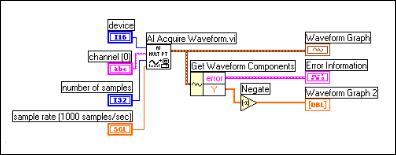
Figure 5-8. Extracting Waveform Components
Waveform Data on the Front Panel
On the front panel, use the Waveform control, available on the
Controls»I/O palette, or a Waveform Graph, available on the
Controls»Graph palette, to represent waveform data.
Use the Waveform control to manipulate the t0, dt, and Y components of the waveform or display those components as an indicator. Refer to the Waveform Control Components section for more information about each component.
When you wire a waveform to a graph, the t0 component is the initial value on the x-axis. The number of scans acquired and the dt component determine the subsequent values on the x-axis. The data elements in the Y component comprise the points on the plot of the graph.
If you want to let a user control a certain component, such as the dt component, create a front panel control and wire it to the appropriate component in the Build Waveform function.
The VI in Figure 5-9 continuously acquires 10,000 scans from a data acquisition device at a scan rate of 1,000 scans per second, which began at 7:00 p.m. You can control the ∆ t of the waveform.
LabVIEW Measurements Manual |
5-10 |
www.ni.com |