

Emerging Tools for Single-Cell Analysis
.pdfImage Sensing |
325 |
measured as an indication of the amount of light hitting the sensor. This phenomenon is harnessed in solid-state image sensor chips.
Photometry
Photometry is the technology of quantifying light intensity, and there are many ways to do this. Photon flux, for example, is one way to specify this. Photons of different wavelength, however, have different energy. Thus, if incident light energy flux is measured, the spectrum of the light affects the intensity. Commonly used image sensors, however, merely count photons, so wavelength considerations do not directly affect the measured intensity. Although different sensors have different sensitivities at different wavelengths, this can be accounted for separately. A quality image digitizer will produce a numerical array wherein each gray level is proportional to the number of photons that landed on that pixel during the exposure time.
The linearity of an image sensor specifies how accurately its output reflects the incident photon flux. Modern charge-coupled device (CCD) image sensor chips are quite linear over their entire range, and thus linearity is seldom a problem, as long as saturation (overload) of the sensor is avoided.
Video Scanning Conventions
Part of the camera design exercise is to establish the format of the output signal. This encompasses the number of scan lines, the number of pixels per line, the rate at which pixels are read out of the camera, and whether or not interlaced scanning is used.
Broadcast Scanning Conventions
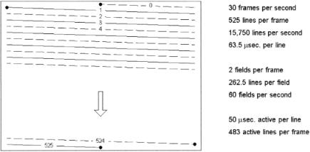
Figure 15.1 illustrates the Electronic Industries Association (EIA) RS-170 scanning convention, which is the standard for monochrome broadcast television in the United States (Fink and Christiansen, 1989; Hutson et al., 1990; Castleman, 1996). The beam scans the entire image in 525 horizontal scan lines, 30 times each second.
Each frame is made up to two interlaced fields, each consisting of 262.5 lines. The first field of each frame scans all the odd-numbered lines, while the intervening evennumbered lines comprise the second field. Interlacing yields a 60/s field rate to minimize perceived flicker, while the 30/s frame rate keeps the frequency bandwidth within the limits of broadcast television channels.
Each horizontal line scan requires 63.5 s, of which approximately 50 s (83%) contains image information (the “active” line time). Of the 525 lines per frame, 16 are lost in the vertical retrace of each field, leaving about 483 active lines per frame. The bandwidth of the standard video signal extends up to 4.5 MHz, and this allows 225 cycles, or about 550 pixels worth of information, assuming two pixels per cycle, across the active portion of each line. RS-170 video is commonly sampled at 480 lines per frame and 640 pixels per line.
The NTSC (National Television Standards Committee) timing standard for color television in the United States differs very slightly from the RS-170 convention. It
326 |
Camera Technologies for Cytometry Applications |
F i g . 15.1. The RS-170 scanning convention, used for monochrome broadcast television transmission in the United States. The CCIR convention, used in much of Europe, is similar, but it employs 625 lines per frame and operates at 25 frames per second.
was designed to accommodate color transmission while maintaining backward compatibility with existing monochrome receivers. Different scanning conventions are used in other countries. For example, the CCIR (Comité Consultatif International des Radiocommunications) standard used in much of Europe runs at 25 frames/s and uses 625 interlaced scan lines per frame. CCIR video signals are commonly sampled at 576 lines per frame and 768 pixels per line.
While there is no reason that the camera on an imaging cytometer should conform to any broadcast television standard, the realities of the marketplace dictate that the majority of mass-produced cameras and video digitizers do so. Besides, if the camera supplies a standard video signal, it facilitates watching the specimen on an ordinary TV monitor.
Other Scanning Conventions
Many cytometry applications require higher resolutions (i.e., more lines, more pixels per line) than what the RS-170 and CCIR broadcast television standards can offer. Different scanning conventions are used in the design of sensor chips intended for scientific cameras. Cameras designed specifically for scientific image sensing can be made to scan by any set of timing rules. Scientific cameras typically have larger image formats (more scan lines and pixels per line), noninterlaced scanning, and slower readout rates (to reduce the noise generated by the readout circuitry on the chip). They also may incorporate variable-length frame integration periods (to increase sensitivity) and sensor-chip cooling to reduce dark current.
Camera Performance
Although cameras differ in the approach they use to sense an image, they can be compared on the basis of their digital-image-producing performance.
Image Sensing |
327 |
Image Size. An important parameter is the size of the image a camera produces. This is specified by the maximum number of scan lines and of pixels per line. A larger image size allows more specimen area to be covered in a single image, assuming fixed resolution.
Pixel Size and Spacing. Two important characteristics are the size of the sampling aperture and the spacing between adjacent pixels. These parameters, when specified at the image plane, are fixed by the design of the image sensor chip. They scale down to the specimen plane by the magnification factor of the microscope.
Magnification. While magnification is a property of the optical system (e.g., microscope), and not of the camera, it effects a trade-off between image size and pixel spacing at the specimen. Higher magnification reduces both the pixel spacing and the area of the specimen that is covered by a single image. Lower magnification produces the opposite effect. Thus the proper magnification for a particular application will be a compromise between resolution and image area.
The magnification is usually the objective power multiplied by any auxiliary magnification that is in place. The eyepieces normally do not contribute to this calculation, but the camera adapter port may do so. The “objective power” number commonly engraved on the lens is a nominal value, and an accurate determination usually requires measurement of the pixel spacing. This can be done with the help of a suitable calibration slide.
Resolution. The word “resolution” is commonly used in three completely different ways in image cytometry. It can refer to the digital image size of a camera or digitizer, that is, the number of scan lines and pixels per line. It can address the pixel spacing at the specimen, or it can relate to the optical resolving power of the microscope, that is, the imaging instrument’s ability to reproduce small objects as separate entities. In this chapter we designate these as “digital image size,” pixel spacing,” and “optical resolution,” respectively.
Optical Resolution. According to the Raleigh criterion, one can just resolve (identify as separate) two point-source objects in a microscope image if they are separated by the distance 0.61 /NA, where NA is the numerical aperture of the objective and is the wavelength of the narrowband illumination (Castleman, 1996). This resolution is obtained only with a high-quality objective on a microscope that is in proper adjustment. To prevent loss of information, the camera should be able to reproduce detail to this degree.
The psf of a lens is the image produced by a point source in the focal (specimen) plane. To a good approximation, the half-amplitude diameter of the psf in the specimen plane is given by the Abbé distance r0 /2NA. The camera’s sampling aperture (pixel size and shape) and the microscope’s psf combine by convolution to produce the effective scanning spot. To a good approximation, its diameter is the square root of the sum of squares of the diameters of these two components. It is usually most convenient to perform these calculations in the specimen plane.

328 |
Camera Technologies for Cytometry Applications |
Linearity. The degree of linearity of the relationship between the input light intensity and the output signal amplitude is another important factor. Although the eye is not particularly critical in this department, the validity of subsequent processing can be jeopardized by a nonlinear camera.
Noise. Finally, one of the most important characteristics of a camera is its noise level. If a uniformly gray image is presented to a camera, its output will show variations in gray level, even though the input brightness is constant across the image. Such noise introduced by the camera is a source of image degradation, and it should be small relative to the contrast of the specimen.
Photon noise. “Photon noise,”or “shot noise,” results from the quantum nature of light. Even under uniform illumination conditions, the actual number of photons striking a particular pixel in any one exposure period will be random. This random variable has a Poisson distribution, in which case the variance is equal to the mean. Given the large numbers of photons involved, the Poisson distribution is approximately Gaussian. Thus shot noise can be conveniently treated as having a normal distribution with standard deviation equal to the square root of the mean.
In general, the photon noise component is equal to the square root of the number of electrons that accumulate in a well (i.e., photoelectrons plus thermal electrons):
Np |
(F QE DC)te |
(15.1) |
|
• |
|
where F is the incident photon flux, QE is the quantum efficiency, DC is the dark current, te is the exposure time, and Np is the photon noise that results from the statistical nature of light. Shot noise is usually the dominant noise source under highexposure or high-dark-current conditions.
Task Requirements. Whether or not a particular camera is adequate depends on the specific task at hand. In some applications, digitizing images with relatively few lines, pixels per line, or gray levels or with appreciable noise and nonlinearity may be sufficient. Image cytometry typically requires a high-quality camera that is capable of sensing large images with many gray levels, good linearity, and a low noise level.
TYPES OF CAMERAS
Historically, imaging tubes, such as the vidicon and its relatives, were the backbone of image cytometry. Currently, however, solid-state cameras generally offer more flexibility, better performance, and lower cost.
Tube-Type Cameras
The Vidicon. The vidicon is a common type of television image-sensing tube. It is a cylindrical glass envelope containing an electron gun at one end and a target and
Types of Cameras |
329 |
light-sensitive faceplate at the other. The tube is surrounded by a yoke containing electromagnetic focus and beam deflection coils. The faceplate is coated on the inside with a thin layer of photoconductor over a thin transparent metal film, forming the target. Adjacent to the target is a positively charged fine wire screen called the mesh. A smaller positive charge is applied to the target.
A stream of electrons is ejected from the electron gun, focused to a small spot on the target, and steered across the target in a scanning pattern by the time-varying deflection field. The moving electron beam deposits a layer of electrons on the inner surface of the photoconductor to balance the positive charge on the metal coating on the opposite side.
An optical image formed on the target causes the photoconductor to leak electrons until an identical electron image is formed on the back of the target. Electrons will thus remain in dark areas and be absent in light areas of the image.
As the electron beam scans the target, it replaces the lost electrons, causing a current flow in the target’s external circuit. This current is proportional to the number of electrons required to restore the charge and thus to the light intensity at that point. Current variations in the target circuit produce the video signal. The electron beam repeatedly scans the surface of the target, replacing the charge that bleeds away. The vidicon target is thus an integrating sensor, with the period of integration equal to the scanning frame rate.
While variations of the vidicon tube have contributed significantly to image cytometry as well as to broadcast television in the past, the present trend is toward solidstate sensors.
CCD Cameras
Silicon Light Sensors. Pure silicon can be grown in large crystals in which each atom is covalently bonded to its six neighbors in a three-dimensional rectangular lattice structure. An incident photon can break one of these bonds, freeing an electron. A thin metal layer deposited on the surface of the silicon and charged with a positive voltage creates a “potential well” that collects and holds the electrons thus freed. Each potential well corresponds to one pixel in an array of sensors. A potential well can hold about 106 electrons on typical chips.
Thermal energy also causes random bond breakage, creating “thermal electrons” that are indistinguishable from “photoelectrons.” This gives rise to “dark current,” current produced in the absence of light. The dark current is temperature sensitive, doubling for each 6°C increase in temperature. At the long integration times that are required for image sensing at low light levels, the wells can fill with thermal electrons before filling with photoelectrons. Cooling is often employed to reduce dark current and thereby extend the usable integration time.
CCD Construction. CCD chips are manufactured on a light-sensitive crystalline silicon chip, as discussed above (Janesick and Elliot, 1992). A rectangular array of photodetector sites (potential wells) is built into the silicon substrate. Photoelectrons produced in the silicon are attracted to and held in the nearest potential well. By con-
330 |
Camera Technologies for Cytometry Applications |
trolling the electrode voltages, they can be shifted as a “charge packet” from well to well until they reach an external terminal.
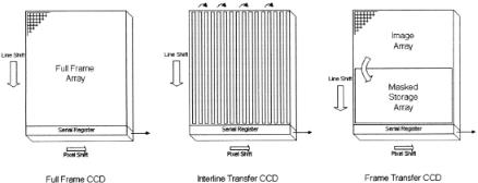
CCD Operation. There are three architectures that can be employed for reading the accumulated charge out of CCD image sensor arrays. These are (1) full-frame architecture, (2) frame transfer architecture, and (3) interline transfer architecture (Fig. 15.2).
Full-Frame CCD. Following exposure, a full-frame CCD must be shuttered to keep it in the dark during the readout process. It then shifts the charge image out of the bottom row of sensor wells, one pixel at a time. After the bottom row is empty, the charge in all rows is shifted down one row, and the bottom row is again shifted out. This process repeats until all rows have been shifted down and out. The device is then ready to integrate another image.
Frame Transfer CCD. A frame transfer CCD chip has a doubly long sensor array. The top half senses the image in the standard manner, while an opaque mask protects the storage array on the bottom from incident light. At the end of the integration period, the charge image that has accumulated in the sensing array is shifted rapidly, row by row, into the storage array. From there it is shifted out, pixel by pixel, in the standard manner, while the sensing array integrates the next image. This technique employs simultaneous integration and readout, making video-rate image sensing possible.
Interline Transfer CCD. In an interline transfer CCD every second column of sensors is covered by an opaque mask. These columns of masked wells are used only in the readout process. After exposure, the charge packet in each exposed well is shifted into the adjacent masked well. This transfer requires very little time because all charge packets are shifted at once. While the exposed wells are accumulating the next image, the charge packets in the masked columns are being shifted out in the same way as in a full-frame CCD. In an interline transfer sensor, the number of pixels per
F i g . 15.2. CCD chip operation using full-frame, interline transfer, and frame transfer architecture.
Types of Cameras |
331 |
line is half the actual number of wells per row on the chip. No more than 50% of the chip area is light sensitive, because the masked columns cover half the sensing surface. As with frame transfer, this technique employs simultaneous integration and readout.
CCD Performance. Available in a variety of configurations, CCDs give rise to compact and rugged solid-state cameras for both television and image digitizing applications. They are free of geometric distortion and exhibit highly linear response to light. CCDs are therefore emerging as the device of choice for image cytometry.
Scan Rate. The accumulated charge in a CCD chip can be scanned out at television rates (25–30 frames/s, 14 megapixels/sec) or much more slowly, if necessary, to reduce readout noise or to accommodate slower ADCs.
Dark Current. Because they can integrate for periods of seconds to hours to capture low-light-level images, CCDs are often used in fluorescence microscopy. Integration times longer than a few seconds at room temperature would fill the wells with thermal electrons before photoelectrons had a chance to build up. Thus cooling the chip to reduce dark current is a requirement for long integration times. Each 6°C decrease in temperature halves the dark current.
Because of imperfections in the crystal lattice, dark current varies significantly from one pixel to the next, particularly in less expensive chips. In long-exposure images, this leaves a “starfield” of fixed-pattern noise due to the few pixels that have the highest dark current. Because this pattern is stationary, it can be recorded and subtracted out. This effectively removes the pattern, provided the exposure is controlled so that the offending pixel wells are not allowed to saturate.
Dead Pixels. Defects in the crystal lattice can cause “dead pixels,” which cannot hold or sometimes cannot shift electrons. This can wipe out a pixel or a column of pixels. CCD sensors are graded on the number of such defects, and the higher grade chips are generally more expensive.
Readout Noise. The operation of the on-chip electronics generates noise that can contaminate the image. It ranges from a few to many electrons per pixel depending on the chip design. It gets worse as the charge is read out at a faster rate. It is usually the dominant noise factor under short-exposure, low-light conditions where the dark current and photon noise components are small.
Charge Transfer Efficiency. The charge developed at a particular pixel may be shifted as many as 2000 times, depending upon its location in the array. The charge transfer efficiency must be extremely high or significant numbers of photoelectrons will be lost in the readout process.
Fill Factor. Half or more of the available area of the sensor chip can be covered by opaque charge transfer circuitry, leaving gaps between the pixels and reducing the
332 |
Camera Technologies for Cytometry Applications |
“fill factor” below the ideal 100%. The chip can be coated with a microarray of “lenslets,” each of which focuses the incoming light it receives onto the sensitive area of one pixel well.
Blooming. Overexposure of a CCD sensor can cause excess photoelectrons to spread to adjacent pixel wells. This produces the appearance of “blooming” in the image.
Spectral Sensitivity. Silicon sensors become less sensitive at the deep blue and ultraviolet end of the wavelength spectrum. This can be overcome by a “lumigen coating” that absorbs the short-wavelength photons and then reemits the energy as longer wavelength photons that the silicon can see.
Dynamic Range. Dynamic range is computed as pixel well capacity divided by readout noise level, both measured in electrons. It is usually expressed in decibels. This parameter is independent of exposure conditions (light level and exposure time). It characterizes the performance of the chip at high light levels, where the wells become filled with photoelectrons (rather than dark current) during a relatively short exposure.
Signal-to-Noise Ratio. The signal-to-noise ratio (SNR) for an image sensor chip can be computed as the number of photoelectrons received by a well divided by the total (photon plus readout) noise level, that is,
SNR F QE te/ N p + N r |
(15.2) |
|
2 |
2 |
|
where F is the incident photon flux, QE is the quantum efficiency, te is the exposure time, Nr is the readout noise level, and Np is the photon noise that results from the statistical nature of light (see above). The SNR is quite dependent on light level and exposure time. Further, one or the other of the separate noise sources will often dominate, depending upon exposure conditions.
Charge Injection Devices
Charge injection device (CID) sensors (Williams and Carta, 1989; Kaplan, 1990) employ the same photoelectronic properties of silicon as CCDs, but they use a different method of readout.
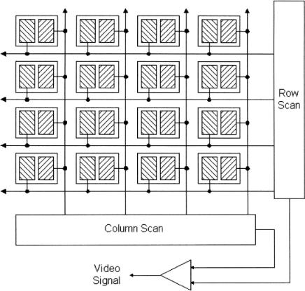
CID Construction. At each pixel site, the CID has two adjacent electrodes (Fig. 15.3) that are insulated from the silicon surface by a thin metal–oxide layer. One electrode in each pixel is connected to all the pixels in the same column, while the other electrode is connected to all the pixels in the same row. Thus, a single pixel can be addressed uniquely by its row and column address. If all rows and columns of electrodes are held at a positive voltage, the entire chip accumulates a photoelectron image.
Types of Cameras |
333 |
F i g . 15.3. CID chip operation.
CID Operation. When one electrode is driven to 0 V, the accumulated photoelectrons will shift underneath the second electrode, creating a current pulse in the external circuitry. The size of this current pulse reflects the amount of accumulated photoelectronic charge. Because the accumulated photoelectrons remain in the well after the shift, this is a nondestructive type of image readout: the pixel can be read out repeatedly by shifting the charge back and forth between the electrodes.
When both electrodes are driven to 0 V, the accumulated photoelectrons are injected into the underlying substrate, producing a current pulse in the external circuitry. The size of the pulse again reflects the amount of accumulated charge, but this process leaves the well empty. This destructive readout mode is used to prepare the chip for integrating another image.
The circuitry on the chip controls the voltages on the row and column electrodes to effect image integration and destructive and nondestructive readout. Because the CID can address individual pixels in any order, subimages of any size can be read out at any speed. Nondestructive readout allows one to watch the image accumulate
334 |
Camera Technologies for Cytometry Applications |
on the chip, which is useful when the length of the required integration period is unknown.
CID Performance. CIDs are largely immune to blooming (charge spreading to adjacent pixels) and to radiation damage. Also, with nondestructive readout, the control program can monitor the filling of the wells and selectively flush individual pixels that become full before the integration period is over.
Because CIDs do not shift charge packets across the array, charge transfer efficiency is not a concern. Unlike the CCD, a small defect in the crystal lattice affects only one pixel. Also, essentially the entire surface area is light sensitive, leaving virtually no gaps between pixels. Even with these advantages, CIDs are considerably less light sensitive than similar CCDs, and their use has not become widespread.
APS Cameras
An emerging new solid-state image-sensing technique is active pixel sensor (APS) camera technology (Janesick and Elliot, 1992; Fossum, 1993, 1995). Like CCD cameras, these are fabricated on a silicon chip, but they use complementary metal– oxide–semiconductor (CMOS) integrated circuit technology, rather than the NMOS technology more common in CCDs. CMOS allows designers to build into the sensor chip signal-processing circuitry that would normally reside elsewhere in the camera. Indeed, much of the circuitry that traditionally resides on various circuit boards in the camera can be fabricated directly on an APS image sensor chip.
An active program of APS sensor development is being pursued by the NASA Jet Propulsion Laboratory. Experimental APS camera chips have been developed with emitter–follower amplifiers at each pixel, with special noise-reducing readout circuitry and with analog-to-digital converters on the chip. Some APS chips contain circuitry that allows them to read out a specified rectangular subimage continuously and nondestructively. They can incorporate automatic exposure control and dynamic contrast control.
CMOS APS cameras offer up to a 10X reduction in camera mass and volume and a 100X reduction in power requirements, in addition to their inherently high degree of system integration. They can be fabricated by existing CMOS foundry facilities.
Existing APS chips have sensor arrays of up to 1024 1024 10- m pixels. The near future promises 2048 2048 arrays of 8- m pixels. ADC resolution, currently at 8–10 bits, will probably increase to 12 bits. Current chips require only 20 mW of power, but 5-mW chips are possible. Image readout can be done at 1 MHz now, with 10-MHz readout a future possibility. A dynamic range of 75 dB is achievable now, and 100 dB is likely to come. Noise levels of six electrons per pixel are attainable, with two electrons per pixel on the horizon. Today’s dark current level of 158 pA/cm2 will probably drop to 50 pA/cm2. Quantum efficiency is expected to increase from the present 40% to above 60%.
Single-chip cameras have been fabricated. These devices are easily interfaced into a system since they require connections only for power input and video signal output.