

27
5 Using the Computer
Now that the computer is finished you can start putting it to use. This section will describe what is required to program your new computer.
In addition to reading this section, read through the MC68HC11A1 data book, the MC6821 data sheet and the M68HC11EVB Evaluation Board user’s manual. These documents cover a lot of information not dealt with here.
Our computer was designed to be similar to the Motorola MC68HC11 Evaluation Board (EVB) which you may be familiar with. Nonetheless, our board has many differences from the EVB, so keep this in mind when you are programming. This section will cover what those differences are.
5.1Programming
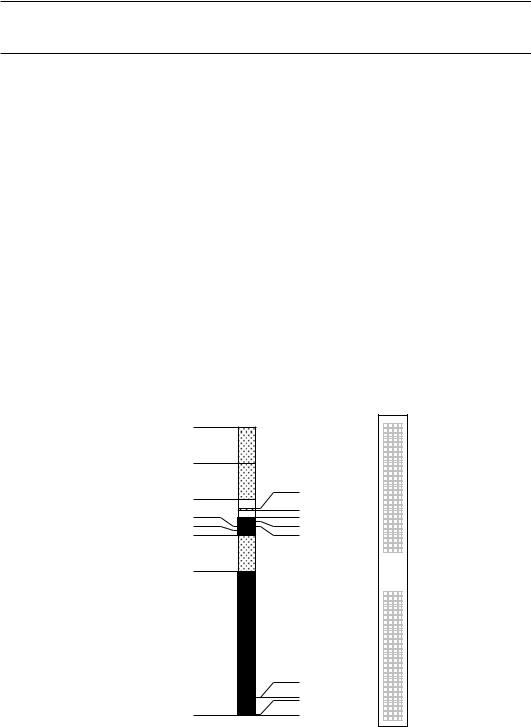
When you are programming your computer, the most important thing to be aware of is the memory map. The Chip Select PAL divides up the 64 kB memory space among the external memory and peripherals while the MC68HC11 handles the addressing of its internal devices. When there is an address space conflict between the internal and external devices, the internal devices have priority. In the memory map drawn below, you can see that the internal RAM and Control Registers overlap the 32 kB of external RAM.
|
|
PD2 |
|
|
|
PD3 |
|
|
|
PD4 |
|
Boot ROM |
|
PD5 |
|
5 |
PE0 |
||
|
|||
E000-FFFF |
|
PE1 |
|
|
PE2 |
||
|
|
||
|
|
PE3 |
|
|
|
VRL |
|
|
10 |
VRH |
|
Spare ROM |
|
PA0 |
|
|
PA1 |
||
C000-DFFF |
|
PA2 |
|
|
PA3 |
||
|
15 |
PA4 |
|
|
Internal EEPROM |
PA5 |
|
|
B600-B7FF |
PA6 |
|
|
PA7 |
||
|
|
PIA2 |
|
|
20 |
D0 |
|
PIA 2, A400-A7FF |
WR IO, AC00-AFFF |
D1 |
|
PIA 1, A000-A3FF |
RD IO, A800-ABFF |
D2 |
|
D3 |
|||
|
|
D4 |
|
|
25 |
D5 |
|
Extra ROM |
|
D6 |
|
|
D7 |
||
8000-9FFF |
|
|
|
|
|
A0 |
|
|
|
A1 |
|
|
30 |
IRQ |
|
|
|
XIRQ |
|
|
|
RESET |
|
|
|
R/*W |
|
|
|
E |
|
|
35 |
PPB0 |
|
|
|
PPB1 |
|
Main RAM |
|
PPB2 |
|
|
|
PPB3 |
|
0000-7FFF |
|
PPB4 |
|
|
40 |
PPB5 |
|
|
|
PPB6 |
|
|
|
PPB7 |
|
|
|
CB1 |
|
|
|
CB2 |
|
|
45 |
PPA0 |
|
|
|
PPA1 |
|
|
Internal Registers |
PPA2 |
|
|
PPA3 |
||
|
1000-103F |
||
|
PPA4 |
||
|
50 |
PPA5 |
|
|
Internal RAM |
PPA6 |
|
|
0000-00FF |
PPA7 |
|
|
CA1 |
||
|
|
||
|
|
CA2 |
Use this memory map to plan the organization of any hardware and software that you add to the computer.
The MC68HC11 has a large number of on-chip peripherals to take advantage of. The MC68HC11 data book describes how to program the on-chip peripherals.