

Digital design with CPLD applications and VHDL (R. Dueck, 2000)
.pdf330 C H A P T E R 8 • Introduction to Programmable Logic Architectures
Before we examine the structure of an Altera MAX7000S CPLD, we will look at the internal structure of several simpler devices that are based on similar technologies, such as the PAL16L8 and PAL16R8 low-density PLDs (largely for an historical overview), the PALCE16V8, and the GAL22V10.
These devices are based on programmable matrices of sum-of-products (SOP) circuits, as is the Altera MAX series of devices. The main programming element is the EEPROM (electrically erasable programmable read-only memory) cell. EEPROM-based devices will retain their programmed data when power is removed from the device.
The Altera FLEX series of CPLDs is based on another technology altogether. It stores logic functions in look-up tables (LUTs) that act as truth tables with four input bits. The main logic element of the FLEX series is the SRAM (static random access memory) cell. SRAM-based CPLDs must have their programming data loaded every time they are powered up. They have the advantage of being faster than EEPROM devices, with a higher bit capacity.
8.1 Programmable Sum-of-Products Arrays
K E Y T E R M S
Product line A single line on a logic diagram used to represent all inputs to an
AND gate (i.e., one product term) in a PLD sum-of-products array.
Input line A line that applies the true or complement form of an input variable to
the AND matrix of a PLD.
PAL Programmable array logic. Programmable logic with a fixed OR matrix and a programmable AND matrix.
The original programmable logic devices (PLDs) consisted of a number of AND and OR gates organized in sum-of-products (SOP) arrays in which connections were made or broken by a matrix of fuse links. An intact fuse allowed a connection to be made; a blown fuse would break a connection.
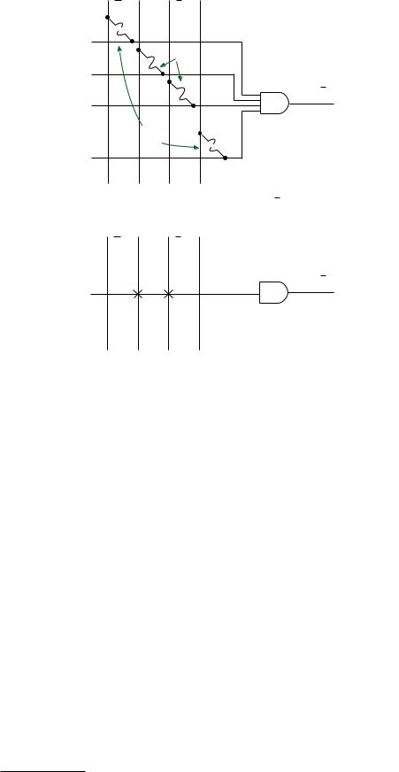
Figure 8.1a shows a simple fuse matrix connected to a 4-input AND gate. True and complement forms of two variables, A and B, can be connected to the AND gate in any combination by blowing selected fuses. In Figure 8.1a, fuses for A and B are blown. The output of the AND gate represents the product term AB, the logical product of the intact fuse lines.
Figure 8.1b shows a more compact notation for the AND-gate fuse matrix. Rather than showing each AND input individually, a single line, called the product line, goes into the AND gate, crossing the true and complement input lines. An intact connection to an input line is shown by an “X” on the junction between the input line and the product line.
A symbol convention similar to Figure 8.1b has been developed for programmable logic. Figure 8.2 shows an example.
The circuit shown in Figure 8.2 is a sum-of-products network whose Boolean expression is given by:
F A B C A B C
The product terms are accumulated by the AND gates as in Figure 8.1b. A buffer having true and complement outputs applies each input variable to the AND matrix, thus producing two input lines. Each product line can be joined to any input line by leaving the corresponding fuse intact at the junction between the input and product lines.
If a product line, such as for the third AND gate, has all its fuses intact, we do not show the fuses on that product line. Instead, this condition is indicated by an “X” through the gate. The output of the third AND gate is a logic 0, since (A A B B C C) 0. This is necessary to enable the OR gate output:
A B C A B C 0 A B C A B C

332 C H A P T E R 8 • Introduction to Programmable Logic Architectures
is done by special equipment and its associated software. The hardware and software selects each fuse individually and applies a momentary high-current pulse if the fuse is to be blown.
The main problem with fuse-programmable PLDs is that they can be programmed one time only; if there is a mistake in the design and/or programming or if the design is updated, we must program a new PLD. More recent technology has produced several types of erasable PLDs, based not on fuses but on floating-gate metal-oxide- semiconductor transistors. These transistors also form the basis of memory technolo-
gies such as electrically erasable programmable read-only memory (EEPROM or E2PROM).
8.2 PAL Fuse Matrix and Combinational Outputs
K E Y T E R M S
JEDEC Joint Electron Device Engineering Council
JEDEC file An industry-standard form of text file indicating which fuses are blown and which are intact in a programmable logic device.
Text file An ASCII-coded document stored on disk.
Checksum An error-checking code derived from the accumulated sum of the data being checked.
Cell A programmable location in a PLD, specified by the intersection of an input line and a product line.
Product line first cell number The lowest cell number on a particular product line in a PAL AND matrix where all cells are consecutively numbered.
Input line number A number assigned to a true or complement input line in a
PAL AND matrix.
Multiplexer A circuit that selects one of several signals to be directed to a single output.
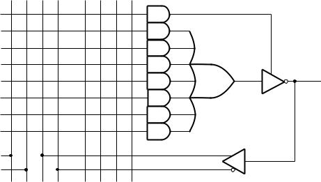
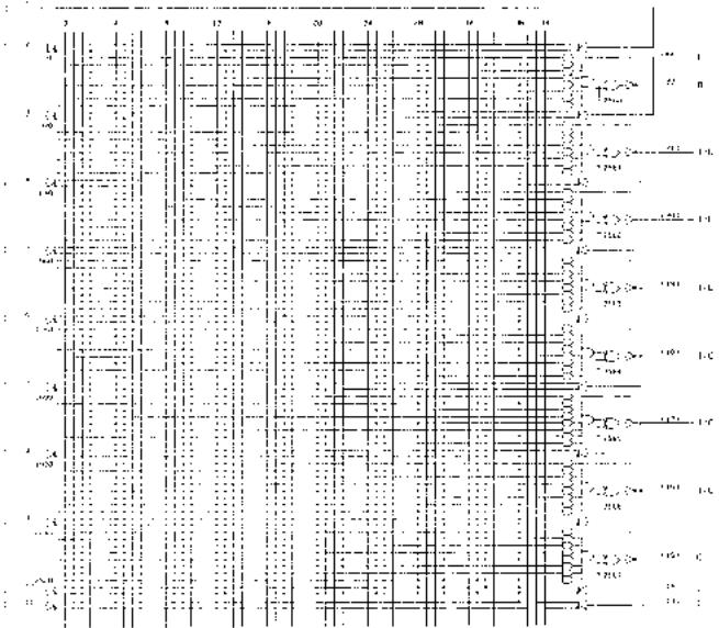
Figure 8.3 shows the logic diagram of a PAL16L8 PAL circuit. This device can produce up to eight different sum-of-products expressions, one for each group of AND and OR gates. The device has active-LOW tristate outputs, as indicated by the “L” in the part number. Each is controlled by a product line from the related AND matrix.
The pins that can be used only as inputs or outputs are marked “I” or “O,” respectively. Six of the pins can be used as inputs or outputs and are marked “I/O.” The I/O pins can also feed back a derived Boolean expression into the matrix, where it can be employed as part of another function. A detail of an I/O section is shown in Figure 8.4.
The part number of a PAL device gives the designer information about the number of inputs and outputs and their configurations, as follows:
Number of inputs
Output type:
H Active HIGH
L Active LOW
P Programmable polarity
R Registered (D flip-flop)
X XOR registered
C Complementary (both HIGH and LOW)
Number of (registered) outputs
PAL 16 R 8

8.2 • PAL Fuse Matrix and Combinational Outputs |
333 |
FIGURE 8.3
Unprogrammed PAL16L8
The numbering system has some potential ambiguities. For example, it is not possible to use 16 inputs and 8 outputs in a PAL16L8 device at the same time; 6 of the inputs are actually input/output pins. Some possible configurations are as follows:
16 inputs (10 dedicated 6 I/O) and 2 dedicated outputs
10 dedicated inputs and 8 outputs (2 dedicated 6 I/O)
12 inputs (10 dedicated 2 I/O) and 6 outputs (2 dedicated 4 I/O)
Each of the outputs of the PAL16L8 is buffered by a tristate inverter, whose ENABLE input is controlled by its own product line. When the ENABLE line of the tristate inverter is

336 C H A P T E R 8 • Introduction to Programmable Logic Architectures
FIGURE 8.6
4-to-1 Multiplexer Circuits
In order to examine the general principle of fuse programming, let us develop the programmed logic diagram for a common combinational circuit: a 4-to-1 multiplexer. (After developing the fuse maps for several examples, we will not refer to this technique again.)
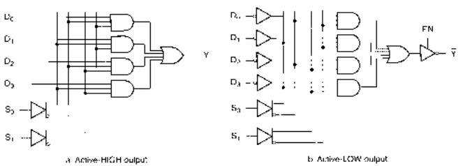
This circuit, shown in Figure 8.6a, directs one of four input logic signals, D0 to D3, to output Y, depending on the state of two select inputs S0 and S1. The circuit works on the enable/inhibit principle; each AND gate is enabled by a different combination of S1 S0. The binary state of the select inputs is the same as the decimal subscript of the selected data input. For instance, S1 S0 10 selects data input D2; the AND gate corresponding to D2 is enabled and the other three ANDs are inhibited.
The logic equation for output Y is given by:
Y D0 S1 S0 D1 S1 S0 D2 S1 S0 D3 S1 S0
Since the outputs of the PAL16L8 are active LOW, as illustrated in Figure 8.6b, we should rewrite the equation as follows:
Y D0 S1 S0 D1 S1 S0 D2 S1 S0 D3 S1 S0
The D inputs must be complemented to reverse the effect of the active-LOW output. The output is enabled when the EN input is HIGH. Figure 8.7 shows the PAL16L8A logic diagram with fuses for the multiplexer application.
8.3 PAL Outputs With Programmable Polarity
The multiplexer application developed in the previous section uses a PAL device whose output is always fixed at the active-LOW polarity. This fixed polarity is suitable for most applications, but Boolean functions that would normally have active-HIGH outputs must be implemented in DeMorgan equivalent form, which is not always very straightforward.
Some applications require both active-HIGH and active-LOW outputs. In such cases, it is useful to have a device whose output polarity is fuse programmable.
Figure 8.8 shows the logic diagram of a PAL20P8 PAL device. This device is the same as a PAL16L8, except that there are four more dedicated inputs, and the polarity of each output is programmable. The Exclusive OR gate on each output is programmed to act as either an inverter or a buffer. When its associated fuse is intact, the XOR input is grounded and passes the output of its related SOP network in true form. When combined with the output inverter, this produces an active-LOW output. When the polarity fuse is blown, the fused XOR input floats to the HIGH state, inverting the SOP output; the output pin becomes active HIGH.
8.3 • PAL Outputs With Programmable Polarity |
337 |
FIGURE 8.7
Programmed Logic Diagram for a 4-to-1 Multiplexer
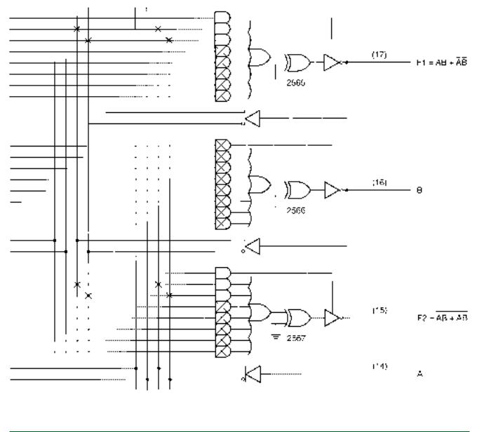
The polarity fuses are given numbers higher than those of the main fuse array. In this case, the product line fuses are numbered 0000 to 2559 and the output polarity fuses are numbered 2560 to 2567.
Figure 8.9 illustrates the selection of output polarity. Two Boolean functions, F1 and F2, are programmed into the fuse array, with outputs at pins (17) and (15), respectively. The equations are:
F1 A B A B
F2 A B A B
338 C H A P T E R 8 • Introduction to Programmable Logic Architectures
FIGURE 8.8
PAL20P8 Logic Diagram
We could, if we chose, rewrite F2 to show the output as active LOW:
F2 A B A B
The portion of the PAL20P8 logic diagram shown in Figure 8.9 represents the fuses required to program F1 and F2. Pins (14) and (16) supply inputs A and B to the matrix. The ENABLE lines of the tristate output buffers float HIGH, since all fuses are blown on the corresponding product lines, thus permanently enabling the output buffers.
The fuses numbered 2565 and 2567 select the polarity at pins (15) and (17). Fuse 2565 is blown. The fused input to the corresponding XOR gate floats HIGH, thus making the gate into an inverter. Combined with the tristate buffer, this makes pin (17) active HIGH.
Fuse 2567 is intact. This grounds the input to the corresponding XOR gate, making the gate into a noninverting buffer. Combined with the tristate output buffer, this makes pin (15) active LOW.
8.3 • PAL Outputs With Programmable Polarity |
339 |
FIGURE 8.9
PAL Outputs With Programmable Polarity
EXAMPLE 8.1 |
Show how a PAL20P8 device can be used to implement the following logic functions by |
||
|
drawing fuses on the device’s logic diagram. |
||
|
NOT: |
F1 A |
|
|
AND: |
F2 BC |
|
|
OR: |
F3 D E |
|
|
NAND: |
F4 |
FG |
|
NOR: |
F5 |
H J |
|
XOR: |
F6 |
K L K L K L |
|
XNOR: |
F7 |
M N M N M N |
How would the implementation of these logic functions differ if only active-LOW outputs were available, as in a PAL16L8?
SOLUTION The PAL20P8 has 14 dedicated inputs, 2 dedicated outputs, and 6 lines that can be used as inputs or outputs. Our functions need 13 input variables and 7 output variables. We will use six I/O pins (pins (16) through (21)) and one dedicated output (pin (15)) for the output variables.