

Chapter 7. Nano-driven Energy/Environmental
Materials
7.1 Overview
Takayoshi Sasaki
Nanoscale Materials Center, National Institute for Materials Science
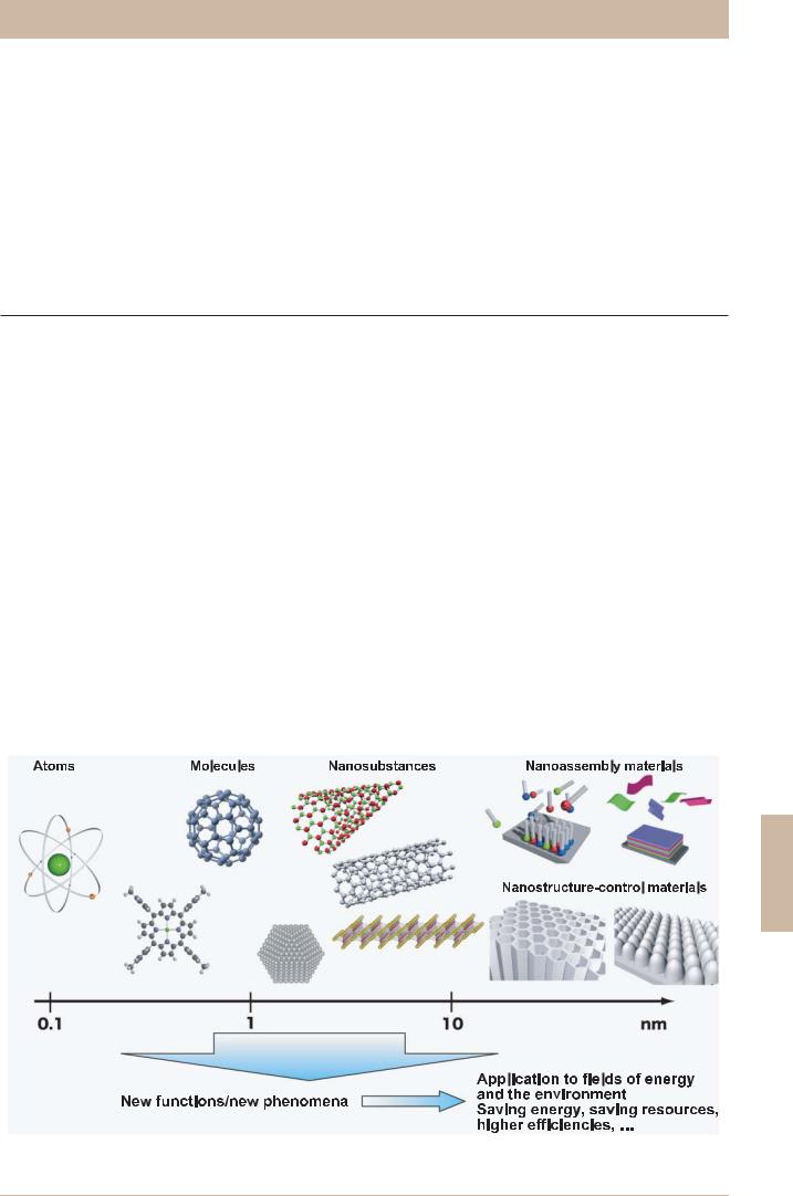
In current nanotechnology research, the search for and research into the creation of new materials and substances with a strong sense of scale, from the molecular and atomic level to sizes on the nanometer order, is being conducted and various developments are being made. Various studies are being performed with the purpose of having these new developments in materials science made through this nanotechnology serve useful roles in solving various problems in the fields of the environment and energy such as saving energy, reducing impacts on the environment and finding alternatives for scarce natural resources. In this chapter, we have organized these into four approaches (see Fig. 7.1.1).
(1)New phenomena and functions on the atomic and molecular level
(2)Development of new functions for nanoscale substances
(3)Fabrication of new materials by nanoassembly technologies
(4)Fine control of nanostructures
Regarding (1), with rapid progress in technologies that permit single electrons or molecules to be individual manipulated typified by the scanning probe microscope, it is now possible to approach phenomena and properties of materials that had been impossible up until now, and as a result, atomic switches and molecular electronics have been proposed. These proposals have the promise of permitting extremely fast operation with extremely low power consumption, among other advantages.
Regarding (2), with the discovery and synthesis of nanotubes,
nanorods, nanosheets, nanoparticles and many other new substances that have various sizes and dimensionalities, new functions deriving from the size effects and unique shapes have now been expressed. For example, high-efficiency electron emission and hydrogen storage are possible with nanotubes, while superior electronic and magnetic functions are achieved with nanosheets, so the exploration of a wide range of application is proceeding.
Regarding (3), through the development of techniques for the integration and creation of arrays of organic-inorganic nanomodules, a wide variety of materials can now be designed in the sense of “assembling them from parts” and as a result, it is now possible to develop advanced functions that would be difficult to achieve with a single substance, and the realization of high efficiency in energy conversion elements is expected.
Regarding (4), by achieving fine control of the types of atoms and their arrangement within a inorganic crystal lattice, the control of materials and substances that take advantage of nano/meso scale porous structures, and the control of the degree of dispersion of nanoparticles, clusters or the like within a medium become possible along with an extremely wide range of other technologies.
This chapter presents novel functions that have been achieved by means of the four approaches described above, along with the trends in work in recent technologies that aims to make contributions to the environment and energy sectors.
Chapter 7
Fig. 7.1.1 New developments in materials science through nanotechnology
61
Chapter 7. Nano-driven Energy/Environmental Materials
Chapter 7
7.2 Atomic Switch Materials
Tsuyoshi Hasegawa
International Center for Materials Nanoarchitechtonics, National Institute for Materials Science
1. Basics of materials
An atomic switch1) refers to a switch element that operates by utilizing an oxidation-reduction reaction to control the formation or dissipation on the atomic scale of a metallic filament formed between electrodes. In atomic switches, ion conductors are used as the main materials. Ion conductors can be divided into solid electrolytes wherein ions alone contribute to conducting electricity and electron/ion mixed conductors where electrons also contribute to conducting electricity.2)
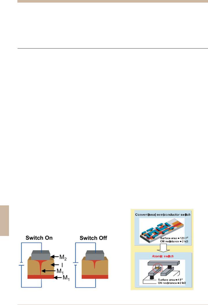
Fig. 7.2.1 presents a schematic diagram of the basic structure of an atomic switch. The switch has a M1IM2 structure comprising a metal (M1)/ion conductor (I)/metal (M2), where a metal that is soluble as ions within the ion conductor (M1) is used as one of the electrode materials.3) When a positive voltage is applied to this electrode, a metal oxidation (ionization) reaction occurs at the interface between this electrode and the ion conductor, so metal atoms (M1) become metal ions (M1+) and dissolve into the ion conductor. The metal ions (M1+) diffuse within the ion conductor toward the side of the opposite-electrode metal (M2). As a result, the metal ion concentration in the vicinity of the opposite electrode increases until it becomes supersaturated, and the metal ions that can no longer remain dissolved within the ion conductor are reduced and precipitate out as metal atoms. These precipitated metal atoms form a filament between the electrodes and the switch turns on. On the other hand, when a voltage of the opposite polarity is applied, an oxidation (ionization) reaction occurs within the precipitated metal atoms, and thus the filament is dissolved and the switch turns off.
The operating properties (operating voltage, operating speed, etc.) of the atomic switch are determined by the threshold voltages for the oxidation/reduction process, the rate of these reactions as well as the rate of diffusion of metal ions through the ion
conductor and other factors. The values of these properties depend greatly on the ion conductor materials and metal electrode materials used, as well as the combinations thereof.
2. Research trends
Development is proceeding on phase change memory, magne- to-resistance memory, resistive random access memory, atomic switches and other new devices that may serve as substitutes for semiconductor devices that have reached the extremes of miniaturization. Each of these devices is characterized by having a simple device structure and being a nonvolatile state device, so they have properties not seen in ordinary semiconductor devices.
Among these, the atomic switch achieves the switched-on state by means of a metal filament, so it is characterized in having a smaller resistance in the switched-on state than the other devices. It is suitable for the application to low power consumption and high-speed signal transmission circuits. As one example of device development taking advantage of these characteristics, let us present its application to the switching circuit of a programmable logic device.4)
When an atomic switch is used, it is possible to shrink the surface area of a switching circuit to 1/30 of that of a conventional circuit, so it is possible to incorporate many switches into a single chip (Fig. 7.2.2). As a result, it is becoming possible to develop devices that can achieve many types of functions on a single chip.
The operation of the atomic switch was initially confirmed using a sulfide system as the ion conductor, but recently its opera-
Fig. 7.2.1 Principle of operation of the atomic switch |
Fig. 7.2.2 Application to switching circuits |
62
Materials Outlook for Energy and Environment

tion has also been confirmed in a metal oxide system that can be more easily embedded into semiconductor devices.5)
3. Applications to energy and the environment
While electronic devices serve an important role in supporting today’s information-intensive society, the power consumed when they operate and the energy required to manufacture them are large, so the fact is that they place a large burden upon the environment. For this reason, the development of devices that can be manufactured at low energy costs and that can operate with low power consumption is a major problem in achieving both the sustainable expansion of the information-intensive society and an energy-saving society.
The atomic switch has a simple structure, so it can be fabricated by a manufacturing process that is roughly one-fourth as complex as that for a semiconductor device. In addition, its operating power can also be reduced to roughly a nanowatt, and thus it has a good prospect for being able to solve this problem.
4. Challenges in material science
The basic mechanism of operation of the atomic switch is the formation or dissipation of a metallic filament by means of a solid-state electrochemical reaction. However, the reaction process on the atomic level has not been fully elucidated. In order for it be used widely as a device in the future, it is necessary to be able to design and control freely its operating voltage and other device characteristics. In addition, evaluation of its durability and reliability are also essential in the course of commercialization. With atomic switches having a principle of operation that differs from that of semiconductor devices, it is not even known as to whether or not the same evaluation techniques can be used as with semiconductor devices.
Among resistive random access memory devices that have the same device structure as atomic switches, there are some wherein the transmission path (filament) is thought to be formed by oxygen loss. Elucidating a unified mechanism that includes these devices will be necessary in order to proceed with the commercialization of new devices to replace semiconductor devices. The challenges in materials science may be summarized as follows.
1)It is necessary to fully elucidate the mechanism of operation based on an elucidation of the solid-state electrochemical reactions and metal ion diffusion process on the atomic level, and also establish device design/control techniques based thereupon.
2)Accelerated lifetime test methods and other evaluation techniques must be developed with a view toward commercialization.
3)Material-dependent mappings of device characteristics must be prepared in order to handle diverse applications.
4)Research into integration processes and materials must be
conducted with the objective of early commercialization based on embedding with semiconductor devices.
References
1)K. Terabe, T. Hasegawa, T. Nakayama and M. Aono: Nature 433 (2005) 47
2)T. Kudo and K. Fueki: Solid State Ionics, Kodansha Ltd., (1990).
3)T. Sakamoto, H. Sunamura, H. Kawaura, T. Hasegawa, T. Nakayama and M. Aono: Appl. Phys. Lett. 82 (2003).
4)S. Kaeriyama, T. Sakamoto, H. Sunamura, M. Mizuno, H.
Kawaura, T. Hasegawa, K. Terabe, T. Nakayama and M. Aono: IEEE J. Solid-State Circuits 40 (2005) 168.
5)T. Sakamoto, K. Lister, N. Banno, T. Hasegawa, K. Terabe and M. Aono: Appl. Phys. Lett. 91 (2007) 092110.
Chapter 7
63
Chapter 7. Nano-driven Energy/Environmental Materials
Chapter 7
7.3 Nanoscale Materials
Minoru Osada
Nanoscale Materials Center, National Institute for Materials Science
1. Introduction
Nanosized and low-dimensional (low-D) materials, in which structure, composition and morphology are controlled on the nanoscale, exhibit unique physical and chemical properties different from those of conventional bulk materials. For this reason, the creation of novel nanomaterials are attracting substantial interest as fundamental technologies that will produce breakthroughs in various fields such as electronics, energy and environment.1,2)
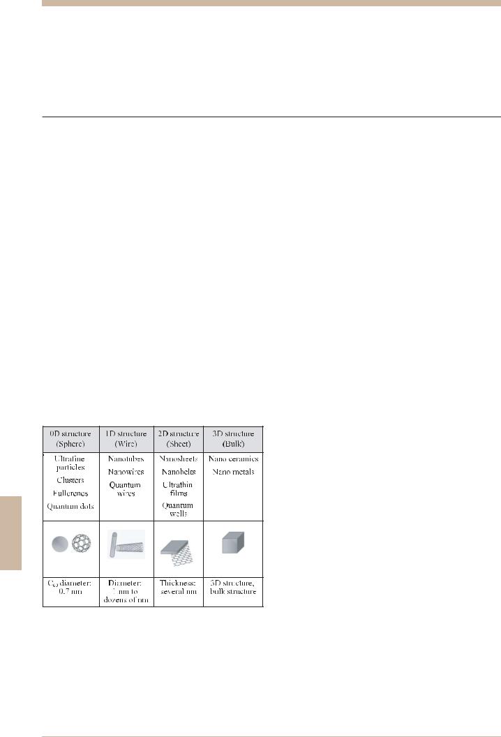
A major impetus of such nanomaterials research was the discovery of fullerenes (C60), carbon nanotubes (CNT) and other carbon nanomaterials. In inorganic cases, recent progress in synthesis techniques has lead to the successful fabrications of various nanomaterials and nanostructures such as nanoparticles, nanoclusters, nanorods, nanotubes, nanosheets (Table 7.3.1), opening up a new emerging filed for the nanotechnology in metal, semiconductor and oxide systems. Such nanomaterials are not only interesting as new functional materials, but also attracting considerable attention as key materials for creating more complex nanoarchitectures using them as fundamental building blocks.
Table 7.3.1 Structures and morphology of nanoscale materials
tional nanostructured materials by controlling material composition, organization, structure and surface boundary on nanometer order. Particularly, research of transition metal oxide nanomaterials has achieved a marked progress in recent years, and various functional nanomaterials of new forms have been reported. Those include 0D (nanoparticle, nanocluster), 1D (nanorod, nanowire) and 2D (nanosheet, nanobelt) systems in wide-gap semiconductors, ferroelectric materials, ferromagnetic materials. These oxide nanomaterials are exceptionally rich in both structural diversity and electronic properties, with potential assembly into various functional nano-devices.
Moreover, one of hot topic in nanomaterials is the successful fabrication of graphene which is an atomically thin carbon nanosheet.4) Theoretical works on the graphene has a long history, and the graphene sheet had been predicted to exhibit superior electrical, mechanical and thermal characteristics arising from its unique two-dimensional structure. However, due to the difficulty of its synthesis, the graphene had remained an unexplored frontier in carbon materials. After the successful exfoliation of the graphene sheets, research in such 2D systems has recently intensified, and there are tremendous reports on exotic properties such as 2D electron gas, high electron mobility, quantum hole effects and half metal.
2. Recent research trends
In carbon nanomaterials, recent progress in mass-production techniques has lead to their practical applications. For example, CNTs have been applied to a broad range of practical devices such as transistors, capacitors and fuel cells for mobile equipments. In inorganic nanomaterials such as metals, semiconductors and oxides, current interest concerns about the creation of func-
3.Applications in the fields of energy and environment
In recent years, research on nanomaterials has been proceeding toward application phases in various fields such as electronics, energy and environment. In these applications, a common advantage of the use of nanomaterials is the environmentally-benign aspect with low consumptions in energy and resources. These features are thought to be extremely important for a future sustainable society.
In the researches of energy and environment applications, current focus is placed on the creation of nano-ordered functional or structural materials with advanced physical properties for energy savings, which contribute to environmental improvement and conservation. In this context, there have been many reports on the creation of functional nanomaterials/nanosystems for high-energy savings and new environmenally friendly systems such as solar batteries, fuel cells, hydrogen storage nanotubes and self-cleaning TiO2 nanomaterials. In addition, the developments of self-assem- bled nanomaterials to remove hazardous chemical substances selectively, as well as the creations of new nanoporous materials which possess a selective catalytic function, are actively pur-
64
Materials Outlook for Energy and Environment
sued. In oxide nanomaterials, recent progress in nano-fabrication techniques has lead to the creation of advanced electronic materials, and various interesting properties have been explored by controlling nanostructures and nanospaces in glasses (amorphous semiconductors), cement constituents (12CaO·7Al2O3) and other commonplace materials. These materials are attracting much attention as key technologies which substitute rare metals and other scarce resources with these abundant elements.5)
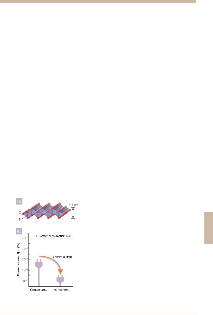
Nanomaterials are also promising as key technologies that will produce breakthroughs in advanced electronic devices.1,2) In the semiconductor technologies, increasing density requirements continue to motivate production of microelectronic devices that function reproducibly at ever smaller dimensions (a trend known as Moore’s law). However, current Si-based materials are approaching their physical limit. Continued device scaling will therefore require the replacement of new materials and/or the development of new devices structures such as single-electron devices, molecular devices. At NIMS, we are employing nanomaterial reseraches targeting for the next generation of DRAM and transistors. Recently, we have succeeded in the development of high-dielec- tric nanomaterials (titanium oxide nanosheets) that have superior energy-saving characteristics6) (Fig. 7.3.1). These nanomaterials exhibit both high dielectric constant (> 123) and low leakage current density (J< 10-7 A cm-2) for thickness down to 5 nm while eliminating problems resulting from the size effect encountered in current devices. In particular, superior energy-saving characteristics of this material is particularly important to this field, and our nanosheet thus provides new opportunities for the development of microelectronics devices that will produce low power consumption to reduce 1 µ W per device (roughly 1/100 in current devices). Moreover, this material has an additional advantage in
Fig. 7.3.1 (a) Crystal structure of titanium oxide nanosheet (Ti0.87O2), (b) Power consumption for dielectric devices of titanium oxide nanosheet and a typical high-dielectric material Ta2O5
devices fabrications, as it offers the room temperature manufacturing of active devices in the absence of costly fabrication. Such a fabrication technique is critically important to this field, and offers an environmentally friendly process that is not attainable in conventional processes.
4. Future prospects and challenges
The utilization of the superior functions of nanomaterials is expected to contribute to environmental improvement and conservation, as well as environmentally friendly technologies for new energy and energy saving. In the course of practical applications, however, conventional techniques for device fabrications cannot be applied to those new nanomaterials. In addition, nanomaterials behave differently than other similarly-sized particles. It is therefore necessary to develop specialized approaches to testing and monitoring their effects on human health and on the environment. In order to produce true breakthroughs using these nanomaterials, we have to innovate new systems incorporating nanomaterials and conduct system-oriented researches that cover diverse application fields of nanomaterials.
References
1)H. Yokoyama, Ed.: Nanomaterials Science (Japanese edition), Ohmsha, Ltd. (2004).
2)Japan Science and Technology Agency, Ed.: Nanotech and Energy (Japanese edition),, Maruzen Co., Ltd. (2007).
3)M. Osada, H. Fudozu, et al., Eds.: Special Issue “New Forms of Oxide Ceramics” (Japanese edition),, Ceramics 41 (2006) 161-305.
4)K. S. Novoselov, et al.: Science 306 (2004) 666.
5)H. Hosono, T. Kamiya: The Wondrous World of Transparent Metals (Japanese edition), Softbank Creative (2006).
6)M. Osada and T. Sasaki: Mirai-zairyo 7 (2007) 48.
Chapter 7
65
Chapter 7. Nano-driven Energy/Environmental Materials